Optical and defect properties of S-doped and Al-doped GaSe crystals∗
2017-08-30ChangBaoHuang黄昌保HaiXinWu吴海信YouBaoNi倪友保ZhenYouWang王振友andShiJingChen陈诗静
Chang-Bao Huang(黄昌保),Hai-Xin Wu(吴海信),You-Bao Ni(倪友保), Zhen-You Wang(王振友),and Shi-Jing Chen(陈诗静)
Anhui Provincial Key Laboratory of Photonic Devices and Materials,Anhui Institute of Optics and Fine Mechanics, Chinese Academy of Sciences,Hefei 230031,China
Optical and defect properties of S-doped and Al-doped GaSe crystals∗
Chang-Bao Huang(黄昌保),Hai-Xin Wu(吴海信)†,You-Bao Ni(倪友保), Zhen-You Wang(王振友),and Shi-Jing Chen(陈诗静)
Anhui Provincial Key Laboratory of Photonic Devices and Materials,Anhui Institute of Optics and Fine Mechanics, Chinese Academy of Sciences,Hefei 230031,China
S-doped and Al-doped GaSe crystals are promising materials for their applications in nonlinear frequency conversion devices.The optical and defect properties of pure,S-doped,and Al-doped GaSe crystals were studied by using photoluminescence(PL)and Fourier transform infrared spectroscopy(FT-IR).The micro-topography of(0001)face of these samples was observed by using scanning electron microscope(SEM)to investigate the influence of the doped defects on the intralayer and interlayer chemical bondings.The doped S or Al atoms form theorsubstitutional defects in the layer GaSe structure,and the positive centercould induce defect complexes.The incorporations of S and Al atoms can change the optical and mechanical properties of the GaSe crystal by influencing the chemical bonding of the layer structure.The study results may provide guidance for the crystal growth and further applications of S-doped and Al-doped GaSe crystals.
doped GaSe crystals,defect,optical properties,mechanical properties
1.Introduction
Layer GaSe crystal has been studied for decades as a nonlinear optical material.[1]It can be used to generate coherent laser in a wide spectral range from infrared[2,3]to terahertz regions[4,5]by nonlinear frequency conversions.Triggered by the discovery of the two-dimensional graphene,[6]the quasi-two-dimensional GaSe monolayers have also had their electronic,[7]optical,[8]and magnetic[9]properties investigated by experimental and theoretical methods.Moreover,it is experimentally observed that doping with different elements can modify the optical,mechanical,and electrical properties of the GaSe crystal.[10–15]
S-doped and Al-doped GaSe crystals are promising materials for applications in nonlinear frequency conversion devices.[12]It is well known that the softness of GaSe is the main flaw that limits its applications.The S-doping allows for the control of the optical properties and lattice strengthening of GaSe within wide ranges.[16]The Al-doping could maximally improve the microhardness of the GaSe crystal,but result in a degradation in its optical quality even at relatively low doping levels.[10,11]Understanding how these doped defects change the optical and mechanical properties of GaSe is important in view of its crystal growth and further applications.
The defect properties of pure GaSe and GaSe doped with elements such as In,[17]Te,[18]and Er[19]have been investigated using low temperature photo-luminescence techniques and deep-level transient spectroscopy.However,little work has been reported on defect properties of S-and Al-doped GaSe crystals.In this study,we investigate the optical and defect properties of GaSe doped with S and Al atoms.
2.Experiment
Single crystals of GaSe,S-doped GaSe(2.3 wt.%S-doping),and Al-doped GaSe(0.13 wt.%Al-doping)were grown using the Bridgman method.[20–22]A small piece of as-grown crystal was ground into powder and its x-ray powder diffraction data were recorded within the 2θ range from 10°to 90°.The samples were prepared by cleaving or cutting an ingot along the(0001)face with the typical size of 5 mm×5 mm×2 mm(Fig.1(a)).The photoluminescence(PL) measurements were carried out at 78 K by immersing the samples in liquid nitrogen.Temperature dependencies of the peak energies of PL were measured at temperatures ranging from 78 K to 240 K using a cryostat.A semiconductor laser operating at wavelength 532 nm was used as the source of excitation.The intensity of the laser beam was changed from 0.01%×60 mW/µm2to 1%×60 mW/µm2for finding the right PL intensity.The PL spectra were analyzed using a grating spectrometer and detected with a cooled S1 photomultiplier and DInGaAs2200-TE detector.Optical transparencies were measured using VERTEX70(Bruker)FT-IR spectrometer for wavelengths of 0.83–20µm:a CaF2beam splitter and an InGaAs photodiode array detector for wavelengths of 0.83–2.5µm,a KBr:Ge beam splitter and a thin-film pyro-electric detector for wavelengths of 0.25–20µm.The surface topography was observed by a Hitachi SU-8020 scanning electron microscope(SEM)instrument.
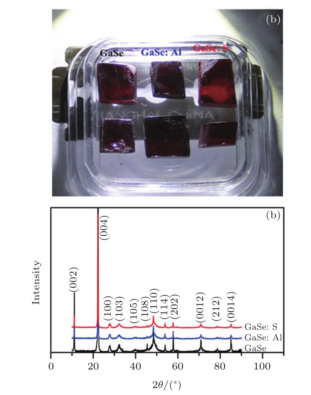
Fig.1.(color online)(a)Photograph of pure,S-doped,and Al-doped GaSe crystals(b)and their XRD patterns.
3.Results and discussion
Figure(1b)displays the x-ray diffraction(XRD)patterns measured for pure,S-doped,and Al-doped GaSe.All of these samples show similar diffraction patterns close to the standard PDF card JCPDS 97-007-1082(space group 187).The results demonstrate that S-doping and Al-doping do not change the phase structure of the GaSe crystal.
Figure 2 shows the PL spectra of pure,Al-doped,and S-doped GaSe samples at 78 K.The LA emission band is attributed to the well-known recombination of the direct free exciton.The LA peak is shifted to a high energy from pure (591 nm)to S-doped(574 nm)sample.However,the position of the LA peak(590.5 nm)of the Al-doped sample changes little compared to that of the pure sample.The LB emission band of the pure sample is attributed to the recombination of the direct exciton bound to the neutral-acceptor center.According to the previous studies,[23]the LB band is due to a Ga vacancy.For the S-doped sample,the LA band widens and may overlap with its LB band.The widening of the LA band in the S-doped sample may be induced by the non-coincidence of covalent radii and electron affinity between S atom and Se atom. For the Al-doped sample,the LB′band has the same shape as that of the pure sample.The broad LC emission band only appears in the Al-doped sample.The broad LC peak has also been observed in GaSe with excess Ga,[23]Te-doped[18]and In-doped[19]samples.The position of the LC peak is shifted to low energy compared to that of the other doped GaSe samples.The broad LC peak is attributed to the donor–acceptor pair luminescence.It is generally accepted that the major acceptor defects are gallium vacancies VGain GaSe crystals.
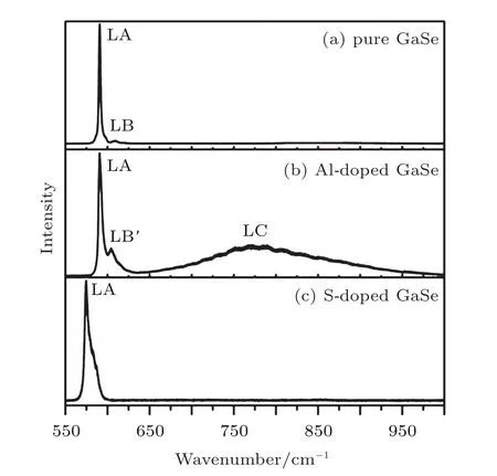
Fig.2.PL spectra of(a)pure,(b)Al-doped,and(c)S-doped GaSe crystals at 78 K.
The Al ion has+3 charge in the Al2Se3compound,while the Ga ions form(Ga–Ga)4+dimer units[11]in the GaSe structure.Therefore,the Al atom may embed in the GaSe layer structure as substitutional defectThe positive centers may induce compensation defects of VGaor Seiand form defect complexes in the GaSe crystals.GaS and GaSe have the same layer structure and valence states of elements.Doped with S,the positions of Se atoms are occupied by S atoms, and the SSedefect may be non-radiative centers.This explains why the S-doping has high levels in the GaSe structure.[24]
With the increase of temperature,the LA,LB,and LC bands are shifted to low energy,and the LB band fades away and then the LC band.At room temperature,the LB and LC bands are annihilated by lattice vibration,while the LA band is related to the short-wave cut-off wavelength.Figure 3(a) shows the PL spectra of pure,Al-doped,and S-doped GaSe samples at room temperature.The emission band of pure GaSe is observed at 2.0 eV(621 nm).The 0.13 wt.%Aldoping never really changes the emission band energy,while the 2.3 wt.%S-doping shifts the emission band energy from 2.0 eV to 2.1 eV(601 nm).This indicates that the S-doped GaSe generates a blue-shift of the short-wave cut-off wavelength compared to pure GaSe.Figure 3(b)shows the optical transparency spectra of pure,Al-doped,and S-doped GaSe samples of about 3.5 mm thickness.The 0.13 wt.%Al-doping slightly decreases the transmittance of the GaSe crystal,while the 2.3 wt.%S-doping slightly improves the transmittance in the range of 0.83–11µm.The absorption coefficient can be calculated utilizing the equation
where L is the thickness of the sample,T is the transmission, and R=(n−1)2/(n+1)2is the Fresnel reflection coefficient. The absorption coefficients of 2.3 wt.%S-doped GaSe and 0.13 wt.%Al-doped GaSe are as low as 0.1 cm−1in the range of 0.83–12µm.The Al-doping does not change the shape of the transmittance absorption spectrum of the GaSe crystal.However,the S-doped sample shows three strong multiphonon absorption peaks beyond 15µm and an obvious redshift of the long-wave cut-off wavelength.This may be caused by the substitution of SSein the layer GaSe structure.[25]
Figure 4 shows the surface topography of(0001)cleaved face observed by SEM.The cleaved face of pure GaSe sample(Fig.4(a))is imperfect and contains many step faults. The S-doped(Fig.4(c))and Al-doped(Fig.4(e))samples have smoother(0001)faces compared to pure GaSe sample.This is because the incorporation of S or Al strengthens the intralayer chemical bonding and improves the mechanical strength of GaSe multi-layer.In order to further observe the microtopography of the cleaved face,we obtain high resolution images from SEM measurements(Figs.3(b), 3(d),and 3(f)).The pure and S-doped samples contain complete and smooth(0001)faces with the size of several tens of micrometers.There is no obviously cleaved face in the micro-topography of the Al-doped sample with the size of ten micrometers:the(0001)face is rough and non-uniform compared to that of pure and S-doped samples.Moreover, unlike the pure and S-doped GaSe crystals,the Al-doped crystal is hard to cleave along the(0001)face.By using a sharp blade,several samples could be cut from an as-grown Al-doped boule.However,the cleaved surface of the sample is imperfect and contains visual step faults.We speculate that it is the interlayer interstitial defects as mentioned in PL measurement that strengthen the interlayer force of Aldoped sample and make it hard to cleave.The microhardness was measured using a Nanoindenter G200 on the cleaved (0001)face of the Al-doped GaSe crystal.The average mi-crohardness was measured at ten random points of 1 mm2area.The GaSe:Al 0.13 wt.%crystal possesses the indentation hardness of 2.27 GPa,which is 2.6 times harder than the pure GaSe crystal(0.87 GPa).[22]

Fig.3.(color online)(a)PL spectra at room temperature and(b)transparency spectra of pure,S-doped,and Al-doped GaSe crystals.

Fig.4.The SEM pictures with different resolution of(a),(b)pure,(c),(d)S-doped,and(e),(f)Al-doped GaSe crystals.
4.Conclusion
The defect and optical properties of pure,S-doped,and Al-doped GaSe crystals have been investigated using PL and FT-IR.The micro-topography of the(0001)face of these samples was observed using SEM to investigate the influences of doped defects on intralayer and interlayer chemical bondings. The Al-doped GaSe sample demonstrates a donor–acceptor pair luminescence.S-doping leads to the widening of main emission band LA and overlapping with band LB.The lowconcentration Al-doping does not change the band gap energy and the range of the transparency spectrum of the GaSe crystal.The 2.3 wt.%S-doping generates a blue-shift of the shortwave cut-off wavelength and an obvious red-shift of the longwave cut-off wavelength.
We find that the incorporation of S or Al atom modifies the optical and mechanical properties of the GaSe crystal.The doped S atom forms theisovalent substitution in the layer GaSe structure,while the doped Al atom forms non-isovalentdefect and induces defect complexes.The 2.3 wt.%S-doping can strengthen the intralayer chemical bonding,and then significantly influence the properties of electron transition and lattice vibration in the GaSe structure.The 0.13 wt.% Al-doping can strengthen the intralayer chemical bonding and interlayer force,and then significantly improve the mechanical performance of the GaSe crystal.However,the high Al-doping may produce complex defect associations and spoil the optical performance of GaSe.
[1]Allakhverdiev K R,Yetis MÖ and Ozbek S 2009 Laser Phys.19 1092
[2]Shi W,Ding Y J and Mu X 2002 Appl.Phys.Lett.80 3889
[3]Imahoko T,Takasago K and Sumiyoshi T 2007 Appl.Phys.B 87 629
[4]Zhong K,Yao J and Xu D 2010 Opt.Commun.283 3520
[5]Rao Z,Wang X and Lu Y 2011 Opt.Commun 284 5472
[6]Novoselov K S,Geim A K and Morozov S V 2004 Science 306 666
[7]Rybkovskiy D V,Arutyunyan N R and Orekhov A S 2011 Phys.Rev.B 84 085314
[8]Tang Y,Mandal K C and Mcguire J A 2016 Phys.Rev.B 94 125302
[9]Cao T,Li Z and Louie S G 2015 Phy.Rev.Lett 114 236602
[10]Zhang Y F,Wang R and Kang Z H 2011 Opt.Commun.284 1677
[11]Guo J,Xie J J and Zhang L M 2013 CrystEngComm 15 6323
[12]Guo J,Xie J J and Li D J 2015 Light Sci.Appl.4 e362
[13]Feng Z S,Guo J and Xie J J 2014 Opt.Commun.318 205
[14]Feng Z S,Kang Z H and Wu F G 2008 Opt.Express 16 9978
[15]Kang Z H,Guo J and Feng Z S 2012 Appl.Phys.B 108 545
[16]Kokh K A,Molloy J F and Naftaly M 2015 Mater.Chem.Phys.154 152
[17]Cui Y,Dupere R and Burger A 2008 J.Appl.Phys.103 013710
[18]Evtodiev I,Leontie L and Caraman M 2009 J.Appl.Phys.105 023524
[19]Hsu Y K,Chang C S and Huang W C 2004 J.Appl.Phys.96 1563
[20]Chang-Bao H,You-Bao N I and Hai-Xin W U 2015 J.Inorg.Mater 30 887
[21]Ni Y,Wu H and Huang C 2013 J.Cryst.Growth 381 10
[22]Huang C B,Ni Y B and Wu H X 2014 J.Inorg.Mater.29 557
[23]Shigetomi S and Ikari T 2003 J.Appl.Phys.94 5399
[24]Andreev Y M,Atuchin V V and Lanskii G V 2006 Mater.Sci.Eng.B 128 205
[25]Huang C B,Wu H X and Ni Y B 2016 Chin.Phys.B 25 086201
6 December 2016;revised manuscript
6 April 2017;published online 18 July 2017)
10.1088/1674-1056/26/9/094211
∗Project supported by Knowledge Innovation Program of the Chinese Academy of Sciences(Grant No.CXJJ-16M128).
†Corresponding author.E-mail:hxwu@aiofm.ac.cn
©2017 Chinese Physical Society and IOP Publishing Ltd http://iopscience.iop.org/cpb http://cpb.iphy.ac.cn
猜你喜欢
杂志排行

Chinese Physics B的其它文章
- Relationship measurement between ac-Stark shift of 40Ca+clock transition and laser polarization direction∗
- Air breakdown induced by the microwave with two mutually orthogonal and heterophase electric field components∗
- Collective motion of active particles in environmental noise∗
- Temperature dependence of heat conduction coefficient in nanotube/nanowire networks∗
- Analysis of dynamic features in intersecting pedestrian flows∗
- Heat transfer enhancement in MOSFET mounted on different FR4 substrates by thermal transient measurement∗