正交电场作用型自旋场效应管的自旋极化控制
2016-08-16肖运昌彭涛朱昌勇王日兴朱明旱
肖运昌, 彭涛, 朱昌勇, 王日兴, 朱明旱
正交电场作用型自旋场效应管的自旋极化控制
肖运昌1, 彭涛1, 朱昌勇2, 王日兴1, 朱明旱1
(1. 湖南文理学院 电气与信息工程学院, 湖南 常德, 415000; 2. 韶关学院 物理系, 广东 韶关, 512005)
研究了电场调控型自旋场效应管的量子输运过程。该场效应管主要由双正交电场和Rashba自旋轨道耦合共同调制。运用散射矩阵方法并结合介观体系的相关输运理论, 揭示了自旋场效应管在各参数调控下的自旋量子输运过程, 其自旋输运规律可由相关理论给予解释。数值计算表明, 与平行电场相比, 对于自旋轨道耦合型自旋场效应管的量子输运, 垂直电场的调制能够导致更加明显的自旋翻转。
自旋场效应管; 自旋轨道耦合; 电场
In these investigations, the external field effects, especially the electric fields, make crucial effects in the SOC realize and manipulations. Based on these works, study of the SOC system due to two orthogonal electric fields would be meaningful. Physically, study of this can not only clarify the spin properties of electric field modulations to the SFET, but also make the simulations of the SOC affected mesoscopic conductor clearly. Because that the external fields are always exist and well utilized in some semiconductor or cold atom simulated systems[22, 24-25]. In this work, by studies of the related physical properties of the SOC systems,parametric modulations to spin polarizations of the SFET are given in detail.
1 Simulated model and formulations
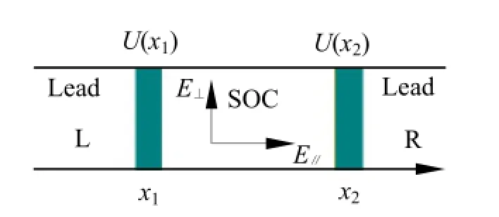
Fig.1 Schematic plots of the quantum transport in the spin field effect transistor system. The left and right are normal leads. The middle is the main effect region and subjected to two perpendicular electric fields and the Rashba spin orbit coupling.
The prototypical model of the SFET is based on a microscopic conductor, as shown in Figure 1. The model is made up by two normal leads connected with a transport semiconductor channel, in the interfaces they are affected by a couple of interfacial potentials. The electrons are confined in the y—z plane and transport along the x-axis, their variations were characterized by the transmissions and reflections of the system[10, 19-21]. Therefore, the transport of an electron in the whole transport can be simply expressed by the quasi-one-dimensional electron gas, the Hamiltonian of the electrons in Leads can be written as
where mfis the effective mass of an electron in the normal metal. The potential barriers around the interfaces are the position of x = x1and x = x2, the potentials form can be mathematical taken as
presenting the size of the central region.
Core of the model is the Rashba SOC region, which is shown in the middle part of Figure 1. As affected by two perpendicular electric fields, the Hamiltonian of the electron transport through the semiconductor can be physically treated as

From this equation the system beyond the effective-mass approximation can be found easily. Where Hvis the kinetic energy part, HSOis the Hamiltonian of the SOC part and kαis the strength of the Rashba SOC, whichcan be tuned by the wavelength of the laser beams and the atomic mass. In the semiconductor, the external field Hextincludes the parallel part E∥and the perpendicular part E⊥.
The wave function of an electron transfers from the left to the right lead can be generally expressed as

In the equation α = L, R refer to two normal leads,is the Fermi wave-vector, andare the spins in the leads withcorresponding to the parallel and antiparallel of the spin eigenstates. In the center of the model wave functions with the eigenstates can be written as
Where cnare the corresponding normalization coefficients andexpress the spinor forms as. Wave vectorscan be derived from the dispersion relation equations


According to the scattering theory of the quantum transport, the electron reflections and transmissions can be derived by the scattering matrix involving to the system[19, 27]

Thus the character of the quantum transport can be got, and more exactly the variation of the system can be measured by the number of the electrons in the propagating mode.
2 Process analysis and numerical discussions
Based on the above processions, the quantum transport in the SFET can be numerical studied, and the spin properties modulated by the external fields and SOCs also can be got. To get an intuitive physical picture of the spin quantum transport, we consider the typical InAs-based semiconductors and the mass difference is τ = ms/mf= 0.036[10, 20]. The Fermi energy is EF= 2.47 eV and the Fermi wave vector is kF= 4 nm-1, for expression convenient we defined a reference wave vector κF= 0.1 kF. Furthermore, all over the calculations the semiconductor length between two potentials is set as100 μm , the symmetric applied potentials are chosen asand controlled in the interfaces.
Firstly, the wave vector discussions are given by the analysis of the given wave formulations. Mainly consider the Eq. (5), in the spin orbit coupled region, the wave vectors are determined by the solution of this equation. For calculation convenient dimensionless units can be applied to Eq. (5), the form can be simplified as

Usually the evanescent wave should be not considered in the propagating mode, especially in the condition of the Griffith boundary conditions or the Floquet transport[28]. And the solutions of the wave vector function must be investigated comprehensively. Simply, when ignoring the perpendicular electric field effect, i.e. E⊥= 0 wave vectors can be exactly given

Direct from equation (10), we can get that the no evanescent wave will allowed in the relation of E∥<τk2. Thus in the Floquet pump transport, only the appropriatecan make the pump process realized in the semiconductor system (the unit of the parallel couplings is 0.1κF~κF)[29]. While for the stronger parallel couplings, the pump process should be calculated as the evanescent waves[28]. Moreover, by influences of the parallel couplings, the time reversal symmetry of the system is broken, and the pure spin pumped currents appear in some proper parametric settings, just as the affect of the axial magnetic field[21].
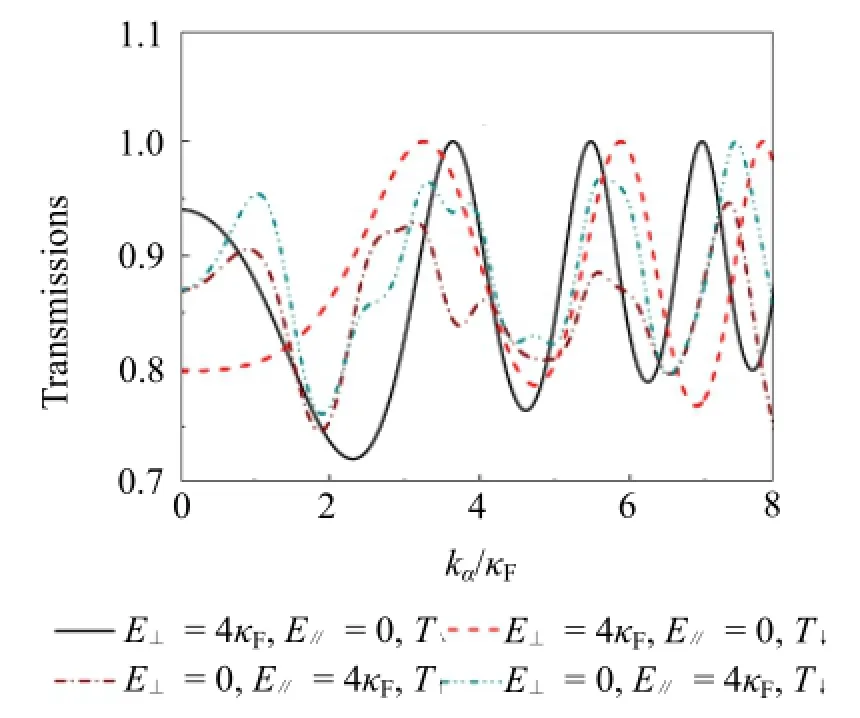
Fig.2 Total spin transmissions of the quantum transports, the solid, dashed lines correspond to different spin transmissions T↑and T↓. Here the strength of one of the parameters is set as 4kFand the other is out of considered, the spin transmissions modulated by the Rashba SOC are shown in the panels.

Furthermore, when the parallel couplings are out of consideration, the double reflection of the semiconductors is occurred. The wave vectors areand exact solutions of the quantum transport can be derived. As considering the perpendicular electric field effect, to avoid the one-band case, the strength ofwill be limited in some values. Simply, when the perpendicular couplings are much smaller than the perpendicular electric field effect//EE⊥⎕, with omitting the perpendicular couplings wave vectors can be analytical derived as When only consider the SOC affections, that just the double reflection in semiconductors, wave vectors of spin modulations can be exactly got form the quantum transport equations[20], which are reduced from corresponding ones aswhen= 0 is chosen. From the equation it also can get that a no evanescent wave transport should be set in some proper values of the perpendicular electric fields. From the analytical waves as are shown in Eq. (10) and Eq. (11), we can also get that for the radical part of the equations, the perpendicular electric field can make more significant changes to the value of the wave vectors, i.e., the small modulations ofcan lead to the imaginary wave vectors in the quantum transport.
In another way, numerical calculations of these conditions make further explanations to the analytical analysis. As all we know, when only the Rashba SOC is considered, i.e. E⊥= E∥= 0, there are no spin flipping in the spin precessions and the spin transmissions have the relations T↑↓= T↓↑= 0 and T↑↑= T↓↓, this also makes the total spin transmissions be equal T↑= T↓. Usually, Rashba SOC modulations to the quantum transport would be an excellent explanation of the physical essence of the SOC system. When one of the electric fields is exist, as shown in Figure 2, total spin transmissions of the transport are changed. For only the perpendicular electric field affect condition, as shown by the solid and dashed lines, oscillations of T↑and T↓almost keep the unchangeable amplitude but with some phase shift. This indicates that parameters of the perpendicular electric fields just make the sinusoidal differences to the final spin quantum transport, and the significant modulations to the spin transmissions are coincident with the analytical results of the previous paragraph. The dash-dot and dash-dot-dot lines show the parallel couplings effect to the spin transport,obviously, the spin transmissions oscillations to the Rashba SOC remain but the amplitude of the total spin transmissions are varied. In the oscillations the T↑and T↓almost keep the same phase and some oscillation peaks are divided from one to two. These mean that the parallel couplings will make significant influences to the amplitude and the phase of the simulated SOC transport. Particularly, the spin transmission resonant can easily occur in some Rashba SOC modulations, though as the system is affected by the barrier potentials and the perpendicular electric fields.
Polarizations of the one electric field effect to the transport are also shown in Figure 3. Form the figure it can get that in both of the two conditions, the parameters make the polarization oscillations versus the Rashba SOC vary with each other. Non periodical oscillations are appeared, and the value of the polarizations can make the positive and negative change with the SOC regulation. For the same strength modulation, the amplitude of the E⊥affected oscillation is larger than that of the E∥affected one, as shown by the solid and dashed lines of Figure 3. This phenomenon tells that compared to the parallel coupling, the perpendicular electric field makes a more remarkable spin flipping to the quantum transport of the simulated system.

Fig.3 Spin polarizations of the quantum transports. Only one of the parameters is set and the other one is out of considered. The solid lines correspond to E⊥= 4κFand the dashed lines correspond to E∥= 4κF.
Then the electric field modulations to the transmission properties of the SOC system can also be calculated, numerical discussions are given as follows. In this condition, we consider there certain one of the two perpendicular electric fields and the SOC strength are set and investigate the transmission oscillations by modulated the other parameter. Though as subjected to the fixed size and SOC strength of the system, the transmissions are still oscillated with the electric fields, as shown in Figure 4. For fixed parameters, the transmissions are oscillated with the small parallel coupling around the large values. While strengthen the parallel coupling, the amplitude of the spin down transmission oscillations becomes larger, and the spin up transmission oscillations almost keep in a same value, these can be seen in Figure 4(a).
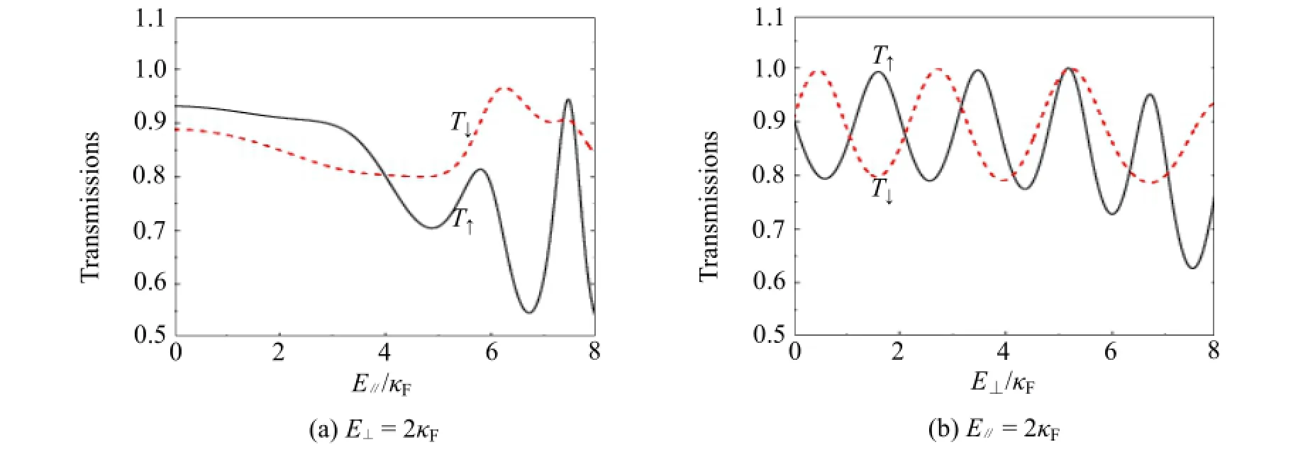
Fig.4 Total spin transmissions of the quantum transports, the solid, dashed lines correspond to different spin transmissions T↑and T↓. Here the strength of Rashba SOC and one of the electric fields are set as 5κFand 2κFseparately. The spin transmissions are modulated by the other electric field as shown in the panels.
This comes from the parallel coupling makes weaker modulations than the perpendicular electric field asthe results of showing before. When consider the perpendicular electric field modulations to the system, the transmissions oscillations are shown in Figure 4(b). From the panel it can get that though the small perpendicular electric field can make obviously transmissions oscillations. In these oscillations, the spin down and spin up transmissions keep the same amplitude, and a half period phase difference appears in the small value. As increasing the strength of E⊥, the phase differences are changed, and in some values the perpendicular electric field can make the spin down and spin up transmissions achieve the peaks in the same phases, as shown in the Figure 4(b). Also the large enough E⊥can make the transmissions oscillate in larger amplitudes. This comes from the strong spin flipping characteristic of the perpendicular electric field.
Finally, numerical discussions of the polarization properties due to the electric field effects in the quantum transport of the SOC system are given. Referring these calculations spin polarizations modulated by the accompanied parameters can be got as Figure 5. From the figure it can find that as consider the effects of one of the fixed electric fields, polarization oscillations versus the other electric field are still exist and the amplitudes are increased. Furthermore, in these conditions, even though taking into the small strength of the perpendicular electric field, the spin transmissions are all of large polarizations. For the large electric field modulation, the polarizations all keep the same oscillations style but strengthen in amplitudes as shown in Figure 3, which come from the significant modulation of the electric field modulations. So it is very important to choose proper electric field settings in the SOC system.

Fig. 5 Spin polarizations of the quantum transports. One of the electric fields is set as 2κFand the Rashba SOC is set as 5κF. The other electric field (Ed, solid lines correspond to the E∥modulation and the dashed lines correspond to the E⊥modulation) modulations to the spin polarizations.
3 Conclusion
Particular for the quantum transport of the SOC system, we have studied the spin transmission and spin polarization properties by the SOC and two perpendicular electric field modulations. Comparing with different parametric modulations of the quantum transport, we clearly obtained the SOC and the electric field effects to the quantum transport of the SOC system. Furthermore, including the SOC and size oscillations effect of the system, the electric fields also make the spin transmissions and spin polarizations oscillate thoroughly. Furthermore, the parallel coupling modulations lead to the spin flipping of the quantum transport in the SOC system, and the perpendicular electric field can make an even more remarkable spin flipping to the spin transport. These can be easily understood by the analytical results of the spin wave vectors in some specific parametric modulations. Numerical results indicate that some complicate parametric modulations are still almost kept same modulations of the spin precessions.
Acknowledgments: Thanks Doctor Zhong Q H and Luo W for their helpful and interesting discussions.
[1] Datta S, Das B. Electronic analog of the electro-optic modulator [J]. Appl Phys Lett, 1990, 56(7): 665-667.
[2] Ohno Y, Young D K, Beschoten B, et al. Electrical spin injection in a ferromagnetic semiconductor heterostructure [J]. Nature, 1999, 402: 790-792.
[3] Schapers Th, Nitta J, Heersche H B, et al. Interference ferromagnet/semiconductor/ferromagnetic spin field effect transistor [J]. Phys Rev B, 2001, 64: 125314(1-5).
[4] Khodas M, Shekhter A, Finkelstein A M. Spin polarization of electrons by nonmagnetic heterostructures: The basics ofspin optics [J]. Phys Rev Lett, 2004, 92(8): 086602(1-4).
[5] Bercioux D, De Martino A. Spin-resolved scattering through spin-orbit nanostructures in graphene [J]. Phys Rev B, 2010,81: 165410(1-9).
[6] Saarikoski H, Vazquez-Lozano J E, Baltanas J P, et al. Topological transitions in spin interferometers [J]. Phys Rev B,2015, 91: 241406(R)(1-5).
[7] Wolf S A, Awshalom D D, Buhrman R A, et al. Spintronics: A spin-based electronics vision for the future [J]. Science,2001, 294:1 488-1 495.
[8] Zutic I, Fabian J, Das Sarma S. Spintronics: fundamentals and applications [J]. Rev Mod Phys, 2004, 76: 323-410.
[9] Rashba E I. Theory of electrical spin injection: Tunnel contacts as a solution of the conductivity mismatch problem [J]. Phys Rev B, 2000, 62(24): 67-70.
[10] Lee M, Choi M S. Ballistic spin currents in mesoscopic metal/In(Ga)As/metal junctions [J]. Phys Rev B, 2005, 71:153306.
[11] Zhu Z G, Jia C L, Berakdar J. Proposal for fast optical control of spin dynamics in a quantum wire [J]. Phys Rev B, 2010,82: 235304(1-5).
[12] Zhang Y, Shibata K, Nagai N, et al. Terahertz intersublevel transitions in single self-assembled inas quantum dots with variable electron numbers [J]. Nano Lett, 2015, 15(2): 1 166-1 170.
[13] Mireles F, Kirczenow G. Ballistic spin-polarized transport and Rashba spin precession in semiconductor nanowires [J]. Phys Rev B, 2001, 64: 024426(1-13).
[14] Kirczenow G. Ideal spin filters: A theoretical study of electron transmission through ordered and disordered interfaces between ferromagnetic metals and semiconductors [J]. Phys Rev B, 2001, 63: 054422(1-6).
[15] Schliemann J, Egues J C, Loss D. Nonballistic spin-field-effect transistor [J]. Phys Rev Lett, 2003, 90: 146801(1-4).
[16] Hasan M Z, Kane C L. Colloquium: Topological insulators [J]. Rev Mod Phys, 2010, 82: 3 045-3 047.
[17] Qi X L, Zhang S C. Topological insulators and superconductors [J]. Rev Mod Phys, 2011, 83: 1 057-1 110.
[18] Sugahara S, Takamura Y, Shuto Y, et al. Field-effect spin-transistors [M]. Springer Netherlands, 2016: 1 243-1 279.
[19] Ramaglia V M, Bercioux D, Cataudella V, et al. Spin polarization of electrons with Rashba double-refraction [J]. J Phys Cond Matt, 2004, 16: 9 143-9 1554.
[20] Xiao Y C, Zhu R, Deng W J. Ballistic transport in extended Datta-Das spin field effect transistors [J]. Solid State Commun,2011, 151: 1 214-1 219.
[21] Xiao Y C, Wang R X, Deng W Y. Quantum transport of the semiconductor pump: Due to an axial external field [J]. Physica B, 2014, 449: 42-46.
[22] Brantut J P, Meineke J, Stadler D, et al. Conduction of ultracold fermions through a mesoscopic channel [J]. Science, 2012,337(6098): 1 069-1 071.
[23] Stadler D, Krinner S, Meineke J, et al. Observing the drop of resistance in the flow of a superfluid Fermi gas [J]. Nature,2012, 491(7426): 736-739.
[24] Zhang J Y, Ji S C, Chen Z, et al. Collective dipole oscillations of a spin-orbit coupled Bose-Einstein condensate [J]. Phys. Rev Lett, 2012, 109: 115301(1-4).
[25] Lin Y J, Jimenez G, Spielman I B. Spin-orbit-coupled Bose-Einstein condensates [J]. Nature, 2011, 471: 83-85.
[26] Molnar B, Peeters F M, Vasilopoulos P. Spin-dependent magnetotransport through a ring due to spin-orbit interaction [J]. Phys Rev B, 2004, 69: 155335(1-11).
[27] Jiang K M, Yang J, Zhang R, et al. Ballistic transport properties in spin field-effect transistors [J]. J Appl Phys, 2008, 104:053722(1-11).
[28] Moskalets M, Büttiker M. Floquet scattering theory of quantum pumps [J]. Phys Rev B, 2002, 66: 205320(1-10).
[29] Cahay M, Bandyopadhyay S. Conductance modulation of spin interferom [J]. Phys Rev B, 2003, 68: 115316(1-5).
(责任编校: 刘刚毅)
Spin polarization control of the spin field effect transistors due to two orthogonal electric fields
Xiao Yunchang1, Peng Tao1, Zhu Changyong2, Wang Rixing1, Zhu Minghan1
(1. College of Electrical and Information Engineering, Hunan University of Arts and Science, Changde 415000,China; 2. Department of Physics, Shaoguan University, Shaoguan 512005, China)
Quantum transports of the spin field effect transistors (SFET) tuned by electric field are investigated in this work. Target modulations of the SFET are two orthogonal electric fields and the Rashba spin-orbit coupling (SOC). By using the scattering matrix method and related transport theories in mesoscopic systems, investigations reveal that spin quantum transport of the SFET can be adjusted by the parametric modulations. Implements of the spin transport are systematic presented in theory. Numerical calculations show that compared to the parallel electric field, the perpendicular coupling modulations can make an even more remarkable spin flipping to the quantum transport in the SOC system.
spin field effect transistors; spin orbit coupling; electric fields
O 471
1672-6146(2016)03-0038-07
10.3969/j.issn.1672-6146.2016.03.009
肖运昌, phyxiaofan@163.com。
2016-04-18
湖南文理学院博士启动基金(10133004); 湖南省自然科学基金(12JJ3061); 湖南省自然科学基金(2016JJ3096)。processions, not only the reliable spin injection measurements, but also the detailed spin precessions in the materials are detailed figured, results demonstrate that they are all adaptable to describe and understand spin properties of electrons in the devices. Lately, cold atom analog of the mesoscopic conductor has been realized with6Li atoms by Brantut et al[22]. As a foundation research, they show that the electric resistance is detectable even in the defect-free device. The typical quantum phenomena of physics such as quantized conduction, local resistance, and quantum phase transitions have been observed accordingly[23]. This work makes the quantum transport in cold atom simulations come true. In another recent experimental study, the spin orbit coupled system simulated by the cold atoms is successfully realized and investigated by Zhang et al[24]. In the broad parameter region, dynamics of the center-of-mass dipole oscillation can be studied, where spin-orbit coupling (SOC) is one of the main simulated parameters with the sum-rule approach. There are observable quantum phase transitions, which separate the magnetic nonzero-momentum condensate from the nonmagnetic zero-momentum phase, make the analogy of the spin orbit coupled bosons be achieved. All these results are in good agreements between the experimental and theoretical investigations.
With rapid developments in investigations of the spin electrons[1-6], lots of related electronic devices named spintronics[7-8], physical phenomenon such as spin transports[9-12], spin precessions[13], injections and detection of spin polarizations[14], have been followed and thoroughly studied in recent years. One based on these fundamental researches and ingenious applications is realization of the spin field effect transistors (SFET), which has sparked various investigations in physical processes of quantum properties and spin precessions[15-17]. Generally speaking, the key advantage of the SFET is opening up a new possibility of the spin electrons control, which becomes a fantastic and vigorous reference for basic experimental tests in solid state systems[7, 18].
At the beginning of the investigations of SFET, feasibilities of theory and experiments in semiconductors with delta potentials on the chip have been studied in detail[19-21]. For their easy modulations to the spin