Research on the Preparation and Chromaticity Coordinates Shift Mechanism of Organic White Light Top-Emitting Devices
2016-07-12WANGGuanghuaZHAOHuiqiongDENGRongbinDUANYuSUNHaoZHANGXiaodanZHOUQinQIANJinmeiWANRuiminJIHuaxiaJIRongbin
WANG Guang-hua,ZHAO Hui-qiong,DENG Rong-bin,DUAN Yu,SUN Hao,ZHANG Xiao-dan,ZHOU Qin,QIAN Jin-mei,WAN Rui-min,JI Hua-xia,JI Rong-bin
1. Yunnan Olightek Opto-Electronic Technology Co., Ltd., Kunming 650223, China 2. Kunming Institute of Physics, Kunming 650223, China
Research on the Preparation and Chromaticity Coordinates Shift Mechanism of Organic White Light Top-Emitting Devices
WANG Guang-hua1,2,ZHAO Hui-qiong1,2,DENG Rong-bin1,DUAN Yu1,2,SUN Hao1,ZHANG Xiao-dan1,2,ZHOU Qin1,QIAN Jin-mei1,WAN Rui-min1,2,JI Hua-xia1,JI Rong-bin2
1. Yunnan Olightek Opto-Electronic Technology Co., Ltd., Kunming 650223, China 2. Kunming Institute of Physics, Kunming 650223, China
The top emission organic light-emitting devices were fabricated on the multi-layers metal anode with co-doping method in single host system. In experiment, the multilayer Al/Mo/MoO3anode on silicon are deposited, systematically analyzed the effect MoO3thickness on the reflectance and found the mechanism of the MoO3thickness variation to the reflectivity of Al/Mo/MoO3on silicon. Experimental results showed that the luminous intensity of blue, green and red appear to change according to the current density increase, and compared with the red intensity, the luminous intensity of blue and green gradually increased. The emission in this host-guest co-doping system is considered to usually involve two emission mechanisms, energy transfer and carrier trapping, and the energy transfer and carrier trapping between the host-guest should be responsible for chromaticity coordinates shift of organic white emitting light devices. In addition, through further study, it is proved the electroluminescence intensity of dopant linearly decrease with the driving voltage applied to the device by theoretical and experimental results.
White organic light-emitting diode; Color-shift; Energy transfer; Carrier trapping
Introduction
Organic light-emitting diodes (OLEDs) have attracted much attention because of their particular advantages with high resolution, fast response, self-luminous, high image quality, compact size, very low power, and can be prepared on flexible substrate, to be recognized as the most ideal and the most promising next generation display technology[1-2]. White light emission is usually obtained by doping an active host material with several dyes or by using a multilayer structure with two or more emitting layers, in this case, different dopants can conceivably compete with one another under different driving conditions due to differences in the exciton energy and shifts in the recombination zone. Consequently, the color performance will vary with different driving conditions, which inevitably presents additional difficulties for lighting applications and down-conversion displays with backlight units of WOLED and color filters. For these applications, CIE coordinates variation during operation will distort the color of the illuminated object and will suffer from distortions of the pixel emitting color and non-uniform color distribution over the panel under the same driving conditions. Unfortunately, many WOLEDs, except a few with an optimized device structure design, show the variation in color with the bias voltage or current, regardless of their structures as a single layer or multilayer. Therefore, in order to demand for different lighting and displays applications, WOLED must be developed with high efficiency and long operation life, besides with high color stability. In this work, we report on efficient WOLEDs that possess one luminous layer with co-evaporation methods, and briefly discussed the chromaticity coordinates shift mechanism of white organic light emitting devices and to shed light on the rational structure design of high quality WOLEDs with small or no color shifts.
1 Experiments
The organic light-emitting devices are prepared on the 1 600-nm-SiO2-coated silicon substrate. Prior to the deposition, the silicon substrate was ultrasonically washed with acetone, alcohol, deionized water successively. After blowing with N2gas, the silicon substrate are placed into plasma cleaning machine to further wash, then deposited multi-layers metal anode with thermal evaporation system on substrate. Then the substrate was transferred into a vacuum chamber for film deposition, the devices were fabricated by the thermal evaporation of the organic materials on the multi-layers metal anode. The organic layers and electrode were deposited by vacuum vapor deposition at <2×10⁻⁴Pa, and the thicknesses of these deposited layers and the evaporation rate of individual material were monitored in vacuum with quartz crystal monitors. The typical device structure was metal anode (60 nm)/HIL(15 nm)/HTL(10 nm)/EML(20 nm)//ETL(15 nm)/EIL(10 nm)LiF(1 nm)/Mg∶Ag(10 nm)/ITO(35 nm), where ITO is used the out-coupling layers and encapsulation layers of top-emission organic light-emitting devices. The active area of the devices was controlled at 20 mm2. The electroluminescence spectra were measured using a PR655 spectrophotometer. The luminance-current versus voltage characteristics were measured simultaneously with a Keithley 2400 voltage-current source. All measurements were carried out at room temperature under ambient conditions.
2 Results and discussion
2.1 Preparation of white organic light emitting devices
Recently, the use of MoO3as an anode buffer layer in OLEDs offers advantages such as less contamination, easy thermal deposition and energy level matching with organic molecules[3]. It has been experimentally proven that the use of MoO3and MoO3doped hole-transporting material as anode modification layers significantly reduces the operational voltage and improves the efficiency and lifetime of OLEDs. First of all, two layer structure anode was prepared on silicon substrate with high reflectivity metal Al and the electrochemical stability metal Mo, the surface of metal anode were treated by the hybrid plasma of oxygen and nitrogen with different time, the experimental results showed that according to the increasing of treating time, the metal Mo of anode gradually turned into a metal oxide at the surface, and the metal oxide layer produced additional series resistance, which lead to the driving voltage increase. At the same time, the thickness variations of oxide layer lead a change in the optical properties of the surface of the anode, such as reflectance and transmittance. In order to evaluate the effect of anode surface oxide layer change on the optical properties, in experiment, based on the transfer matrix theory and optical constants of metal and oxide molybdenum in Fig.1, the reflection of multilayer anode were numerically calculated with matlab program. From the experimental results in Fig.2, it can be seen that the reflectance of anode gradually increase with the thickness increase of MoO3layer, the reason why is that the refractive index (n) of molybdenum is higher than oxide molybdenum, but the extinction coefficient (k) of molybdenum is smaller than oxide molybdenum. Since the extinction coefficient of materials is proportional to absorption coefficient, the relation can be written as
(1)
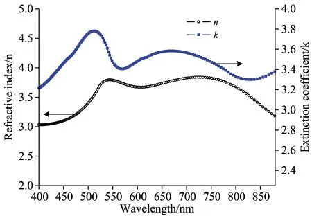
Fig.1 Optical constants of molybdenum and oxide molybdenum
the higher the extinction coefficient (k) of materials, the stronger the absorption coefficient (α), therefore, the reflectivity of multilayer anode (silicon/Al/Mo/MoO3) films increases as the MoO3thickness increases, but the MoO3thin films layers should be sufficiently thin that it contribute negligibly to the OLED series resistance. In this experiment, the MoO3thickness is preferably controlled at 1 nm.
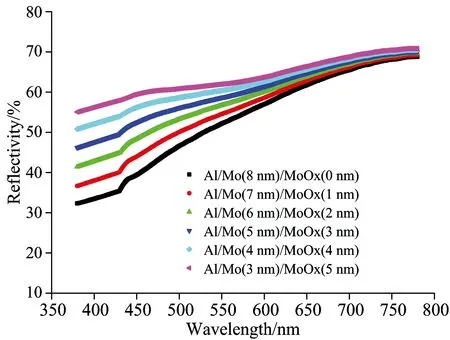
Fig.2 The reflectivity of multilayer anode with different MoO3 thickness
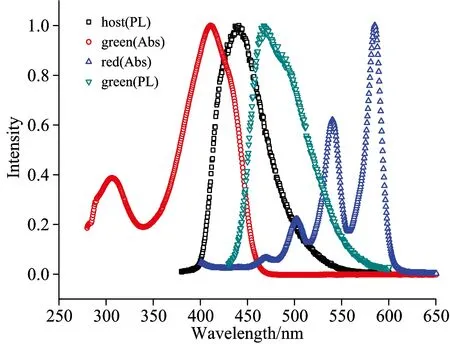
Fig.3 The absorption and photoluminescence spectra of host or guest
There are many approaches to realize white emission[4], e.g.,WOLEDs structures with blue/yellow (or red) emitters or red/green/blue ones, a single emission material with broad emission wavelength range or several side chains as emission moieties, blue OLEDs together with a yellow down-conversion layer, stacked WOLEDs, micro-cavity-based WOLEDs, etc. In this paper, we doped a red and green guest into a blue host as emissive layer by co-deposition to prepare WOLEDs. Fig.3 shows the absorption and photoluminescence spectra of host or guest in emissive layer. There is complex energy transfer mechanism in co-doping system of the emissive layer, the energy of host materials can be transferred to efficient guest materials, and increase luminous efficiency and operation life of WOLEDs. The energy transfer coefficient is related to the Förster radius and the space distance among different organic molecular and the Förster radius is directly proportional to the overlapping area between the photoluminescence spectra of host materials and absorption spectrum of guest materials, the larger the overlap area, the greater the radius[5]. It can be seen that there are overlapping between the photoluminescence spectra of host materials and absorption spectrum of green guest materials, and between the photoluminescence spectra of green materials and absorption spectrum of red materials from Fig.3, which illustrate that the energy is easy transferred among the host and guest materials. It can be seen that form the energy level diagram of host or guest in emissive layer in Fig.4, owing to the highest occupied molecular orbital (HOMO) and lowest unoccupied molecular orbital (LUMO) energy level of the red dopant fall within that of the host, the carrier trapping is possible, and electrons and holes are respectively trapped by the low-energy dopant under a low bias voltage.
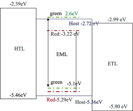
Fig.4 The energy level diagram of host or guest in emissive layer
2.2 Normalized electroluminescence spectra and chromaticity coordinate
Fig.5 shows the current density-chromaticity coordinate characteristics of the white OLEDs fabricated. It can be seen that from the Fig.5, the device color coordinates CIEx gradually decreased, while the CIEy remained stable with the increase of current density. Fig.6 shows the EL spectrum for devices. As can be seen from Fig.6(a), as the current density increase, the luminous intensity of blue, green and red appear to change. And compared with the red intensity, the luminous intensity of blue and green gradually increased. As far as we know, the emission in host-guest of co-doping system is considered to involve two emission mechanisms, energy transfer and carrier trapping. For an efficient energy transfer, it requires a significant spectral overlap between the photo-luminescent (PL) spectrum of the host and the absorption spectrum of the dopant. While for efficient carrier trapping, the highest occupied molecular orbital (HOMO) or lowest unoccupied molecular orbital (LUMO) energy level of the dopant must fall within that of the host. There are both electron and hole trapping for red guest, electron trapping for green guest in Fig.4. In this carrier trapping controlled device, electrons and holes are respectively trapped by the low-energy dopant under a low bias and the traps are gradually filled with the increasing electric field, resulting in a faster increase of the current [this case is usually called trap charge limited current (TCLC)][6]. Until all traps are filled, the current starts to increase more slowly [known as space-charge limited current (SCLC)]. In our doping system, carrier trapping is one of key factors that brings the color stability problem in WOLEDs as the driving voltage or current increases. From the above results, we can see that the emission intensity ratio of the dopant to the host changes in device, this means there also exists a good overlap between the emission of the blue light host and the absorption of the green, or red light guest, the emission from such a WOLED system include both carrier trapping and energy transfer mechanisms, and in such a situation a large change of the EL spectra or chromaticity occurs with the driving voltage or current.
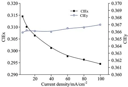
Fig.5 The relation between the current density and chromaticity coordinate of white organic Light emitting devices
2.3 Chromaticity coordinates shift mechanism
In order to further systematically analyze the chromaticity coordinates shift mechanism of organic white emitting light devices, the integral area of normalized electroluminescence spectra of devices at different current density were calculated, the proportion accounting for the integral area of blue+green and red were respectively obtained, and the detailed experimental results were listed in table 1. From the table, one can see that the integral area and the proportion of normalized EL spectra of clue+green gradually increase, at the same time the integral area and the proportion of red gradually decrease according to the change of the current density from 5~100 mA·cm-2. In addition, the experimental results indicate that the variation trend of the integral red area and proportion is consistent with color coordinate values CIEX, which make out the chromaticity coordinates shift of organic white light top-emitting devices in this co-doping system is mainly related to the variation of red percentage in white normalized EL spectra, and give rise to CIEX value change with the current density increase. From the relation between the red electroluminescence intensity and drive voltage in Fig.7, it can be found that the red portion in white normalized EL spectra of OLED devices linearly decrease with the drive voltage increase.
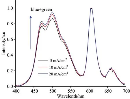

Fig.6 The normalized electroluminescence spectra of OLEDs at different current density
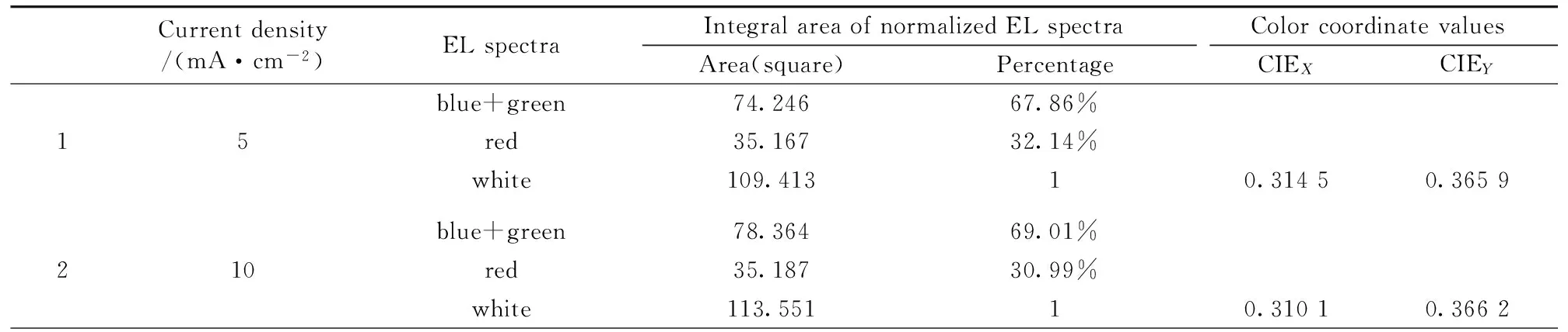
Table 1 The Integral area of normalized electroluminescence spectra at different current density and color coordinate values
To Table 2
blue+green80.93969.71%320red35.16930.29%white116.10810.30640.3661blue+green85.08771.16%440red34.48328.84%white119.57010.30120.366blue+green85.11971.41%560red34.07428.59%white119.19310.29770.3665blue+green85.04971.69%680red33.58628.31%white118.63510.29630.3666blue+green85.04072.11%7100red32.89527.89white117.93510.29450.367

Fig.7 The relation between the red electroluminescence intensity and drive voltage
In co-doping system of single-EML WOLEDs, when the electron and hole are trapped by the low-energy dopant under the low bias or current density, the energy transfer between the host and guest can not be effectively performed, and the electroluminescence intensity of host and guest do not simultaneously proportionally increase, which bring about the chromaticity coordinates shift of organic white light top-emitting devices with the variation of voltage or current density. Some previous research results also showed that if electron and hole are trapped by dopant[7-8], the luminous intensity of dopant will be restrained at different voltage, and it is difficult to distinguish the contribution of color evolution which the electron or hole bring about, this also hinder us to further clarify the mechanism behind the problem that result in the chromaticity coordinates shift of organic white light top-emitting devices with the variation of voltage or current density. On the other hand, the dopant luminescence can be divided into two parts, one originate from the energy transfer between host-guest system, and other come from the exciton trapped by dopant, it is also difficult to distinguish which one is the predominant contribution.
On account of the LUMO energy level of dopant is low than host, some electron trapping will come into being in dopant, so the dopant molecule captured carriers will lose opportunity to accept energy transfer and radiate. Base an the boltzmann distribution law, the specific value of the trapped electron number (Nt) by dopant at LUMO energy level and the free electron number (Nf) at LUMO energy level of host can be expressed as
(2)
WhereNdopantandNhostrespectively stand for the molecular number of host and dopant. If the electron charge isQ,Nfcan be described as the following equation
Nf=jST/Q=jSL2/μVQ
(3)
whereLis thickness of OLEDs,μis represents the electron mobility,Vis the driving voltage applied to the device. According to the space-charge-limited currents (SCLC), the relation between the current and voltage in insulator with shallow level trap can be written as
j∝μV2
(4)
Fromtheaboverelationship,itcanbeobtained
Nf∝V
(5)
andtherelationbetweenthedopantmolecularnumbertrappingelectronandthedrivingvoltageappliedtothedevicecanbeacquired.Asfarasweknow,thedopantmolecularacceptingenergytransferfromhostandthecorrespondinghostmoleculararenotoverlapbetweenthemintheco-dopingsystemofsingle-EMLWOLEDswithlowdopantconcentration,wellthentheelectroluminescenceintensityofdopantisproportionaltothedopantmolecularthatcanacceptenergytransferfromhost.Forthereasonthattheelectroluminescenceintensityofdopantcanbewrittenas
I=A-BV
(6)
WhereAandBis positive constant. From the above relation, it is can be found that the electroluminescence intensity of dopant linearly decrease in line with the driving voltage applied to the device, the theoretical results is completely consistent with the experimental one in Fig.5, the relation between the electroluminescence intensity of dopant and the driving voltage applied to the device is linearly fitted, it is can be seen that the fitting line is well matched with the experimental results, and obtainingAandBvalue is respectively 19.41 and 2.31 from the function.
3 Conclusion
In summary, the top emission organic light-emitting devices were fabricated by the thermal evaporation of the organic materials on (Al/Mo/MoO3) multi-layers anode, by doping the red and green guest into the blue host as emissive layer to prepare WOLEDs. Experimental results showed that according to the current density increase the luminous intensity of blue, green and red appear to change. Compared with the red intensity, the luminous intensity of blue and green gradually increased. And the emission in this host-guest co-doping system is considered to involve two emission mechanisms, energy transfer and carrier trapping, energy transfer and carrier trapping between the host-guest should be responsible for chromaticity coordinates shift of organic white emitting light devices, and it is proved the electroluminescence intensity of dopant linearly decrease in line with the driving voltage applied to the device by theoretical and experimental results.
[1] Tang C W, Vanslyke S A. Appl. Phys. Lett., 1987, 51(12): 913.
[2] Kido J, Kimura M, Nagai K. Science, 1995, 267: 1332.
[3] Wang Fengxia, Qiao Xianfeng, Xiong Tao, et al. Organic Electronics, 2008, (9): 985.
[4] Zhao Fangchao, Zhang Zhiqiang, Liu Yipeng, et al. Organic Electronics, 2012,(13): 1049.
[5] Jou Jwo-Huei, Chen Po-Wei, Chen Yu-Lin, et al. Organic Electronics, 2013,(14): 47.
[6] Du Xiaoyang, Huang Yun, Tao Silu, et al. Dyes and Pigments, 2015,(115): 149.
[7] Lee Jonghee, Lee Joo-Won, Cho Nam Sung, et al. Current Applied Physics, 2014, (14): 84.
[8] Kim Nam Ho, Kim You-Hyun, Yoon Ju-An, et al. Journal of Luminescence, 2013, (143): 723.
O461.2
A
顶发射白光OLED器件制备及其色坐标漂移机制研究
王光华1,2, 赵惠琼1,2, 邓荣斌1, 段 瑜1,2, 孙 浩1, 张筱丹1,2, 周 琴1, 钱金梅1, 万锐敏1,2, 季华夏1, 姬荣斌2
1. 云南北方奥雷德光电科技股份有限公司,云南 昆明 650223 2. 昆明物理研究所,云南 昆明 650223
采用了高反射率金属Al和电化学性能稳定的金属Mo,在硅基底上制备了多层结构的 Al/Mo/MoO3阳极,并研究了不同MoO3厚度下多层阳极的反射率。在此基础上,通过发光层共掺杂制备了顶部发光OLED器件,并对器件发光机制进行了系统研究和分析。实验结果表明: 采用发光层共掺杂制备的顶部发光OLED器件的色坐标,随电流密度或电压的增加而发生漂移;OLED器件色坐标漂移的原因是三基色发光强度随电流密度的增加,逐渐偏离了形成白光(0.33, 0.33)所需三基色强度比例值,导致了OLED器件的色坐标发生了漂移,其机制是发光层中主-客之间能量转移和陷阱共同作用的结果。进一步研究发现,在不同电压下,红光发光强度随驱动电压(或电流密度)增大而线性地减小。
有机电致发光器件;色坐标漂移;能量转移;陷阱
2015-11-06,
2016-03-21)
Foundation item: The National Natural Science Foundation of China(61604064), The General Program of Applied Basic Research (2016FB112) of Yunnan
10.3964/j.issn.1000-0593(2016)11-3758-06
Received: 2015-11-06; accepted: 2016-03-21