BaTi2Bi2O的电子结构与磁性
2015-11-30王广涛张会平
王广涛,张 琳,张会平,刘 畅
(河南师范大学物理与电子工程学院,河南新乡 453007)
文章编号:1001⁃246X(2015)01⁃0107⁃08
BaTi2Bi2O的电子结构与磁性
王广涛,张 琳,张会平,刘 畅
(河南师范大学物理与电子工程学院,河南新乡 453007)
采用第一性原理方法,对BaTi2Bi2O的电子结构和磁性进行计算.非磁性态的计算结果显示:费米能级处的态密度主要来自dz2,dx2-y2和dxy三个轨道,同时费米面也主要有三部分组成,并且将其沿着矢量q1=(π/a,0,0)和q2=(0,π/a,0)平移时,第三部分费米面(沿着X⁃R连线)与第一部分费米面(M⁃A连线)嵌套明显,计算得出磁化系数χ0(q)在X点出现峰值,与峰值出现在M点的FeAs基超导体不同.上述磁化率峰值可以诱导产生自旋密度波,使得BaTi2Bi2O材料的磁性基态是bi⁃collinear antiferromagnetism(AF3)与blocked checkerboard antiferromagnetism (AF4)的二度简并态.随着空穴掺杂,χ0(q)的峰值降低,而电子掺杂则导致峰值变大.当自旋涨落被完全压制时,超导出现,这可以解释为什么超导只出现在空穴掺杂型化合物而非电子掺杂型.
第一性原理;费米面嵌套;超导
0 引言
高温铁基超导体[1]的发现,引发了一轮新的探寻层状超导体(SC)的热潮,研究者旨在探寻那些与之有相似电子结构的材料,如LaCo2B2化合物[2]和BiS2基化合物[3].在探索新的超导体系的过程中,最理想的是像铁基超导体[1,4]那样,具有自旋密度波(SDW)不稳定性或者电荷密度波(CDW)不稳定性(由费米面嵌套导致)的层状结构材料.这是由于在结晶材料中超导态和自旋密度波态是两个相互关联又相互竞争的集合电子现象.自旋密度波态通常出现在二维体系中,该体系中存在费米面嵌套导致的自旋或电荷调制[5]现象.超导也可以被看做是另一种基于库伯配对效应的费米面不稳定性.超导态与自旋密度波态之间,通常是相互竞争又相互关联的[6].
近来Yajima等人[7]在BaTi2Bi2O材料中发现了超导(T c=1.2 K),并且其在50 K时发生类似于自旋密度波的相变.Doan等人[8]进一步发现,通过用钠原子替代Ba原子而进行空穴掺杂,其超导转变温度T c可以升高至5.5 K,同时自旋密度波转变温度降低至30 K左右.截至目前,理论与实验结果均显示Na2Ti2Sb (As)2O[9-11]、BaTi2As2O[12,16]、Ba2Ti2Fe2As4O[12]和 BaTi2Sb2O[13-14]中可能存在自旋密度波,通过观察Na2Ti2Sb2O的光谱学结果[11],以及BaTi2Sb2O的电声耦合的结果[13],人们已经证实了电荷密度波相转变的存在,以上这些发现都需要我们对SDW以及它与SC之间的关系作进一步的探究.本文用第一性原理研究Ba(1-x)NaxTi2Bi2O的电子结构、磁性和费米面嵌套情况.
1 研究方法
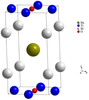
图1 BaTi2Bi2O非磁性态的晶体结构Fig.1 Structure of BaTi2Bi2O
计算采用基于超软赝势和平面波方法的STATE(Simulational Tool for Atom TEchnology)软件包[21].选用的晶格参数和原子位置都来自于XRD数据[15],晶体结构如图1,其中晶格常数为a=b=4.123 2Å,c =8.344 7Å,原子内部坐标为Ba(1d):0.5,0.5,0.5;Ti(2 f):0.5,0,0;Bi(2g):0,0,0.748 7;O(1c):0.5,0.5,0.为了探索材料真正的磁性基态,我们讨论六种不同的情况:非磁态(即无自旋极化态)、铁磁态以及四种不同的反铁磁态.对于这种磁性态,我们没有优化其结构,而是用用实验得到的非磁态结构进行的计算.第一种反铁磁类型,其最近邻的Ti原子自旋方向相反(如图2(a)),我们称为 checkerboard型反铁磁(AFM1);第二种反铁磁类型中,由Ti原子构成的正方形点阵的对角线上两原子自旋方向均相反(如图2(b)),我们称之为collinear型反铁磁(AF2);第三种反铁磁沿着由Ti原子构成的正方形点阵的一条对角线方向是铁磁态,而另一个对角线方向是反铁磁态(如图2(c)),称为bi⁃collinear[17]型反铁磁(AF3);第四种反铁磁如图2(d),Ti2Bi2O层被浅色窄虚线分成2×2的正方形点阵,其内部磁性态一致,相邻正方形内磁性态相反,并且其磁性单胞在ab面是一个2a×2a的正方形点阵,我们称这种反铁磁类型为blocked checkerboard型反铁磁(AF4).为了保证体系收敛,我们采用340 eV的截断能和20×20×10的K点网格数,用以优化交换关联能的广义梯度近似(GGA)[23]以PBE的形式应用于我们的计算中,Ti⁃3d态的电子关联性采用GGA+U[18]的方法处理.
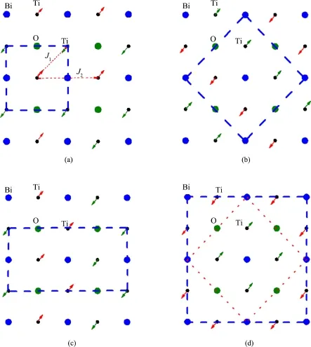
图2 Ti2Bi2O层俯视图(a)AF1,(b)AF2,(c)AF3,(d)AF4(其中虚线框代表ab面上不同反铁磁构型的磁单胞,不同原子种类和Ti原子磁性方向已在图中标出.图(a)中的J1和J2分别表示紧邻和次近邻交换常数.)Fig.2 Schematic top view of Ti2Bi2O layer(a)AF1,(b)AF2,(c)AF3,(d)AF4 (The dashed lines correspond tomagnetic unit cells of the different antiferromagnetic configurations. Atoms and directions of Timagneticmoments are denoted in the figure.)
2 结果与讨论
图3描绘了由GGA方法计算所得的BaTi2Bi2O非磁态的总的态密度(DOS)和分态密度,从图3(a)中我们可以看出每个化学单胞的费米能级处的态密度为N(EF)=3.42 state·eV-1,通过费米能级处的态密度可以计算得出,相应磁化率为:χ0(q)=1.1×10⁻⁴emu·mol-1,比热系数为:γ0=8.2 mJ·(K2·mol)-1,这与Suetin[16]的研究结果一致(χ0(q)=1.1×10⁻⁴emu·mol-1,γ0=8.06 mJ·(K2·mol)-1).另外由图可以看出,O⁃2p轨道的电子主要分布在从-7.4 eV到-4.7 eV的能量区域,从-5 eV到-1 eV的能量范围内,Bi⁃6p轨道的电子对态密度的贡献最大,Ti⁃3d轨道的电子形成的能带主要位于-4 eV~-1 eV之间,在费米能级处(由-1 eV到1 eV)主要分布着Ti⁃3d轨道的电子和与之有着强烈杂化的Bi⁃6p态电子,它们对于费米面的贡献分别是83%和17%.为了研究轨道特征,图3(b)给出了Ti原子3d态的5个分态密度,该图显示费米能级处的态密度主要是由Ti原子3d态的dz2,dx2-y2和dxy轨道电子贡献的,这一点与LaOFeAs[19]材料不同,后者费米能级处主要分布着dxy,dyz和dzx轨道的电子.它与Fe⁃As基超导体[24]不同的轨道特征,预示着两者的超导电子配对也是不同的.
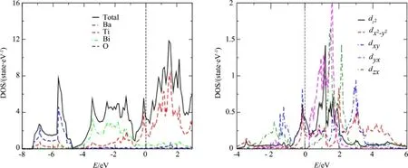
图3 (a)BaTi2Bi2O的态密度图及(b)Ti⁃3d态的投影态密度图Fig.3 (a)DOS of BaTi2Bi2O and(b)projected density of state of Ti⁃3d
从投影能带结构图(图4)可以看出,有两条能带穿越费米面,与BaTi2Sb2O[14]的轨道特征很相似,该图中穿越费米面的这两条能带是由Ti原子的dz2,dx2-y2和dxy态电子构成的,这点与Ti的投影态密度图(图3)吻合.图5描绘了三维费米面及在KZ=0,π/2,π/3处截取的费米面横截面.费米面有三部分构成,第一部分是沿着M⁃A连线(位于布里渊区的四个角).这一部分费米面显示出良好的二维特性,而图4(a)⁃(c)的投影能带结构图显示,这一部分的费米面主要是由Ti原子3d态中dz2,dx2-y2和dxy轨道的电子构成.第二部分位于布里渊区的中心位置(沿着Γ⁃Z连线),这部分费米面拥有复杂的三维形状,结合图4(a)可知其有明显的dz2轨道特征.此外费米面的第一部分与第二部分来自于同一能带.在费米面包括的区域内,载流子数量分别为0.248 electrons·cell-1和0.248 holes·cell-1,电子与空穴的浓度均为1.70×10²¹·cm-3.围绕着X点的第三部分属空穴型费米面,由于载流子中电子空穴各占一半,这部分费米面正好补偿了电子型费米面部分.与电子型费米面(第一部分费米面)相同,这部分费米面拥有dz2,dx2-y2和dxy的混合特征,其中dz2轨道特性尤为显著.
为了观察费米面的分布及其嵌套情况,我们分别截取了KZ=0、π/2、π/3时的费米面(图5).我们将费米面沿着矢量q1=(π/a,0,0)或者q2=(0,π/a,0)平移后,位于N点(0,π/a,0)的第三部分费米面(空穴型)与位于M点(π/a,π/a,0)的第一部分费米面(电子型)发生强烈嵌套(图5(c)).如果费米面在某个晶格震动矢量q的平移下(这不是一个物理过程,是一个理论上假想的平移)能够与原先的费米面基本重合,则这两个电子态就会受到该晶格震动模式的散射,发生简并微扰,同时打开能隙.而一旦能隙因此打开,能隙底部的态往往都是驻波态,并且具有相同的波动周期(因为它们是两个被晶格动量向连接的态的线性组合,这种组合的波函数在振幅上的波动必然与晶格的波动吻合).由于费米面上的态都是能级简并的,大量这样的电子态被费米子占据以后整个费米液体就会体现出密度波动,这就强化最初造成密度波动的涨落.这种正反馈就是费米面失稳的根本机制.先前对Fe基超导体的研究已经证实了:费米面的嵌套是导致SDW态主要原因[4,20].
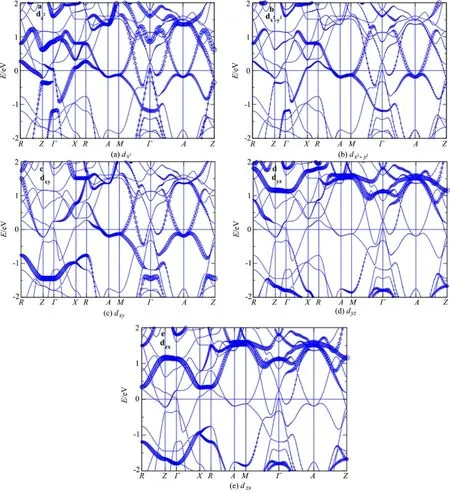
图4 BaTi2Bi2O的投影能带图(图中符号大小对应于布洛赫态在dz2、dx2-y2、dxy、dyz和dzx轨道上的投影比重.)Fig.4 Projected bands of BaTi2Bi2O(Symbol sizes correspond to projected weights of Bloch states onto dz2,dx2-y2,dxy,dyzand dzxorbitals.)
费米面嵌套效应可以由林哈德效应函数量化表示出来.对于无掺杂化合物,χ0(q)的峰值出现在X点(如图6(a)),强嵌套效应的存在暗示某种有序(比如SDW或者CDW[4,20])可能在低温无掺杂化合物(如LaOFeAs[4,20])中形成.我们通过将费米面上移0.2 eV来研究0.3个电子掺杂型的化合物的磁化率,同理,通过下移0.1 eV来研究0.3个空穴掺杂型化合物的χ0(q).对化合物进行0.3个空穴掺杂时(Ba0.7Na0.3Ti2Bi2O,图6(b)),χ0(q)的峰值降低,并且位置由X点向Γ点方向移动.这种现象曾在Fe⁃As基超导材料[24]中报导,其磁化率峰值(在M点)随着空穴掺杂明显降低并且变得有些不对称.然而对化合物进行0.3个电子掺杂时,χ0(q)却升高了,这与Fe⁃As基超导材料完全不同:首先,后者的磁化率峰值在非掺杂情况下出现在M点(并非X点),随着电子或空穴的掺杂明显降低并且略有不对称[24].我们的结果暗示,只有空穴掺杂才能将那些可以诱导SDW的费米面嵌套效应显著的压制.当SDW被完全压制时,超导便出现了.这些正好可以解释,为什么超导只能出现在空穴掺杂型化合物里而非电子掺杂型中.
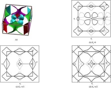
图5 (a)三维费米面图及费米面在(b)KZ=0、(c)π/2、(d)π/3处的横截面(实线是最初计算所得的费米面,虚线表示沿着矢量q=(π,0,0)平移之后的费米面.)Fig.5 (a)3D Fermi surfaces and cross⁃sections of Fermi surfaces(2D)at(b)KZ=0,(c)KZ=π/2,and(d)KZ=π/3 (Black lines are calculated Fermi surfaces,while greg lines indicate Fermi surfaces shifted by q=(π,0,0).)
强烈的嵌套效应会诱导产生自旋密度波,所以我们分别研究了材料的铁磁态和四种不同的反铁磁构型.早前的研究显示,Ti氧化物的电子关联性很重要[21],所以也考虑了 Ti⁃3d态的电子强关联性(GGA+U[22-23]).加U值从0到3 eV(如图7(b)),材料铁磁态的Ti原子磁矩均为0,由此知其与NM态简并.不加U时,AF1态、AF2态都和FM态(或者NM态)有相同的总能量(如图7(a)).同时以上3个态的Ti原子的磁矩均为0(如图7(b)).这就意味着在不考虑Ti原子电子关联性的情况下,FM态、AF1态和AF2态都与非自旋极化态简并.这个结果与Sing等人[20]关于BaTi2Sb2O的研究结果相同,后者发现以上各态都是不稳定的.另一方面,我们的研究结果与Lu等人[10]关于NaTi2Sb2O的结论(以上三个态均与NM态简并)也一致.对于AF3态和AF4态来说,与Fe⁃As基超导材料[1,20]的2μB相比,前者Ti原子磁矩小至0.13μB(Ueff=0 E). AF1态、AF3态和AF4态的能量随着加U而升高,其中AF3态和AF4态的Ti原子的磁矩由0.13μB(Ueff=0 eV)升高至0.82μB(Ueff=3 eV).正如上面所提到的,体系存在两个相互独立且相互正交的等效嵌套矢量q1=(π/a,0,0)和q2=(0,π/a,0).可能存在的自旋密度波将会在Ti⁃Ti正方形点阵内以M cos(q·R)的形式振荡,其中,R和M分别代表格点矢量和磁矢量.对应波矢量q=q1+q2和q1(q2),我们最终发现两个稳定的磁有序态即blocked checkerboard antiferromagnetic有序和bi⁃collinear antiferromagnetic有序.根据海森堡模型我们可以由这种磁性态的能量求得近邻和次近邻交换常数(如图7(c)).由交换常数均为负数,可以说明体系为什么更倾向于呈反铁磁态.
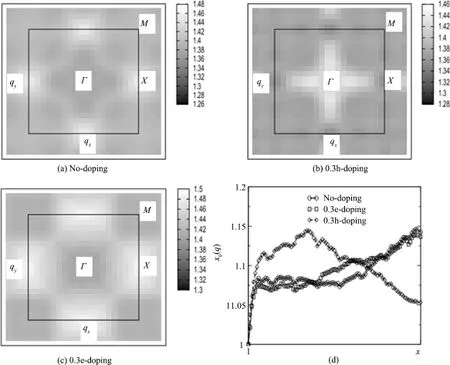
图6 计算所得的各个磁化系数χ0(q)图:(a)无掺杂情况、(b)0.3空穴掺杂情况、(c)0.3电子掺杂情况以及(d)三种掺杂情况下沿Γ-X线的情形Fig.6 Calculated bare susceptibility(Lindhard response function)χ0(q)at KZ=0,(a)without doping,(b)with 0.3 hole⁃doping,(c)with 0.3 electron⁃doping and(d)they alongΓ-X line
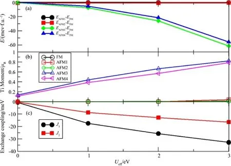
图7 (a)四个反铁磁态(AFM1、AFM2、AFM3、AFM4)相对于FM态的总能量,(b)随着加U增加,五种构型中Ti原子磁矩的变化;(c)近邻(J1)和次近邻(J2)交换常数随U变化Fig.7 (a)Total energies(with respect to FM state)of the checkerboard AF(AF1),collinear AF(AF2),bi⁃collinear AF(AF3),and blocked checkerboard AF(AF4),(b)Moments of Ti atoms in magnetic configurations as functions of electron correlation U,(c)First and second nearest neighbor exchange coupling constants as functions of U
3 结论
通过第一性原理计算研究了BaTi2Bi2O材料的电子结构和磁性.在非自旋极化态构型中,费米能级处的态密度主要由dz2,dx2-y2和dxy轨道的电子构成,这一点与Fe⁃As基超导材料不同.计算所得磁化率χ0(q)的峰值出现在X点,不像Fe⁃As基超导材料那样出现在M点.空穴掺杂使得χ0(q)的峰值降低并且略微有些不对称,而电子掺杂则使得该峰值升高.当SDW被完全压制时,超导便出现了.这些正好可以解释,为什么超导只能出现在空穴掺杂型化合物里而非电子掺杂型中.上述磁化率峰值诱导产生自旋密度波,使得BaTi2Bi2O材料的磁性基态是bi⁃collinear antiferromagnetism(AF3)与blocked checkerboard antiferromagnetism(AF4)的二度简并态.
[1] Kamihara Y,Watanabe T,Hirano M,Hosono H.Iron⁃based layered superconductor La[O1-xFx]FeAs(x=0.05-0.12)with Tc=26 K[J].Am Chem Soc,2008,130:3296-3297.
[2] Mizoguchi H,Kuroda T,Kamiya T,Hosono H.LaCo2B2:A Co⁃based layered superconductor with a ThCr2Si2⁃type structure [J].Phys Rev Lett,2011,106:237001-237004.
[3] Mizuguchi Y,Demura S,Deguchi K,Takano Y,Fujihisa H,Gotoh Y,Izawa H,Miura O.Superconductivity in novel BiS2⁃based layered superconductor LaO1-xFxBiS2[J].Phys Soc Jpn,2012,81:114725-114729.
[4] Dong J,Zhang H J,Xu G,Li Z,LiG,Hu W Z,Wu D,Chen G F,Dai X,Luo JL,Fang Z,Wang N L.Competing orders and spin⁃density⁃wave instability in La(O1-xFx)FeAs[J].Europhysics Letters,2008,83:27006-27009.
[5] Zhai H F,et al.Growth and characterizations of Ba2Ti2Fe2As4O single crystals[J].Phys Rev B,2013,87:100502-100506.
[6] Chen H,et al.Coexistence of the spin⁃density wave and superconductivity in Ba1-xKxFe2As2[J].Europhysics Lett,2009,85:17006-17018.
[7] Yajima T,Nakano K,Takeiri F,Ono T,Hosokoshi Y,Matsushita Y,Hester J,Kobayashi Y,Kageyama H. Superconductivity in Ba1-xKxTi2Sb2O(0≤x≤1)controlled by charge doping[J].JPhys Soc Jpn,2012,81:103706-103709.
[8] Doan P,et al.Growth and characterizations of Ba2Ti2Fe2As4O single crystals[J].Am Chem Soc,2012,134:16520-16523.
[9] Liu R H,et al.Physical properties of the layered pnictide oxides Na2Ti2P2O(P=As,Sb)[J].Phys Rev B,2009,80:144516-144520.
[10] Yan XW,Lu Z Y,Layered pnictide⁃oxide Na2Ti2Pn2O(Pn=As,Sb):A candidate for spin density waves[J].J Phys Condens Matter,2013,25:365501-365509.
[11] Huang Y,Wang H P,WangW D,Shi Y G,Wang N L.Formation of the density wave energy gap in Na2Ti2Sb2O:An optical spectroscopy study[J].Phys Rev B,2013,87:100507-100510.
[12] Sun Y L,et al.Growth and characterizations of Ba2Ti2Fe2As4O single crystals[J].Am Chem Soc,2012,134:12893-12897.
[13] Subedi A.Electron⁃phonon superconductivity and charge density wave instability in the layered titanium⁃based pnictide BaTi2Sb2O[J].Phys Rev B,2013,87:054506-054511.
[14] Wang G T,Zhang H P,Zhang L,Liu C.The electronic structure and magnetism of BaTi2Sb2O[J].JAppl Phys,2013,113:243904-243908.
[15] Yajima T,Nakano K,Takeiri F et al.Tcenhancement by aliovalent anionic substitution in superconducting BaTi2(Sb1-xSnx)2O[J].JPhys Soc Jpn,2013,82:074707-074711.
[16] Suetin D V,Ivanovskiii A L.Electronic properties and fermi surface for new Fe⁃free layered pnictide⁃oxide superconductor BaTi2Bi2O from first principles[J].JETP letters,2013,97:220-225.
[17] Ma F J,JiW,Hu JP,Lu ZY,Xiang T.First⁃principles calculations of the electronic structure of tetragonal alpha⁃FeTe and alpha⁃FeSe crystals:Evidence for a bicollinear antiferromagnetic order[J].Phys Rev Lett,2009,102:177003-177007.
[18] Anisimov V I,Zaanen J,Anderson O K.Strong Coulomb correlations in electronic structure calculations[J].Phys Rev B,1991,44:943-954.
[19] Mazin I I,Johannes M D,Boeri L,Koepernik K,Singh D J.Problemswith reconciling density functional theory calculations with experiment in ferropnictides[J].Phys Rev B,2008,78:085104-085110.
[20] Xu G,Ming W,Yao Y,Dai X,Zhang S C,Fang Z.Doping⁃dependent phase diagram of LaO M As(M=V-Cu)and electron⁃type superconductivity near ferromagnetic instability[J].Europhysics Lett,2008,82:67002-67006.
[21] Solovyev I,Hamada N,Terakura K.Crucial role of the lattice distortion in the magnetism of LaMnO3[J].Phys Rev Lett,1996,76:4825-4828.
[22] Fang Z,Terakura K.Structural distortion andmagnetism in transitionmetal oxides:Crucial roles of orbital degrees of freedom [J].JPhys Condens Matter,2002,14:3001-3014.
[23] Perdew JP,Wang Y.Accurate and simple analytic representation of the electron⁃gas correlation energy[J].Phys Rev B,1992,45:13244-13249.
[24] Chen W Q,Yang K Y,Zhou Y,Zhang FC.Strong coupling theory for superconducting iron pnictides[J].Phys Rev Lett,2009,102:047006-047009.
0 Introduction
Recently,graphite⁃related materials such as fullerenes, carbon nanotubes, especially graphene,have been gradually attracted broad attention due to their unique electronic and excellent physical properties.It has been demonstrated that graphene,amonolayer of carbon atoms arranged laterally in a honeycomb lattice,as the most promising candidate material for nanoelectronic devices,owing to its remarkable high electron and hole mobility,combined with high mechanical and thermal stability[1-3].
Although two⁃dimensional graphene is a zero⁃gap material and makes it not suitable for transistor applications,it has been studied by researches that this problem can be circumvented by means of graphene nanoribbons(GNRs)due to quantum confinement in the width direction[4-6].The electronic properties of GNRs depend sensitively upon their widths and shape of edges.Semiconducting GNRs can be used as channel material[7-8]of field effect transistors(FETs)which have been explored as potential alternatives to CMOS devices.Compared with siliconmaterials,due to an exceptionally high mobility,and near ballistic transport in GNR,GNRFETs can obtain a higher driving current,faster operation speed and a significant reduction in power consumption[9-11].
In the recent past,gate underlap structures have been reported to reduce electric field in the drain of FETs and thus reduce interband tunneling in the drain which is the cause of ambipolar leakage current[12-14].In addition,linear doping in the underlap region is generally used to suppress band to band tunneling(BTBT)and ambipolar conduction of MOSFETs.In this structure,the n⁃type impurity is at maximum level at source/drain side and reduces linearly toward theintrinsic channelwhich becomes zero at end of channel at source/drain side.
On the other hand,to enhance the immunity against short⁃channel effects(SCE),triple⁃material⁃gate(TMG)structures have been proposed to improve the performances of GNRFETs[15]. Compared to a single⁃material⁃gate⁃GNRFET(SMG⁃GNRFET),TMG⁃GNRFET has three materials with differentworkfunctions laterallymerged together in gate.Due to the field discontinuity along the channel,this structure leads to potential steps along the channel at the interfaces of different gate metals.As the drain potential changes,the step in potential increases,which provides a better shielding of the channel from the drain variation,leading to a considerable increase in average carrier velocity in the channel.
In order to possess the advantages of both triple⁃material⁃gate and linear doping profile,we propose a compound structure called linear doping triple⁃material⁃gate GNRFET(TL⁃GNRFET).In this paper,based on a previous work[16],we investigated the characteristics of GNRFETs,using self⁃consistentmethod solving the non⁃equilibrium Green's function(NEGF)coupled with a three⁃dimensional Poisson equation under the ballistic limits in the mode space.By comparing the conventional single⁃material⁃gate GNRFET with conventional doping GNRFET(SC⁃GNRFET),single⁃material⁃gate GNRFET with linear doping(SL⁃GNRFET),triple⁃material⁃gate GNRFET with conventional doping(TC⁃GNRFET)and triple⁃material⁃gate with linear doping(TL⁃GNRFET),it indicates that TL⁃GNRFET structure simultaneously reduces the off⁃state current and has better switching performance.In addition,asymmetric gate underlap and its effects have also been discussed and it is revealed that a structure in which top and bottom gates are both shifted towards the source has an improved subthreshold performance.
1 Model and Methods
In order to simulate the device characteristics,we perform a self⁃consistent calculation of potential and charge density in GNRFET.To obtain the self⁃consistentpotential,a nonlinear Poisson equation is solved for double gated GNRFETs by setting Dirichlet boundary conditions on the gate surface and Von Neumann boundary conditions along the exposed surface of the dielectric.To describe characteristics of the GNRFET,we used a tight⁃binding Hamiltonian with the atomistic nearest neighbor pz⁃orbital tight binding approximation.The recursive Green function algorithm is used to solve the NEGF equations for the density of states,charge density,and current.The self⁃energy generated by device's source and drain electrode can be solved by calculating the surface Green function using iterative approach[16-18].
The calculation of charge density is using the NEGF[17-18].Retarded Green's function of the device is

whereη+is a positive infinitesimal,E is energy,HDis the Hamiltonian when electrons in GNR is under the best adjacent approximation,ΣSandΣDare self⁃energies generated by device's source and drain electrodes,which can be solved by calculating the surface Green function using iterative approach.Once we get the Green function,the density of electron and hole in any position in the device can be given by the following equations
where EIis partial Fermi level in GNR,EFD(S)is the Fermi level in drain(source).The electrostatic potential profile can be obtained by solving the 3D⁃Poisson equation when the electron and holes density have been computed and Eq.(2)and Eq.(3).Therefore,3D⁃Poisson equation is expressed as

where U is electrostatic potential,εis dielectric constant,ρis the distribution of net charge.To calculate the channel current,we can use the Landauer⁃Büttiker formula

where q is the electron charge,h is Planck's constant and T[E]=Trace[ΓGΓG+],which is the transmission coefficient of electron tunneling through the channel,EFD(S)is Fermi level of the drain (source).
In summary,the Poisson⁃Schrödinger self⁃consistent algorithm in this paper can be simplified as follows(as shown in Fig.1):
(a)Give the initial value of electrostatic potential of the device;
(b)Solve the NEGF equations for device specified to obtain the charge density Eqs.(2)-(3);
(c)Put Eqs.(2)-(3)into Poisson Eq.(4)to obtain a new electrostatic potential;
(d)Repeat step(b)and(c)until the convergence of electrostatic potential and charge density is achieved;
(e)Put the convergence solution into the NEGF to obtain channel current(5).
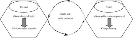
Fig.1 Poisson⁃Schrödinger self⁃consistent algorithm
2 Results and discussions
Simulation results are presented for double⁃gate GNRFET structure made from armchair GNR with N=13(width of 1.47 nm and bandgap of Eg≈0.72 eV).Double⁃gate geometry is implemented using SiO2as the gate insulator.Unless otherwisementioned,the basic parameters of SMG⁃GNRFET are thickness of gate oxide Tox=2 nm,n⁃doped GNR extensions length at source/drain ends Lsd=20 nm,dielectric constantof gate oxideε=3.9,the fraction of doping atoms in then+source/drain 5×10⁻³,length of gate Lg=10 nm,the channel GNR undoped.A schematic longitudinal cross⁃sectional view of TMG⁃GNRFET is shown in Fig.2.The gate of TMG⁃GNRFET consists of three laterally contacting metals M1,M2 and M3 with length LS,LMand LD,respectively.The work function of the main gate metal M2,unless otherwise mentioned,is larger than that of the two side gates M1 and M3 with the same metals.The rest parameters remain the same as the SMG⁃GNRFET.Transversal cross⁃section of the simulated GNRFET structure is shown in Fig.2(b),and the oxide layer thickness of the width direction S1=S2=1 nm.Different doping strategies are shown in Fig.2(a).Unless otherwisementioned,the length of underlap region Lu1=Lu2=10 nm.
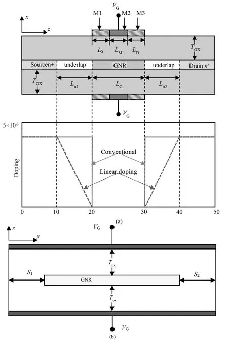
Fig.2 Simulated TMG⁃GNRFETs(A 50 nm⁃long armchair⁃edge GNR is used as channelmaterial.)(a)Longitudinal cross⁃section and doping profile,(b)Transversal cross⁃section
2.1 Comparison w ith experiment
Figure 3 shows a comparison of GNRFETs output characteristics ofmeasured and modeled[19]. The channel of the p⁃type GNRFET with back⁃gate topology is Lch=110 nm,the width of GNR is w ≈2.5 nm corresponding to 21⁃AGNR,and the SiO2,tox=10 nm.It is observed that our results arein good agreement with simulated results given in Ref. [20].However,due to the presence of elastic/inelastic scattering such as edge roughness scattering, optical phonon scattering and defect scattering which could limit the carrier transport of GNR channel,themeasured current is lower than the ballistic current of simulations for same device structure(A⁃GNR of 2.5 nm width and 110 nm channel length),as shown in Fig.3.As can be seen,the experimental GNRFET delivers about 20%of the ballistic current at low|Vds|and about40%of the ballistic current at high|Vds|.
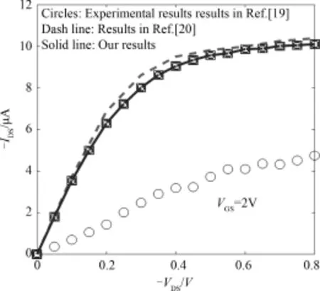
Fig.3 Output characteristics of GNRFET in our result,simulated ballistic result in Ref.[20]and experimental data adopted from Ref.[19]
2.2 Compound effects of linear doping and triple⁃material⁃gate structures for GNRFET
Here,the effects of gate length on the static performances of GNRFET structure are studied. Figure 4 shows transfer characteristics of SC⁃GNRFET with different length.It is clear that the SC⁃GNRFET with longer gate has better sub⁃threshold characteristic which indicates lower power consumption.This is because the effect of DIBL which is becomingmore significantwith decreasing gate length.
In order to study the impact of linear doping and hetero⁃material gate on the performance of GNRFETs,we compare the transfer characteristics of SMG⁃GNRFET and TMG⁃GNRFET with and without linear doping in Fig.5.The following observations are indicated from the figure:(1)The current characteristics of TC⁃GNRFET is similar with SC⁃GNRFET at the same drive current,while the off⁃state current and subthreshold slope of TC⁃GNRFET is found lower than SC⁃GNRFET.(2)Linear doping has improvement in the subthreshold characteristics of both SMG⁃GNRFETs and TMG⁃GNRFETs.(3)Compared to other structures,TL⁃GNRFET has a slightly lower on⁃state current and the lowest off⁃state current,that is to say,the Ion/Ioffof TL⁃GNRFET is the best.
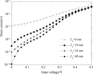
Fig.4 Transfer characteristics of SC⁃GNRFET,the gate length is 6,10,16 and 15 nm
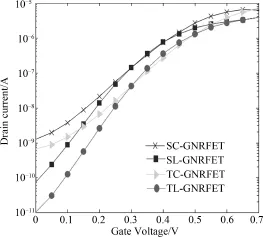
Fig.5 Transfer characteristics of GNRFETs with different structures
The subthreshold swing defined by S=d Vgs/d(ln I)is a key parameter of transistorminiaturization.A small subthreshold swing(S)is desired for low threshold voltage and low power operation for FETs scaled down to small sizes.Subthreshold swing of SC⁃GNRFET and SL⁃GNRFET and TL⁃GNRFET are compared in Fig.6.It is evident from the figure that,SC⁃GNRFET has the largest subthreshold swing,while TL⁃GNRFET has the smallest subthreshold swing.In reflects the TL⁃GNRFET has a better control ability for suppressing the SCE effect.
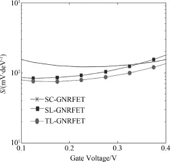
Fig.6 Threshold voltage swing of different GNRFETs at Vds=0.7 V
In addition,DIBL is an importantmanifestation of SCE effect.To study the DIBL in TL⁃GNRFET,Fig.7 illustrates the comparison of threshold voltage shift betweens C⁃GNRFET and TL⁃GNRFET as the drain voltage increases from 0.01 V to 0.7 V.Here,we define the threshold voltage corresponding to the gate voltage of 10 nA current of channel.As shown in Fig.7,threshold voltage shift of SC⁃GNRFET is 0.11 V while that of TL⁃GNRFET is 0.05 V,which indicates that TL⁃GNRFET has better ability in suppressing DIBL effect compared to convention GNRFETs.It can be explained by electronic potential along channelwith different drain voltage of TL⁃GNRFET.It is clearly from Fig.8 that the increase of additional drain potential is absorbed under the gate near drain,while the gate near the source region is screened from drain potential variations.As a result,Vdshas only a small influence on drain current after saturation.Thus,the gate has better controlling over the channel and suppresses the DIBL effectively.
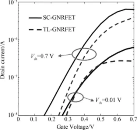
Fig.7 Shift in threshold voltage of SC⁃GNRFET and TL⁃GNRFET at Vds=0.01 V and Vds=0.7 V
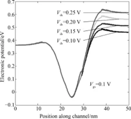
Fig.8 Potential profile along channel of TL⁃GNRFET at different drain biases
To probe physical mechanisms responsible for the improved performance of TL⁃GNRFET,lateral electric field profiles along channel of different GNRFET at Vgs=Vds=0.3 V are shown in Fig.9.Comparing Fig.9(a)and Fig.9(b),we found that the implantation of linear doping has a prominent effect on reducing electric field in the drain region,so the linear doping has a great contribution to preventing the hot carrier effects.Comparing Fig.9(a)and Fig.9(c),we found that as triple⁃material⁃gate is applied,the changes aremainly in the gate region.The triple⁃material⁃gate promotes the average electric field in the channel,and thus enhances the electron transportefficiency.In addition,the linear doping reduces the electric field in the drain aswell as that in the source,while the triple⁃material⁃gate enlarges the source region electric field.So the triple⁃material⁃gate can be an compensation in structures with linear doping as shown in Fig.9(d),enhancing the electron transport efficiency,keeping the source electric field relatively high,and less affecting electric field in the drain.The curves in Fig.9 proved the explanation.The structure with linear doping and triple⁃material⁃gate has the best subthreshold characteristics and on⁃off current ratio.
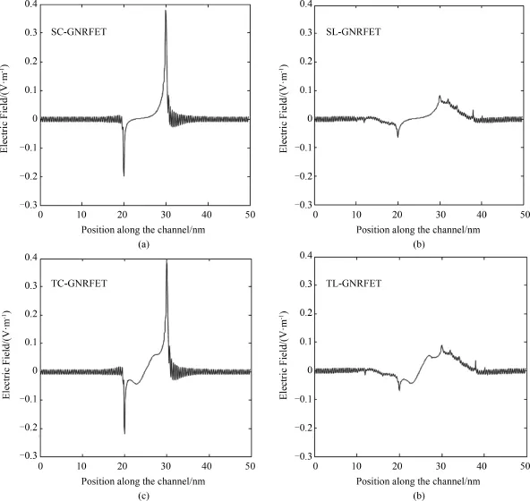
Fig.9 Electric field profiles along channel of different GNRFET at Vgs=Vds=0.3 V (a)SC⁃GNRFET(b)SL⁃GNRFET(c)TC⁃GNRFET(d)TL⁃GNRFET
2.3 Effects of asymmetric gate underlap
In this section,we investigate effects of source/drain asymmetric gate underlap and developed new GNRFET architectures aiming the optimization of transistor ambipolarity and on/off ratio Ion/Ioff.In traditional GNRFETs,the gate is
located in the middle of the device.We simulated situations that the top and bottom gates are both shifted towards the source(Asy.S)or the drain (Asy.D).And the linear doping single⁃material⁃gate(SL)and linear doping triple⁃material⁃gate (TL)structures are under investigation respectively,as shown in Fig.10.

Fig.10 Cross⁃sectional view of asymmetric gate GNRFET with different structures(a)Asy.S(b)Asy.D
To study the performance of asymmetric gate,comparisons are made between conventional doping and linear doping for SMG⁃GNRFET and TMG⁃GNRFET.The drain current versus gate voltage of SC⁃,SL⁃,T⁃,and TL⁃GNRFETwith Asy.Sstructure and Asy.D structure are plotted in Fig.11,respectively.It is obvious from Fig.11(a)that,as the top/bottom gatemoving towards the source,the four devices will have better subthreshold characteristics and smaller off⁃state current compared to the symmetrical gate structures(as shown in Fig.5).On the other hand,from Fig.11 (b),it is noticed that,the four devices have worse subthreshold characteristics and larger off⁃state current compared to the symmetrical gate structures(as shown in Fig.5),as the top/bottom gate moving towards the drain.
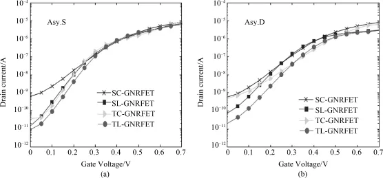
Fig.11 Transfer characteristics of different GNRFETs with misalignment toward source 5 nm
To see clearly the variation of Ionand Ioffof four deviceswith asymmetrical gate structures,three tables are shown.Comparing Tab.1 with Tab.2,we found that Ion/Ioffof four structures become larger as the top/bottom gatemoving towards the source.On the contrary,comparing Tab.1 with Tab.3,Ion/Ioffof four structures become smaller as the top/bottom gatemoving towards the drain.
The effects of the source/drain asymmetric gate underlap can be found in electron potential profiles shown in Fig.12.Comparing Fig.12(a)with Fig.12(c),as gates shift a certain part to drain region,the electron potential distributions between the channel and source becomesmore gentlethan that as gates shift a certain part to source region,which makes the off⁃state current of Asy.S structure greater than that of Asy.D.
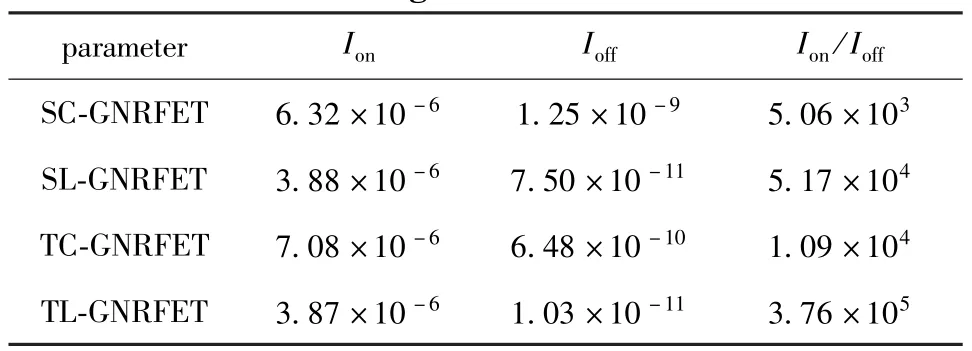
Table 1 On/off state current of four structures of GNRFETs w ith gate located in them iddle
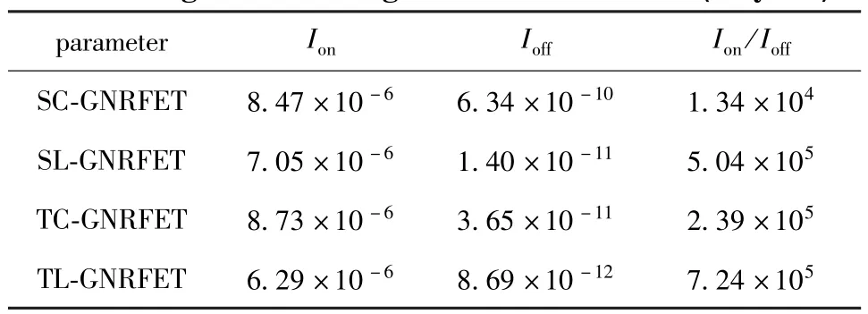
Table 2 On/off state current of four structures of GNRFETs w ith both gatemoved together towards source(Asy.S)
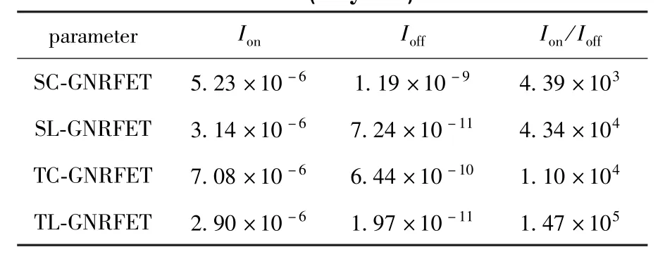
Table 3 On/off state current of four structures of GNRFETs w ith both gatem oved together towardsdrain(Asy.D)
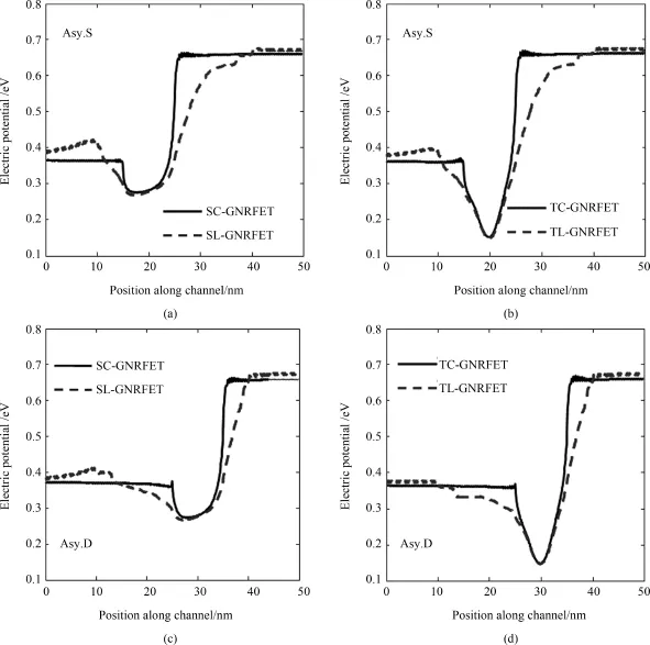
Fig.12 Electronic potential profiles along channel of different of GNRFET at VgsVds=0.3 V
It can be explained in other ways as well. Figure 13 shows lateral electric field distributions of the source/drain asymmetric gate underlap of GNRFETs.As the gate ismoving towards the drain,the electric field in the source region decreases,whilethat in the drain region has a great promotion,which is not ideal for nanoscale electronic devices. However,as the gate is located near the source,the source electric field is enhanced and there is a relatively wealer electric field in the drain region,and thus efficiently suppress the hot carrier effects.What ismore,in the channel region,the average electric field is the greatest as the gate is more near the source than the drain,which means in that situation the device has higher electron transport efficiency.In summary,as the gate locates near the source,the device has better performance.
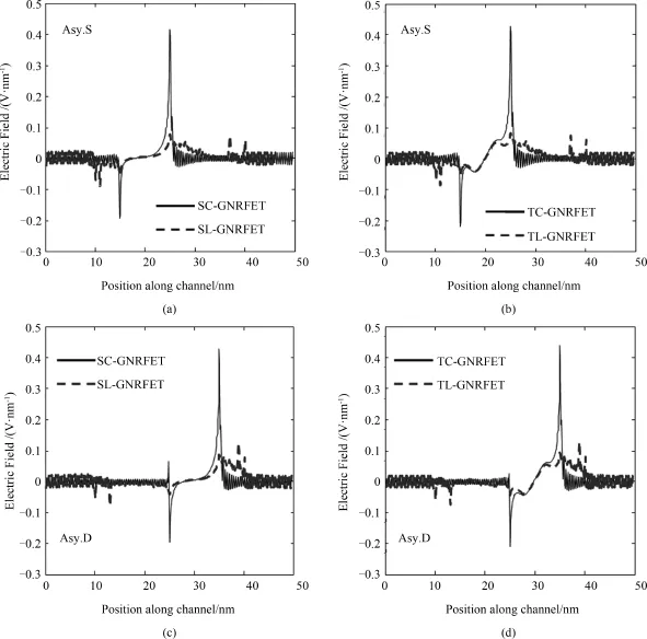
Fig.13 Electric field profiles along channel of different GNRFET with source/drain asymmetric gate underlap at Vgs=Vds=0.3 V,(a)and(b)Asy.S,(c)and(d)Asy.D
3 Conclusions
Based on a previous work,we investigated characteristics of GNRFETs,using self⁃consistent method solving the non⁃equilibrium Green's function(NEGF)coupled with a three⁃dimensional Poisson equation under the ballistic limits in themode space.By comparing TL⁃GNRFET with SC⁃GNRFETs,SL⁃GNRFETs and TC⁃GNRFETs,we find that the TL⁃GNRFET structure simultaneously reduces the off⁃state current and has better switching performance.In addition,the asymmetric gate underlap and its effects are discussed and it is revealed that the asymmetric structure in which the gate is located near the source has an improved on/off state current performance.
[1] Neto A H C,Guinea F,Peres N M R,Novoselov K S,Geim A K.The electronic properties of graphene [J].Rev Mod Phys,2009,81:109-162.
[2] Lemme M C,Echtermeyer T J,Baus M,Kurz H.A graphene field⁃effect device[J].IEEE Electron Device Lett,2007,28(4):282-284.
[3] George S.Gate capacitancemodeling and width⁃dependent performance of graphene nanoribbon transistors [J].Microelectron Eng,2013,112:220-226.
[4] Noei M,Moradinasab M,Fathipour M.A computational study of ballistic graphene nanoribbon field effect transistors[J].Physica E,2012,44(7-8):1780-1786.
[5] Li X L,Wang X R,Zhang L,Lee SW,Dai H J.Chemically derived,ultra smooth graphene nanoribbon semiconductors[J].Science,2008,319:1229-1232.
[6] Han M Y,Ozyilmaz B,Zhang Y B,Kim P.Energy band⁃gap engineering of graphene nanoribbons[J]. Phys Rev Lett,2007,98:206805-206808.
[7] Obradovic B,Kotlyar R,Heinz F,Matagne P,Rakshit T,GilesM D,Stettler M A,Nikonov D E Analysis of graphene nanoribbons as a channelmaterial for field⁃effect transistors[J].Appl Phys Lett,2006,88 (14):142102(3).
[8] Chen Z,Lin Y M,Rooks M J,Avouris P.Graphene nanoribbon electronics[J].Phys E,2007,40(2):228-232.
[9] Lin Y M,Dimitrakopoulos C,Jenkins K A,Farmer D B,Chiu H Y,Grill A,Avouris Ph.100 GHz transistors from wafer⁃scale epitaxial graphene[J].Science,2010,327:662-662.
[10] Liao L,Bai J,Cheng R,Lin Y C,Jiang S,Qu Y,Huang Y,Duan X.Sub⁃100 nm channel length graphene transistors[J].Nano Letters,2010,10(10):3952-3956.
[11] Liao L,Lin Y C,Bao M Q,Cheng R,Bai J,Liu Yuan,Qu Y,Wang K,Huang Y,Duan X.High⁃speed graphene transistorswith a self⁃aligned nanowire gate[J].Nature,2010,467:305-308.
[12] Alam K,Lake R.Role of doping in carbon nanotube transistors with source/drain underlaps[J].IEEE Trans Nanotechnol,2007,6(6):652-658.
[13] Kordrostami Z,Sheikhi M H,Zarifkar A.Influence of channel and underlap engineering on the high⁃frequency and switching performance of CNTFETs[J].IEEE Trans Nanotechnol,2012,11(3):526-533.
[14] Sarvari H,Ghayour R.Design of GNRFET using different doping profilesnear the source and drain contacts [J].International Journal of Electronics,2012,99(5):673-682.
[15] Orouji A A,Arefinia Z.Detailed simulation study of a dual material gate carbon nanotube field⁃effect transistor[J].Phys E,2009,41(10):552-557.
[16] Wang W,Yang X,Li N,Zhang L,Zhang T,Yue G.Numerical study on the performance metrics of lightly doped drain and source graphene nanoribbon field effect transistors with double⁃material⁃gate[J]. Superlattices and Microstructures,2013,64(9):227-236.
[17] Mintmire JW,White C T.Universal density of states for carbon nanotubes[J].Physics Review Letters,1998,81(12):2506-2509.
[18] Fiori G,Iannaccone G.Simulation of graphene nanoribbon field⁃effect transistors[J].IEEE Electron Device Letters,2007,28(8):760-762.
[19] Wang X,Ouyang Y,Li X,Wang H,Guo J,Dai H.Room⁃temperature all⁃semiconducting sub⁃10 nm graphene nanoribbon field⁃effect transistors[J].Phys Rev Lett,2008,100(20):206803-206807.
[20] Guo J.Modeling of graphene nanoribbon devices[J].Nanoscale,2012,4:5538-5548.
Electronic Structure and M agnetism of BaTi2Bi2O
WANG Guangtao,ZHANG Lin,ZHANG Huiping,LIU Chang
(College of Physics and Information Engineering,Henan Normal University,Xinxiang 453007,China)
Electronic structure and magnetic structures of BaTi2Bi2O are studied with first⁃principles calculations.In nonmagnetic state,density of states at Fermi level aremostly derived from dz2,dx2-y2and dxyorbitals.Fermisurface(FS)consists of three sheets. The third FS sheet(along X⁃R line)nestswith the first FS sheet(along M⁃A line)by q⁃vector q1=(π/a,0,0)or q2=(0,π/a,0)shift.Calculated bare susceptibilityχ0(q)peaked at X⁃point,rather than at M⁃point in FeAs⁃based superconductors.Such peaked susceptibility induces spin density wave(SDW).Magnetic ground state is nearly two degenerate antiferromagnetism of bi⁃collinear antiferromagnetism(AF3)and blocked checkerboard antiferromagnetism(AF4).Peak of susceptibilityχ0(q)is obviously suppressed and becomes slightly in⁃commensurate with hole doping,but increased with electron doping.As spin fluctuation is suppressed superconductivity appears.It explains that superconductivity appears only in hole⁃doped compounds,and not in electron⁃doped ones. Key words: first⁃principles calculations;Fermi surface nesting;superconductivity
Performance of Asymmetric Linear Doping Triple⁃material⁃gate GNRFETsWANGWei,GAO Jian,ZHANG Ting,ZHANG Lu,LINa,YANG Xiao,YUE Gongshu(College ofElectronic Science Engineering,Nanjing University of Post and Telecommunications,Nanjing,Jiangsu 210023,China)
GNRFET;NEGF;triple⁃gate⁃material;linear doping
O484.3 Document code:A
O469
A
2013-09-22;
2014-07-30
国家自然基金(11274095)和河南省高校创新人才(2012HASTIT009)资助项目
王广涛(1976-),男,博士,教授,从事第一性原理计算,E⁃mail:wangtao@htu.cn
Received date: 2013-09-22;Revised date: 2014-07-30
Received date:2014-01-25;Revised date:2014-06-26
Foundation item s:Supported by Natural Science Fouudation of Higher Eduction in Jiangsu Province(10KJD510006)
Biography:WangWei(1964-),male,PhD,associate professor,major in nanoelectronics,E⁃mail:wangwej@njupt.edu.cn
