Design of shared bus DSP board in vector network analyzer
2013-12-20LIUDanWANGBaorui王保锐
LIU Dan (刘 丹), WANG Bao-rui (王保锐)
(1. Science and Technology on Electronic Test & Measurement Laboratory, Qingdao 266555, China; 2. The 41st Institute of China Electronics Technology Group Corporation, Qingdao 266555, China)
Design of shared bus DSP board in vector network analyzer
LIU Dan (刘 丹)1,2, WANG Bao-rui (王保锐)1,2
(1. Science and Technology on Electronic Test & Measurement Laboratory, Qingdao 266555, China; 2. The 41st Institute of China Electronics Technology Group Corporation, Qingdao 266555, China)
Currently, the mainstream vector network analyzer employs embedded computer module with a digital intermediate frequency (IF) board to form a high performance windows platform. Under this structure, the vector network analyzer needs a powerful encoding system to arbitrate the bus acquirement, which is usually realized by field-programmable gate array (FPGA) chip. The paper explores the shared bus design method of the digital signal processing (DSP) board in network analyzer. Firsty, it puts an emphasis on the system structure, and then the shared bus communication method is described in detail; Finally, the advantages of the shared bus communication mechanism are summanzed.
shared bus; host port interface (HPI); external memory interface (EMIF); field programmable gate array (FPGA); peripherical component interconnect (PCI) interface device
CLD number: TM931 Document code: A
The vector network analyzer is an important instrument in the field of microwave measurement, which is widely applied in aviation, aerospace and various measurement fields. Currently, the mainstream vector network analyzer employs embedded computer module with windows operation system and adopts graphical operation interface which offers abundant interfaces and user friendly interfaces[1-3]. Moreover, the parameters of analyzer like measurement speed, measurement accuracy, measurement type, dynamic range, etc. have been further improved. Although computer module with windows system has refined task scheduling mechanism, flexible communication system and powerful graphical user interface (GUI), it tends to make real-time response to user’s operation and finish different communication requests. To meet the user demand for high efficient measurement, a single embedded computer module is not enough to perform real-time control to hardware and acquire measurement data. Therefore, a high performance vector network analyzer needs a digital intermediate frequency (IF) board to integrate the functions of controlling, acquisition and real-time data handling.
For the reasons mentioned above, the high performance vector network analyzer adopts multiple CPU architecture, which uses a high performance digital signal processor (DSP) with field-programmable gate array (FPGA) chip to build a DSP system that integrates controlling, acquisition and data handling functions to assist embedded computer with Pentium processor and to perform all the functions of vector network analyzers. This paper takes some high performance vector network analyzers as examples and describes the shared bus communication mechanism under this architecture.
1 System architecture of high performance vector network analyzer
The vector network analyzer uses embedded computer module and DSP to construct the master and slave CPUs, and uses Windows XP operation system as software platform. The analyzer system software is a standard windows installation program which can run right after installation.
For the master CPU of analyzer system, embedded technology extended (ETX) computer control module is named as host to realize user-machine interface functions including user interface, input/output, programming, data formatting, display, printing, storing, calibration and verification, etc. Taking floating point DSP chip of TI and high performance FPGA of Xilinx Company as the core, the digital IF processing board integrates the functions of controlling, acquisition, filtering and data processing. It communicates with the host in real-time to control the system hardware, sample data from IF and filter the data into needed form. Digital IF board is plugged in the peripheral component interconnect (PCI) slot of the host.
The host communicates with DSP via PLX9054 control chip. PLX9054 can work in various modes and it is suitable for PCI terminals with different transfer speeds. The speed of its local bus can reach 50 MHz and the data width can support 8, 16 and 32 bit[4]. To meet the control and high speed data transmission requirements of vector network analyzer and to increase measurement efficiency, DSP data bus on DSP board, FPGA data bus and PCI data bus use multiple bus multiplexing shared method and digital logic designed inside FPGA to complete bus arbitration and read-write control. The relationship of host and DSP is shown in Fig.1[5].

Fig.1 Connection diagram of DSP board and master CPU
2 Shared bus communication design
The C67x series floating point DSP chips of TI Company have the features of high calculation speed and large on-chip memory, and they supports various peripheral devices and industrial standard interface protocols, among which the external memory interface (EMIF) and the host port interface (HPI) provide convenience for designers to meet the requirements of connecting different peripheral devices and communicating with other CPUs[6,7].
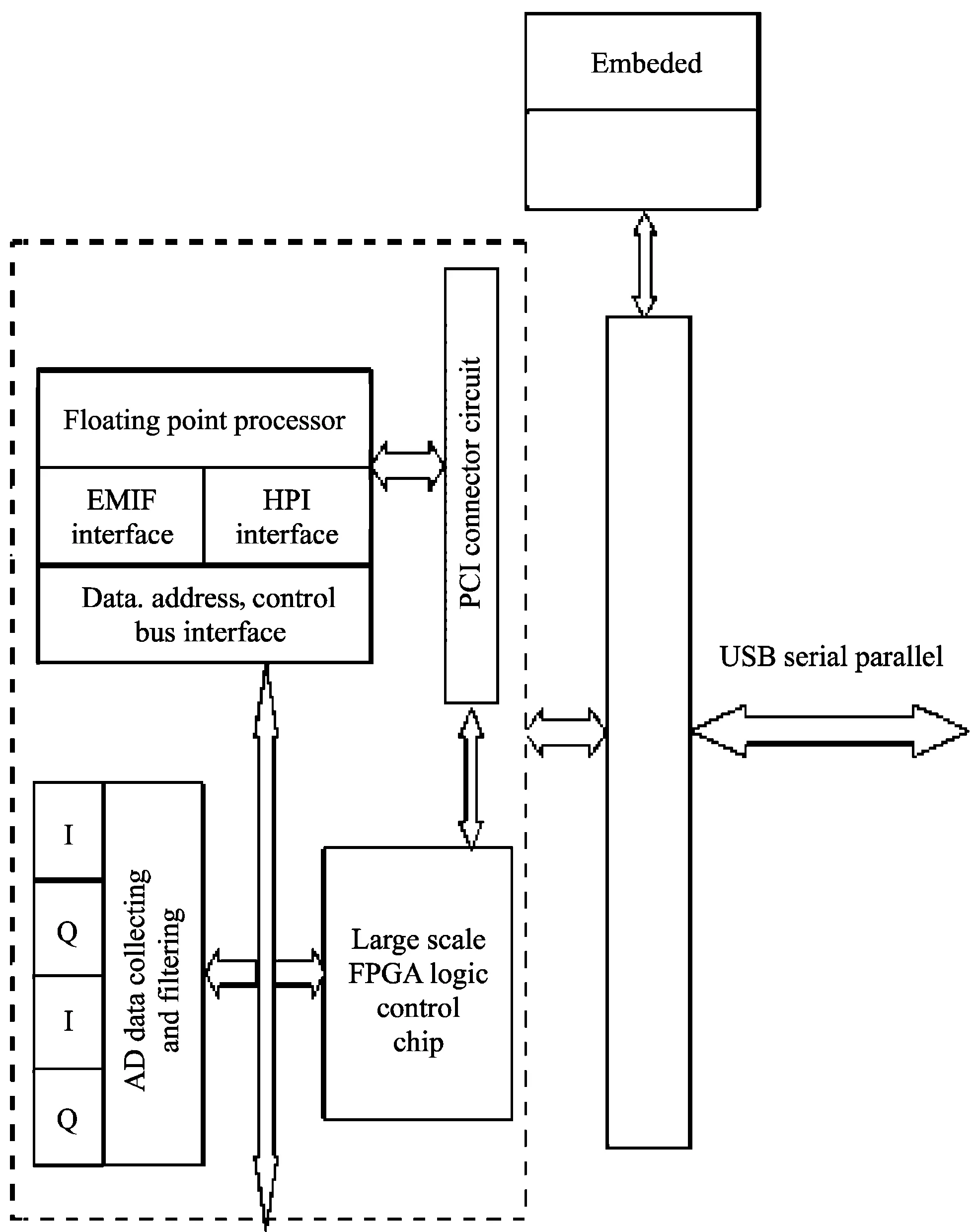
Fig.2 Connection diagram of DSP board bus
The digital IF board of the analyzer usually includes FPGA for filtering and decoding, RAMs for storing data, EEPROM for storing local board status, and IF conditioning circuits. They may also have some interfaces for communicating with the host CPU and other hardware accessing control interfaces. To enhance access flexibility and data throughput, the devices and interfaces on digital IF board can be accessed by not only DSP but also the host CPU directly via PCI interface. The analyzer system connects PCI local bus, DSP bus, host port interface bus and FPGA bus all together, thus the host can access the whole address space of DSP via the PCI interface. The devices in multi-bus systems can acquire two address spaces at the same time and each set of buses can access the whole digital IF board by means of its own address space.
The connection diagram of the digital IF board bus is shown in Fig.2.
It can be seen from Fig.2, that digital IF board bus can be accessed by host CPU and DSP simultaneously, but the two CPUs need to compete for access right to bus. FPGA acts as the bus arbitrator of the system. The arbitration mechanism is realized based on PCI bus handshaking signals: LHOLD, LHOLDA and DSP bus handshaking signals HOLD_DSP and HOLDA_DSP. It is stipulated here that the host has higher access priority and the arbitration logic programmed by VHDL is described as follows:
if(LHOLD && HOLDA_DSP && HOLD_DSP) begin HOLD_DSP=0; end
if((HOLD_DSP==0) && (HOLDA_DSP==0)) begin LHOLDA=1; end
if(LHOLD==0) begin LHOLDA=0; HOLD_DSP=1; end
DSP processor acts as the master of the digital IF board, so the other devices are all seen as peripherals of DSP. Through setting control registers of DSP: CE0, CE1, CE2 and CE3, different read-write timings and access types are acquired. For example, if CE0 space is set to 0X40, the externally connected devices will be seen as a synchronous device and DSP will synchronously read or write the device.
After the host acquires the bus control right, it can access each peripheral device of digital IF board. For example, if FPGA space is accessed only by PCI, according to PCI read-write timing, the address will be latched when address strobe signal (ADS) strobes and the data can be latched right after one clock of the ADS signal. If space is accessed by both PCI and DSP, because PCI clock and DSP clock are two independent clocks, a NAND gate or a multi-switch circuit is needed to arbitrate the access.
The host uses HPI to access DSP space. HPI has independent data line, address line (16 bit), control line, half word control line and other control lines. HPI bus can either be separated from DSP local bus or connected with each other. The connection diagram of HPI bus and FPGA is shown in Fig.3.
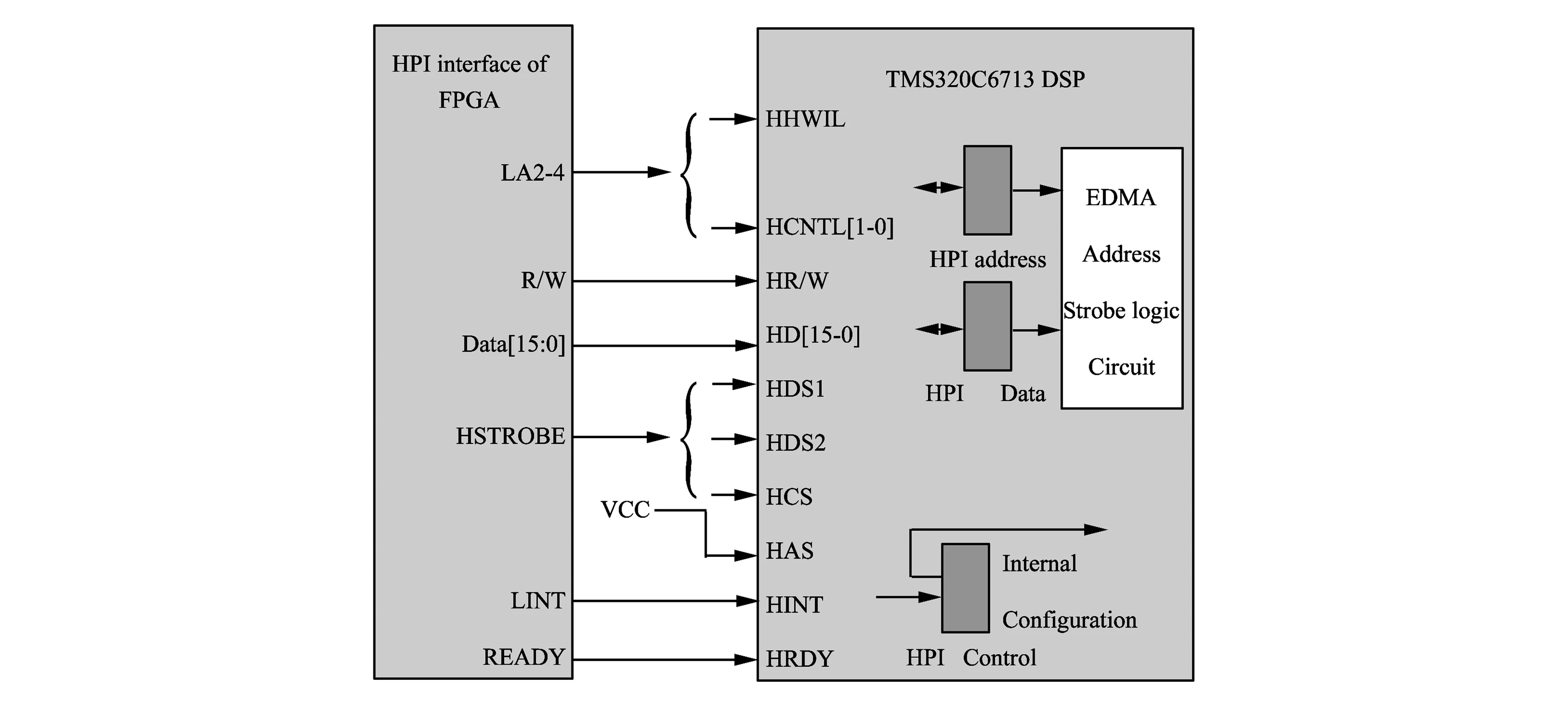
Fig.3 Connection diagram of HPI interface between FPGA and DSP
It can be seen from Fig.3 that the local bus lines LA2-4 of DSP board are used as the HPI half word address selector and HPI register addressing selector. HPI strobe signal HSTROBE is given by FPGA logic for controlling HPI address latch and read-write timing. HPI interrupt connects to PCI9054's local interrupt for sending interrupt to the host. HPI read-write finish signal HRDY is connected to FPGA, which is converted into a READY signal and then output to PCI 9054.
Fig.4 shows a typical HPI access timing initiated by the host. When PCI prompts an access of the shared bus, it will assert the LHOLD signal (LHOLD=1); If DSP is idle, PCI will get the bus and the LHOLDA signal is asserted (LHOLDA=1); FPGA logic judges the address lines to assert HCS signal, nameyly, this is a HPI access; After the address strobe signal ADS (ADS=0) and the defined data read/write time, the HRDY (HPI ready)signal is asserted, thus the READY signal is asserted (READY=0) too, which means PCI operation is done, HOLDA signal is de-asserted (HOLDA=0) and the LHOLDA signal becomes 0. The HPI operation is completed.
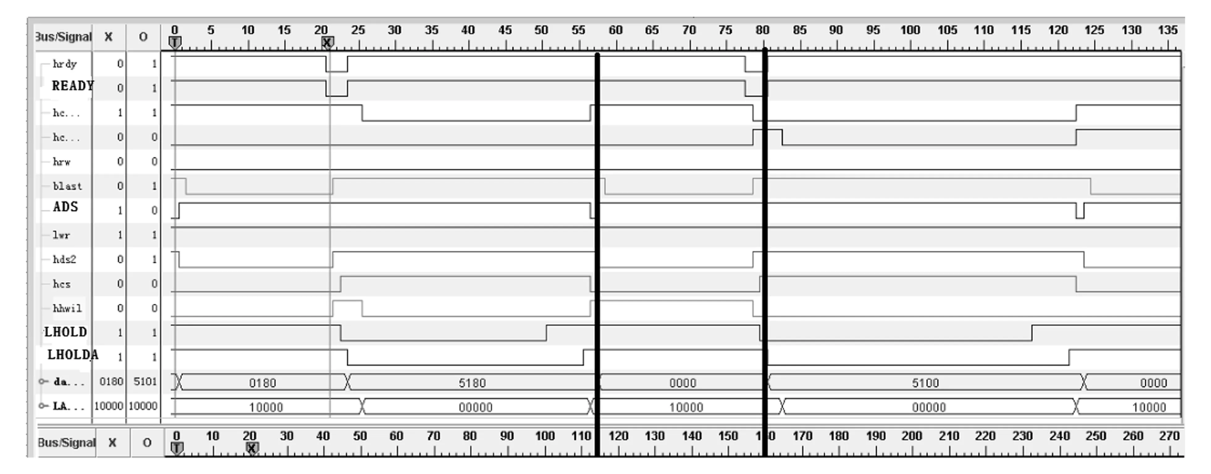
Fig.4 HPI access timing diagram
3 Conclusion
The high performance network analyzer adopts double CPU processing method, which fulfills the real-time measurement requirements, but at the same time brings difficulties to designers. Designing reasonable bus arbitration logic and reliable bus timing are the basis for the dependable operation of analyzers. The more interactions between the two CPUs happen, the more possible the bus competition will accrue. Through this shared bus design, the interactive effect between the host and DSP and the effect between external systems can decrease to the minimum owing to combined PCI bus and external bus of DSP. The data transmission between DSP processor and the host and between DSP internal RAMS and external RAMS become more effective. The various external interfaces of DSP chip can play full role and the goal of system design is achieved in the simplest and most effective way.
[1] SHEN Ping. Modern communication measurement instrument. Beijing: Posts and Telecom Press, 2007.
[2] MA Hong-lian, DING Nan, LI Yi-lu, et al. Embedded system design. Beijing: Publishing House of Electronics Industry, 2006.
[3] QU Zhao-rong. Computer software technology. Beijing: National Defense Industry Press, 2008.
[4] PLX Technology Inc. PCI 9054 data sheet. [2013-03-12]. http://datasheet.eeworld.com.cn/part/PCI9054,PLX,204754.html.
[5] Xilinx Inc. Virtex-4 data sheet. [2013-03-09]. http://en.pudn.com/downloads116/doc/detail495987_en.html.
[6] Texas Instrument Inc. TMS320C6000 peripherals reference guide. [2013-03-06]. http://www.docin.com/p-278533242.html.
[7] Texas Instrument Inc. TMS320C6000 floating point digital signal processor. [2013-03-06]. http://wenku.baidu.com/view/1b644c54ad02de80d4d84037.html.
date: 2013-08-26
LIU Dan(eiqd@ei41.com)
1674-8042(2013)04-0317-04
10.3969/j.issn.1674-8042.2013.04.003
杂志排行
Journal of Measurement Science and Instrumentation的其它文章
- A 4-layer method of developing integrated sensor systems with LabVIEW
- Calibration and compensation methods of installation error of electronic compass
- Error modeling and analysis of inclinometer based on digital accelerometer
- Analysis of condition monitoring methods for electromotor on oil platform
- U disk recorder based on CH376 and ATmega 128
- A measurement system for YTO