Review of Hybrid Packaging Methods for Power Modules*
2024-01-16,,,,
,,,,
(1.Institute of Electrical Engineering,Chinese Academy of Sciences,Beijing 100190,China;2.University of Chinese Academy of Sciences,Beijing 100049,China;3.School of Electrical Engineering,Tiangong University,Tianjin 300387,China;4.Academy for Engineering and Technology,Fudan University,Shanghai 200433,China)
Abstract: The hybrid structure of a power-module package is summarized and classified.Basic and extended planar wire-bond designs are analyzed and compared with regular wire-bond modules and planar modules,respectively.The automatic layout method can improve the electrical and thermal performance of hybrid structures.A state-of-the-art hybrid structure is introduced,and suggestions for alleviating the current and temperature imbalances for future designs are provided.
Keywords: Junction temperature monitoring,IGBT,conduction voltage
1 Introduction
With increasing demand for environmental protection and energy savings,electric vehicles (EV) have become an important means of ensuring national energy security.Almost all countries have formulated plans and achieved large-scale production in the past 10 years[1].Continuously improving product performance and reducing costs are inevitable development directions for enhancing the competitiveness of EVs[2-4].
In Ref.[5],it was estimated that approximately 80%of motor drives in EV would still use Si insulated-gate bipolar transistors (IGBTs) as power-switching devices in 2022.These power devices largely determine the performance and cost[6].In recent years,many countries have explored novel packaging methods to exploit the advantages of Si IGBT chips[7].
Packaging is a necessary process for power devices that isolates them from the external environment and protects them[8].The quality of packaging affects not only the electrical,mechanical,and thermal performance of power devices but also their cost and reliability[8-10].Additionally,power modules determine the system compactness and functions[11].
Silicon carbide (SiC) devices have emerged,which have small losses and high temperature resistance and can operate at high frequencies[12-14].They promote major technological changes in the field of EVs[15-16].SiC motor drives developed by automakers such as Tesla and BYD have been on the market for five years,demonstrating technological advantages and potential[17].
Currently,most SiC power devices use the same packaging form and specifications as traditional Si devices,with a maximum operating junction temperature of 150 ℃ or 175 ℃[18].Limited by parasitic impedance,thermal dissipation,and packaging materials,the characteristics of SiC chips cannot be fully exploited[19].The design and development of reliable packaging that satisfies high-temperature and high-frequency requirements have recently become popular research topics[20].One of the design targets is high power density.
In an EV system,for a 300-400 kW motor drive,a 1 200 V/1 500 A SiC power module that can support continuous operation at 150 ℃ is required[21-22].For a 1 500-A module,18-piece 16-mΩ SiC dies must be paralleled.For regular economy-based wire-bond packaging,it is difficult to include 36 devices in a module.As shown in Fig.1,two limitations exist[15].The first is the width of the conduction path;the minimum DBC (Direct bond copper) pattern to conduct 1 500 A is 10 mm,which is difficult to realize in a conventional wire-bond package.The second issue is thermal management,for which the balance of the paralleled devices is important[23].
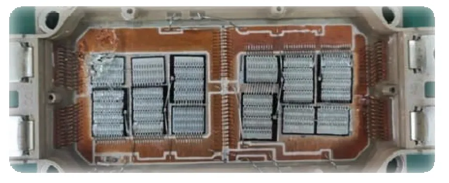
Fig.1 Econodual based wire-bond packaging[15]
A three-phase HPD module is currently preferred in the market.For a 250-300 kW motor drive,1 200 V/1 000 A operation at 150 ℃ for each phase will be very useful in the near future.As shown in Fig.2,there are many designed patterns for a 1 200 V/600 A HP drive module operating at 150 ℃[15].It is limited to eight parallel dies owing to the two aforementioned issues.
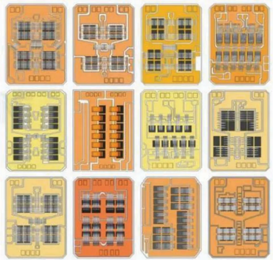
Fig.2 Conventional junction temperature estimation methods[15]

Fig.3 Planar package on semi-IDM(Integrated drive module)[24]
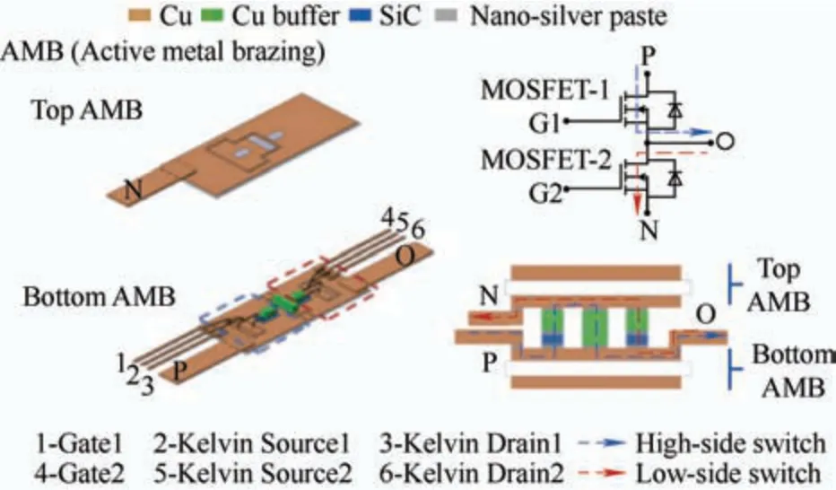
Fig.4 Planar packaged module[25]
To address this problem,researchers have begun developing planar packages[24].Typical designs are shown in Figs.3 and 4.Limited by manufacturability,cost,and feasibility,the maximum number of paralleled power devices in each product is usually 8[25].Although more than 100 papers are published annuallyon improving the quality of planar packages,there is still no systematic solution for paralleling a large number of dies.
Because the top pads of power devices have become smaller,it is difficult to control the quality of all the top interconnections.In many designs,the top connections become poor when a strong force is applied to attach the cold plate closely.This is another significant challenge in planar packaging[26].
To reduce the complexity of the planar packaging design and the fabrication procedure in Ref.[27],a hybrid packaging structure for high-temperature SiC power modules was presented[28].The structure combines the benefits of the wire-bond and planar packaging structures,as shown in Fig.5.The hybrid power module achieved almost the same footprint and parasitic resistance as the planar structure.This structure is also known as a stacked power package.
Fig.5 Concept of the hybrid structure[28]
Refs.[29-31] presented similar ideas for forming three-dimensional (3D) current commutation loops,which can reduce the parasitic inductance.In these studies,a lead frame,connection strips,and vias were used to connect the different layers.This approach does not require double-sided solderable devices.
Hybrid packaging is also a feasible and useful method for increasing the power density and paralleling numerous dies.With careful design,the parasitic parameters of a hybrid packaged power module can be significantly reduced compared with those of a regular wire-bond module[32].It can also be easily extended as the basic structure of a planar package without transfer-molded plastic,which may help build a better connection of the double-sided pin-fin baseplate.
In this study,to better exploit hybrid packages,we categorize and review the benefits and drawbacks of various hybrid structures,packaging design methods,and the applications of hybrid structures in power converters.
2 Hybrid packaging structures
2.1 Basic wire-bond-based structure
In most hybrid structures,the basic idea is to use the bottom DBC and the top conduction layer to conduct current separately.These two conduction paths usually overlap and can significantly reduce the parasitic parameters.The top conduction layers are presented in Tab.1.

Tab.1 Classification of the top-side layer
In Ref.[28],a lead frame was selected as the top conduction layer.To insulate the DBC and top layers,a high-temperature polyimide insulation material(EpoTek 600/ Duralco 128) was used to cover the conduction layers and fill the gaps.Compared with the planar structure presented in Ref.[27],this hybrid structure has the same footprint and is 50% smaller than the baseline wire-bond version.However,the fabrication procedure is complex,as shown in Fig.6.
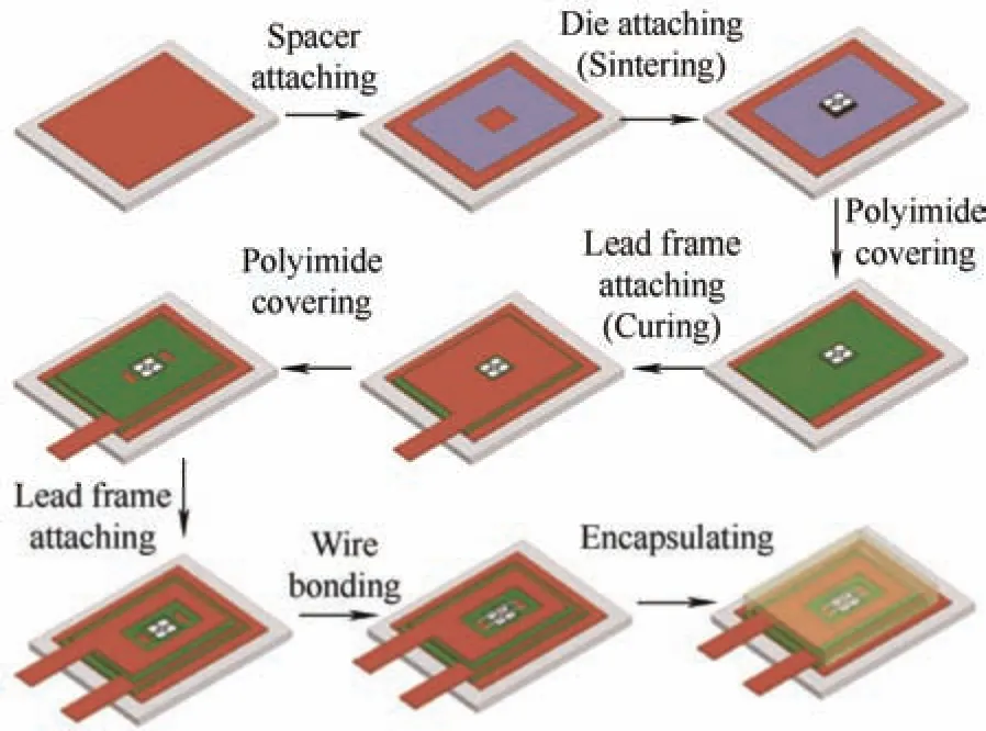
Fig.6 Complex fabrication procedure[28]
To reduce the complexity,a multilayer printed circuit board (PCB) with vias was used as the top conduction layer in Ref.[30].In addition to a simpler structure,more complex routing can be achieved using PCBs.This allows current paths to be more flexible and allows an embedded gate-driver circuit to be embedded in the module.As shown in Fig.7,a small footprint was achieved,compared with that of a regular TO-247 discreet device.
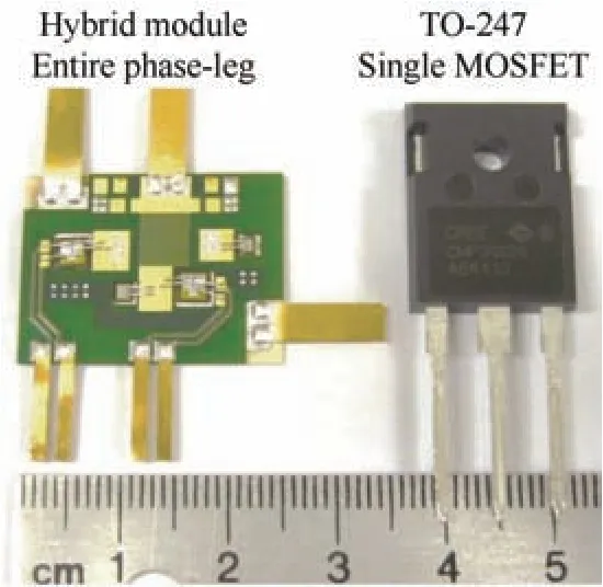
Fig.7 PCB used as the top layer[30]
However,unless a special high-temperature insulation layer is used in the PCB,it is difficult to directly bond the DBC and top layers using a regular reflow procedure.Additionally,a large current (>300 A) may not be easily achieved by the thin copper layer of a regular PCB.
By using a flexible PCB as the top layer[31,36],an inductance of <1 nH was obtained in the power loop.Simultaneously,the gate drive,decoupling capacitors,and DC-link capacitors were integrated with flexible PCBs,as shown in Fig.8.Vias were used to transfer the current from the top layers to the DBCs.In contrast,flexible PCBs were bent and directly soldered onto the DBC in Ref.[32].The parasitic inductances in the power and gate loops decreased by 52% and 76%,respectively.
In Ref.[37],DBC was used as the top conduction layer,and a low stray inductance and balanced current sharing were achieved.As shown in Fig.9,two layouts with the power terminals in different locations can both support the paralleling of five SiC dies.However,it is difficult to parallelize more dies with these designs.
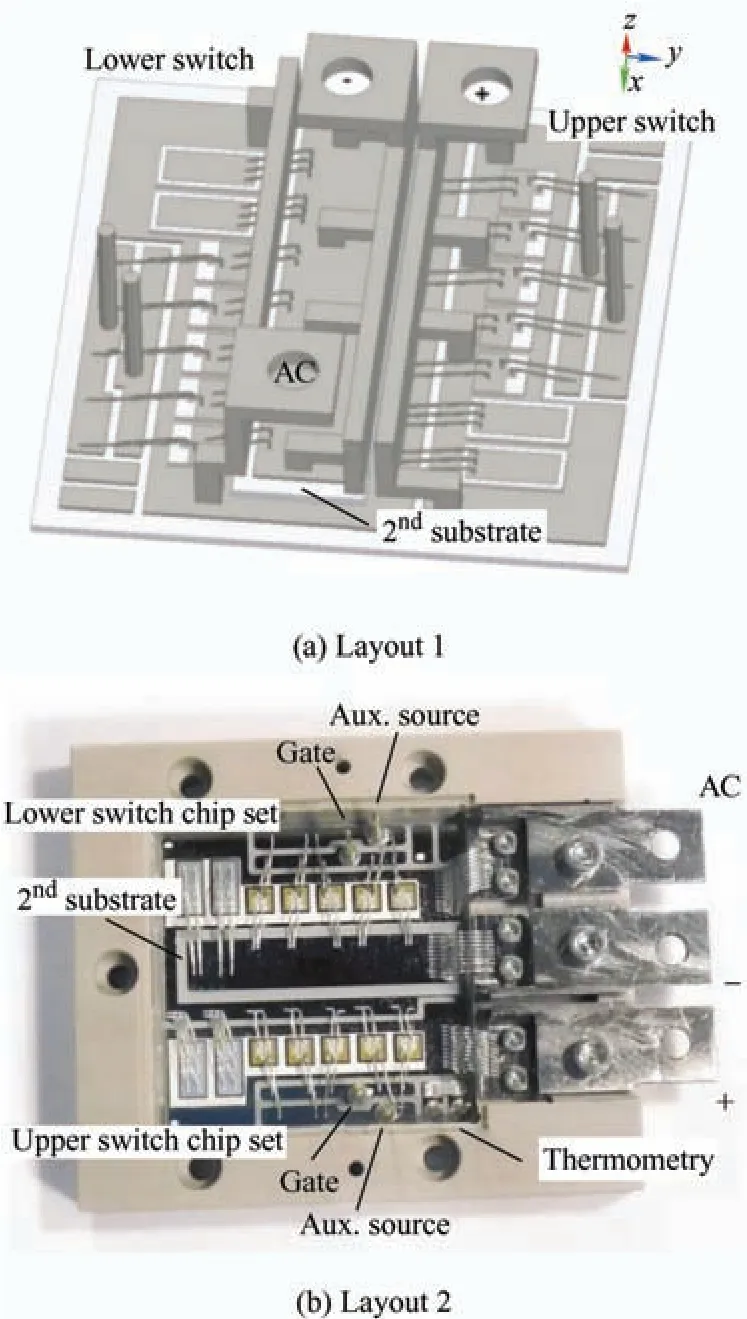
Fig.9 ABB hybrid structure using DBC as the top layer[33]
To realize a high-current power module[36],a method that separates the module into four individual units is presented.This can increase the manufacturing yield in mass production.Additionally,the power and gate paths can be better balanced with a symmetric design.With this structure,18 dies can be paralleled in a phase-leg design with an economically sized power module,as shown in Fig.10.With a similar idea,a power module with nine paralleled 25-mΩ dies was designed and fabricated in Ref.[38].A 800 V/900 A double-pulse test at 150 ℃ was conducted.

Fig.10 Stacked module design with 18 paralleled dies[32]
2.2 Planar top interconnection-based structure
As reported in Ref.[39],double-sided cooled power modules have several advantages over single-sided cooled modules.Most planar power modules can achieve a lower parasitic inductance and higher packaging density.The thermal performance can be improved by double-sided cooling;thus,temperature swings and thermal stress may be reduced.Theoretically,eliminating wire bonds in planar packages can extend their lifetimes[40].
Hybrid structures can be easily changed to planar packaging if the wire bonds are replaced with copper strips or DBCs.Tab.2 classifies the main planar structures by the top-side connection style and introduces an extended hybrid structure.With three or four conduction layers in the power module,the extended hybrid structure has a more flexible design than common planar packages.
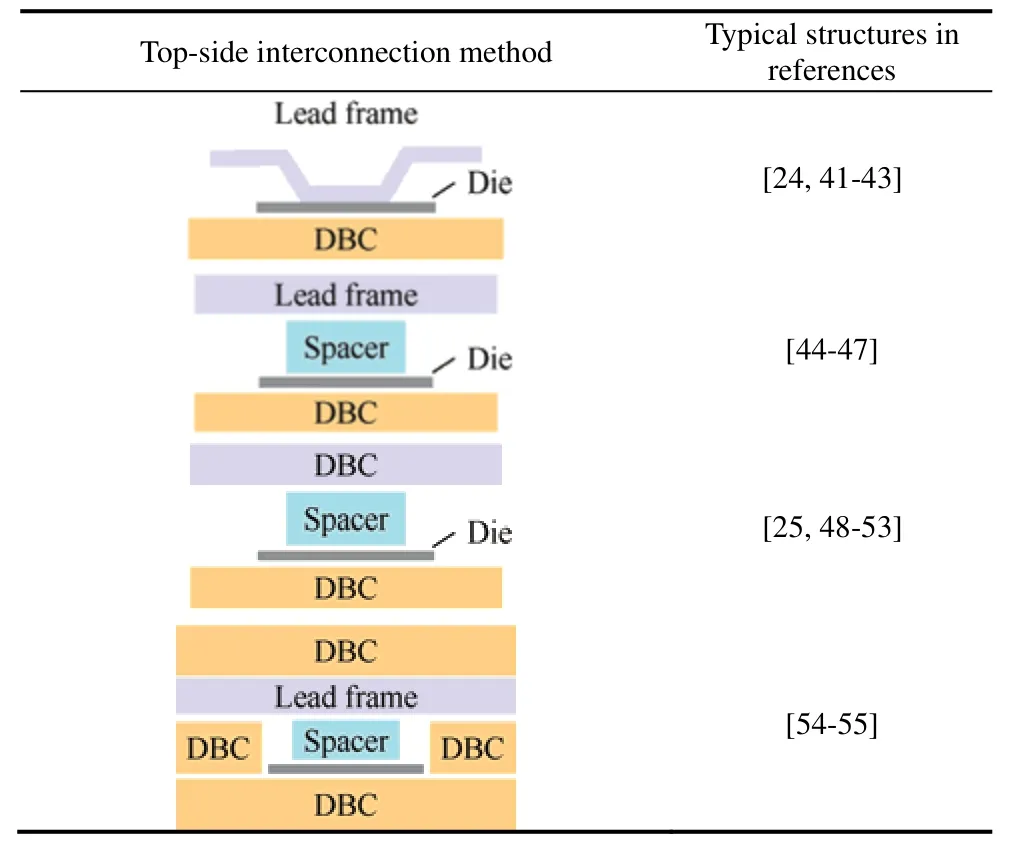
Tab.2 Top-side interconnection method
Another benefit of the extended hybrid structure is its large support area.As shown in Fig.11,in the typical planar structures,other than transformed plastic,dies are the only effective support.In Ref.[40],the total area of the dies was approximately 1/4-2/5 of the total power module.Thus,dies may be overstressed if the pressure is not well controlled during the bolting to the cold plate[41].Transfer-molded plastic is the only choice for reducing stress on dies,particularly in commercial products[45,56].With transfer-molded plastic,it is relatively difficult to solder the heat sink directly in the packaging procedure[57-58].Thermal grease must be applied on both sides of the DBC,which may significantly increase the thermal resistance[59].In the extended hybrid structure,a second layer of DBC surrounds the die[60].It can provide additional support for the top DBC and even the top pin-fin baseplate[55,61].Because the area of the second-layer DBC is usually approximately two to four times the die area,the stress is significantly reduced.With this support,the extended hybrid can omit the transfer-molded plastic and only use a regular encapsulant,as in the wire-bond module.Thus,the manufacturability can be improved,and a double-sided pin-fin plate can be easily soldered.
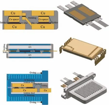
Fig.11 Typical planar structures[40]
In some planar methods,the researchers soldered the phase-leg dies on the top and bottom conduction layers separately and then flipped the top layer side,as shown in Fig.12[49,62].Subsequently,they were stacked into full pieces.However,it is difficult to control the flatness of both soldering sides,and paralleling a large number of dies is almost impossible[40].Thus,large-scale manufacturing is difficult.

Fig.12 Flipped DBC method in planar packages
In other methods,to simplify the fabrication procedure and control quality,power dies are soldered only on the bottom conduction layers[63].This implies that the midpoint should exist in both the top and bottom conduction layers[64].There must be a transfer interconnection point in the package,and the main methods for this current transfer are presented in Tab.3.An extended hybrid structure was obtained using this final method.
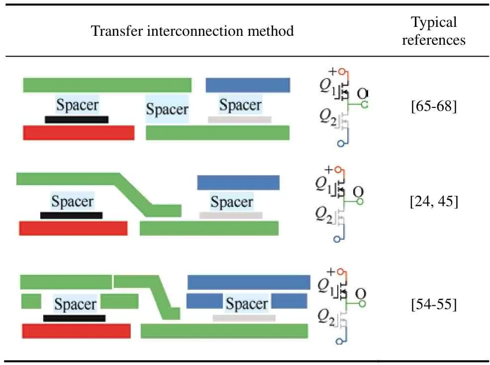
Tab.3 Transfer interconnection methods
To achieve a high-current power module,Ref.[55]presented a method that separates packages into individual units to improve manufacturability.With this structure,12 dies can be paralleled for each phase leg in a compact power module,as shown in Fig.13.In Fig.13,1 is DC positive terminal,2 is DC negative terminal,3 is AC terminal,4 is DBC on the lower part of the upper tube,5 is DBC on the lower part of the upper tube,6 is SiC chip on the upper tube,7 is SiC chip on the upper tube,molybdenum chip on the upper tube,8 is copper chip on the upper tube,9 is copper chip on the upper and lower bridge,10 is DBC on the lower part of the lower tube,and 11 is DBC on the lower part of the lower tube.12 is lower tube SiC chip,13 is lower tube SiC chip connected to molybdenum sheet,14 is lower tube connected to copper sheet.In Ref.[54],a double-pulse test at 800 V/400 A at 150 ℃ was conducted on a power module with the same structure.
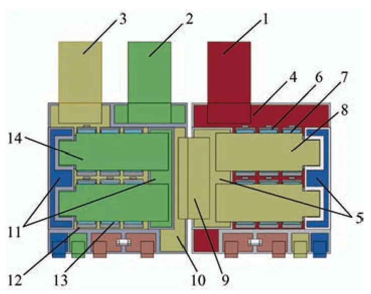
Fig.13 Layout of the stacked planar power module[55]
3 Hybrid module design considerations
3.1 Electrical design for hybrid module
In Ref.[30],the power module had a single MOSFET and a diode in each switch of the phase leg.Kelvin connections were used to isolate the main and gate currents of the MOSFETs.The MOSFETs and diodes were paired to minimize the switching loops.To further reduce the parasitic parameters,ceramic DC decoupling capacitors were integrated into the module,as shown in Fig.14.Compared with the conventional wire-bond module,the loop inductance was reduced by 35%,and the footprint was reduced by 40%.The loop inductance was measured as 3.6 nH,which agreed well with the simulation.

Fig.14 Paired MOSFETs and diodes[30]
Ref.[25] proposed a hybrid package consisting of two DBC substrates,SiC devices,bonding wires,power terminals,and signal terminals.As shown in Tab.2,the structure had a short power loop with mutual inductance cancellation,and it exhibited an ultralow parasitic inductance.
In Ref.[31],the bonding wires were oriented toward the power terminals to shorten the loop.The smallest commutation-loop area was achieved by comparing several possible electrical designs,as shown in Fig.15.Through Ansys Q3D simulations,the parasitic parameters were extracted and compared.The optimized parasitic inductance was only 1.8 nH.Ref.[36] also reported test results.The voltage overshoot was reduced by 55% compared with that of a commercial power module,and the total switching energy was reduced by 57% (Fig.16).

Fig.15 Paired MOSFETs and diodes[31]

Fig.16 Layout comparison[36]
Ref.[34] reported similar results.In a finite-element analysis (FEA) simulation,the gate path inductance and power path inductance were reduced by approximately 76% and 50%,respectively.As shown in Fig.17,both the ringing and the power loss were reduced.
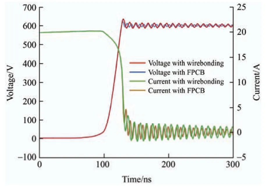
Fig.17 Waveform comparison[34]
Ref.[38] introduced a stacked power module with nine power dies paralleled,as shown in Fig.18.Compared with the conventional wire-bond module,the novel structure exhibited a neat waveform.

Fig.18 Power module with nine dies paralleled and a neat waveform[38]
3.2 Thermal design for hybrid module
The design and evaluation of the cooling capability are core steps in packaging development[69].In most studies,the thermal network models have been abstracted.As shown in Fig.19,in Ref.[31],a low thermal resistance of 0.225 ℃/W was obtained.A reduction of approximately 40% was reported compared with the traditional method(baseplate+TIM(Thermal interface material)+heatsink).
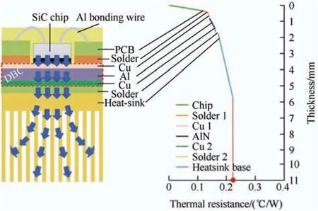
Fig.19 Thermal-resistance calculation in Ref.[31]
To improve the reliability of the power module and reduce the junction temperature variation,a thermal buffer layer was added to the power module[70].Extra heat was absorbed by the buffer layer,and the temperature fluctuations were reduced.Phase-change materials was used as the buffer layer and placed around the SiC MOSFETs,as shown in Fig.20.This technology can also be applied to hybrid structures.
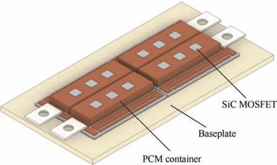
Fig.20 Improved thermal dissipation method[70]
Through computational fluid dynamics (CFD)simulations,the airflow condition and temperature distribution of the converter system can be analyzed.In Ref.[31],the suction-mode fan and exhaust-mode fan were compared,and the distribution and centralization fan configurations were analyzed.The temperature increase in the magnetic cores and dies was carefully considered to ensure safe and high-power-density operation,as shown in Fig.21.

Fig.21 Thermal-performance simulation presented in Ref.[31]
In Ref.[37],using a flexible PCB,the power module was separated into three submodules.They were mounted on three sides of the heat sink.Accordingly,as shown in Fig.22,a 3D system-in-package integration method was proposed,and the volume of the forced air cooling system was only 0.346 L.

Fig.22 3D system-in-package integration and thermal simulation[37]
In EV applications,water cooling is the optimal cooling method for most motor drive systems.Pin fins are commonly used in wire-bond power modules.A thinner pin exhibits a smaller pressure drop,which typically corresponds to a higher flow speed.Each layout design has an optimal fitness.It is difficult to directly compare with analytical equations,because convection cooling involves turbulent flow.As shown in Fig.23,CFD-based simulations have been widely used in several commercial module designs[15].
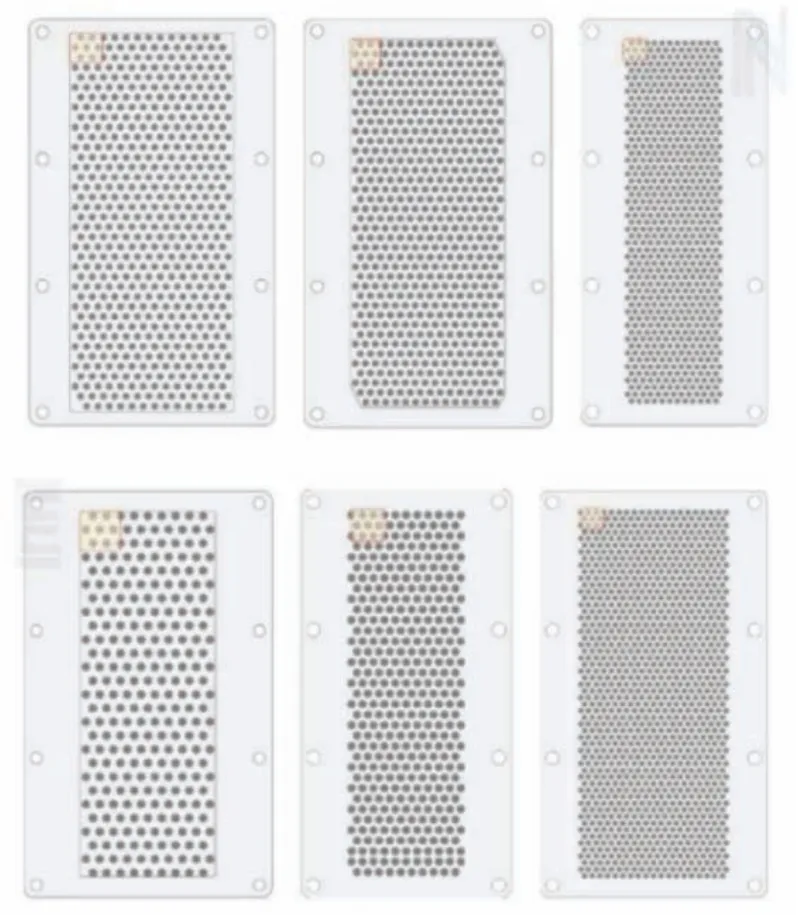
Fig.23 Pin-fin optimization[15]
However,when coolant flows through the pin fins,there must be parallel,serial,and/or mixed flows[71].For minimizing the temperature difference between the dies,the pin-fin designs close to the inlet and outlet areas should not be identical.Manually comparing hundreds of layout designs using CFD is difficult.Thus,automatic layout optimization of the power module should be used to achieve the optimal electrical and thermal designs[72].
3.3 Automatic module optimization method
To fully explore the fast switching capability of advanced power devices,low parasitic parameters are crucial[73-74].Ref.[75] provides an example of layout optimization.As shown in Fig.24,a lead-frame-based planar module was fully considered and designed with a power-loop layout.Compared with state-of-the-art power modules,several additional features were integrated into the proposed module,with a similar power rating and volume.
Fig.24 Experience-based layout design[75]
However,for most manual designs,the number of design candidates was less than 30.Researchers have attempted to find better solutions and explore automatic layout design methods[76].These automatic designs have already achieved crucial cost savings in power module design.They can automatically perform advanced model abstractions,electrical parasitic extractions,and thermal analyses[77].As shown in Tab.4,in automatic design,the first step is the automatic generation of design candidates,which typically include component representations,placement methods,and routing methods.
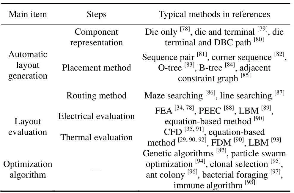
Tab.4 Typical automatic design items
Similar to regular wire-bond modules,the shortest and most feasible wire bonds are commonly used in hybrid structures.Detailed wire-bond connections do not require special descriptions in the code.Thus,the optimization procedure can be accelerated by coding only power devices and terminals in the string[82].
Almost all the placement methods in automatic design can be easily extended to hybrid structures by simply repeating the coding procedure at the top layer.The routing methods for a regular planar module can be directly applied to a hybrid structure.Additionally,almost all optimization methods can be used in hybrid packaged modules.
In the electrical performance evaluation step,the finite-element method can achieve the highest accuracy;however,the geometry must be redrawn and re-meshing must be performed for each candidate[31].This method is too slow for automatic layout optimization.In comparison,the partial element equivalent circuit (PEEC) can significantly reduce the simulation time but slightly increases the error,as shown in Tab.5[99](Rank from 1 to 4;1 is the best,and 4 is the worst).
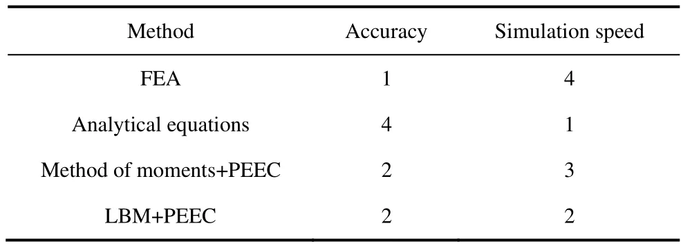
Tab.5 Electrical evaluation methods
During the routing procedure,an incorrect connection may occur during the path autogeneration step.In the electrical evaluation step,the judgement of the correctness of all connections accounts for a large portion of the evaluation time.To accelerate the judgement,a lattice Boltzmann method (LBM)-based method was proposed in Ref.[89].Because the LBM does not need to solve matrices directly,it can make a judgement in the middle of the calculation.This reduces the total electrical evaluation time by up to 40%.Moreover,with a larger number of components,the computational advantage of the LBM is more significant.
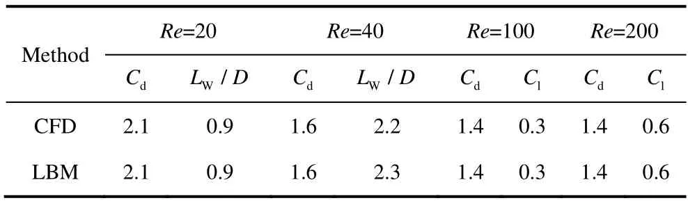
As shown in Tab.6(Rank from 1 to 4;1 is the best,and 4 is the worst),the most accurate simulation method for evaluating the thermal performance of a power module with a pin-fin baseplate is the finite element analysis (FEA).This is a conventional CFD method[100].However,it takes a long time to evaluate the candidates and is difficult to embed in the optimization loop because of meshing and convergence issues.In contrast,analytical equation-based methods are fast,but the relative error may exceed 30%[92].

Tab.6 Thermal evaluation methods
In Refs.[101-102],improved finite difference methods (FDMs) were used to solve the partial differential equations of Stokes’ theorem.They can balance accuracy and simulation speed.Moreover,these methods can be easily used in iterative optimization.The LBM is a special type of FDM for solving partial differential equations.It is believed that the LBM is faster than the other FDMs because it has an innate parallel calculation ability.With the help of the turbulence model,the LBM can be used to simulate the inlet and outlet pressure differences and the flow velocity around the cylinders of the pin-fin heat sink power module.Owing to its easy coding features,it can be integrated into optimization algorithms.
Ref.[93] presented a power module optimization demonstration and achieved good performance.A simulation with the LBM had a smaller error than a simulation based on CFD,as shown in Fig.25 and Tab.7.
Tab.7 Literature comparison[93]
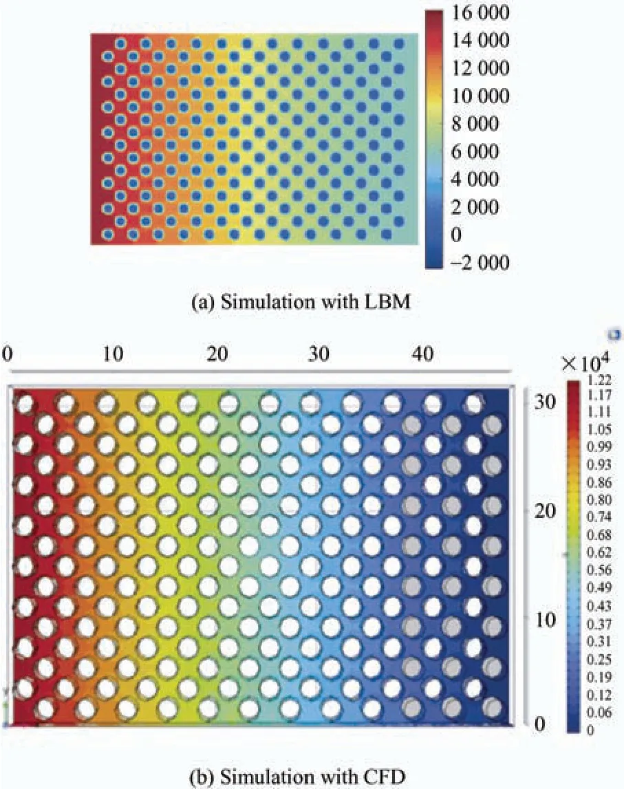
Fig.25 Thermal evaluation comparison[93]
4 Hybrid modules in power converters
To demonstrate the small footprint and parasitic parameters of the hybrid-structure packaging,a three-phase single-switch rectifier was used as an example[28].To simplify the control,the circuit uses seven SiC diodes and one SiC power switch,as shown in Fig.26.Through a detailed simulation and comparison,the footprint of the hybrid structure was found to be equal to that of the planar structure and 50% smaller than that of the regular wire-bond structure.In the system simulation,the voltage spike of the power switch was reduced from 305 V to 289 V compared with the wire-bond version,indicating a significant parasitic reduction in the power path.A high-temperature converter test was successfully conducted to verify the packaging design.In the test,the junction temperature was maintained at 250 ℃,and the total converter efficiency reached 96.1%.
In Ref.[36],a hybrid module-based converter system was operated in a 100-kHz hard-switching mode,and it achieved a peak efficiency of 98.3%.The electrical design and thermal design are presented in detail in Fig.27.The difference in efficiency between the design and experiment was <1%,and the difference in temperature was <8 ℃.Parasitic inductance reduction and thermal resistance reduction were achieved,and a systematic design procedure for the hybrid structure was demonstrated.
Fig.27 Hybrid package used for a high-switching-speed converter[36]
In Ref.[37],for a hybrid-module-based three-phase converter,a 20-kW forced air cooled system was designed,as shown in Fig.28.Power tests verified a peak power density of 19.3 kW/L.The experimental results also indicated a far smaller voltage overshoot,1.8 times faster switching,and 60% switching loss reduction compared with the regular wire-bond module.

Fig.28 Hybrid package used for a three-phase converter[37]
With the submodule using hybrid packages,Fig.29 shows the interleave ability for a 5.5-kW water-cooled single-phase inverter[35].Compared with the commercial wire-bond module,the inverter loss was reduced by 16.1% at a switching frequency of 20 kHz and 28% at a switching frequency of 120 kHz (Fig.29).This implies that with the same efficiency,the switching frequency can be increased to 1.7 times that of the regular module.

Fig.29 Hybrid package used for a interleaved single phase converter[35]
In summary,hybrid packaged module-based converters have considerable potential for increasing the power density.They can exploit the advantages of power devices and achieve high efficiencies.
5 Conclusions
To better exploit the advantages of the hybrid power packaging structure,the basic structure,extended planar structure,electrical design,thermal design,automatic layout methods,and related converter system designs are reviewed.Through comprehensive classification and comparison,the hybrid structures were introduced and discussed.The presented hybrid structures are summarized in Tab.8.
Tab.8 Summary and comparison of hybrid structures
The following conclusions are drawn.
(1) The hybrid structure can significantly reduce the parasitic parameters and can be used to parallelize a large number of dies.
(2) The extended planar package based on the hybrid structure exhibited more 3D interconnection freedom.An advanced layout can be designed using this feature.Because DBCs are used to support the stress,the structure can eliminate transfer-molded plastic.
(3) Thermal design is important,as the power density can be increased by >30% compared with that of a regular wire-bond module.Automatic layout and thermal optimization methods should be improved and utilized in future designs.
In the near future,to further exploit the advantages of the hybrid package,four points should be noted.First,to reduce the parasitic parameters and balance the parallel devices in the gate path,the positions of the gate terminals can be designed in the center layout of the power module.Second,when the current rating is increased,the transfer interconnection should be carefully designed.Third,for power modules operating at >1 000 A,the use of multiple power terminals at the same electrical point should be considered to increase reliability.Finally,because hybrid structures may increase the number of packaging steps,the manufacturing capability and cost should be considered for production.
Hybrid-structure packages allow the deep exploration of power devices and can increase the capacities of power modules.
杂志排行
Chinese Journal of Electrical Engineering的其它文章
- A Review of Isolated Bidirectional DC-DC Converters for Data Centers*
- Vibration Reduction and Torque Improvement of Integral-slot SPM Machines Using PM Harmonic Injection*
- Calculation of Available Transfer Capability Using Hybrid Chaotic Selfish Herd Optimizer and 24 Hours RES-thermal Scheduling
- Filtered High Gain Observer for an Electric Vehicle’s Electro-hydraulic Brake: Design and Optimization Using Multivariable Newton-based Extremum Seeking
- Improved Approaches Toward Analysis of Electromagnetic Processes in Electrodynamical Devices Based on the Theory of Electromagnetic Field
- A Novel Modified Fuzzy-predictive Control of Permanent Magnet Synchronous Generator Based Wind Energy Conversion System