A Hybrid Five-Level Single-Phase Rectifier with Low Common-Mode Voltage
2024-01-12TIANRuihanWUXuezhiXUWenzhengZUOZhilingCHENChangqing
TIAN Ruihan, WU Xuezhi, XU Wenzheng,ZUO Zhiling, CHEN Changqing
(1. Beijing Jiaotong University, Beijing 100044, China;2. ZTE Corporation, Shenzhen 518057, China)
Abstract: Rectifiers with high efficiency and high power density are crucial to the stable and efficient power supply of 5G communication base stations, which deserves in-depth investigation. In general, there are two key problems to be addressed: supporting both alternating current (AC) and direct current (DC) input, and minimizing the common-mode voltage as well as leakage current for safety reasons. In this paper,a hybrid five-level single-phase rectifier is proposed. A five-level topology is adopted in the upper arm, and a half-bridge diode topology is adopted in the lower arm. A dual closed-loop control strategy and a flying capacitor voltage regulation method are designed accordingly so that the compatibility of both AC and DC input is realized with low common voltage and small passive devices. Simulation and experimental results demonstrate the effectiveness and performance of the proposed rectifier.
Keywords: multilevel rectifier; 5L-ANPC; low common-mode voltage; AC-DC hybrid input
1 Introduction
With the development of 5G networks, reliable power supply is the key to ensuring the safe and stable operation of communication systems.Higher power efficiency, lower power noise, and higher stability and reliability are required. Therefore, the application of power factor correction (PFC) rectifiers in communication power supply has attracted wide attention[1-3], mainly to meet the power quality requirements of 5G communication base stations as well as the need for alternating current (AC)and direct current (DC) input switching[4].
At present, many researchers study multilevel converters[5-6], which can control the output terminals of different DC power supplies connected in series through a specific circuit topology. With the change of different switching states of the circuit, the multi-step wave can be equivalent to a sine wave.Compared with the traditional two-level converter, multilevel converters have the following advantages: 1) The voltage stress of semiconductor switching devices is reduced to achieve a higher level of voltage and power output; 2) it has high output power quality, smaller dv/dt, low total harmonic distortion(THD) and electromagnetic interference; 3) it can operate at both the fundamental wave and high frequency switching frequency, reducing the switching loss of power switches and improving system efficiency. Thanks to the above advantages,multilevel rectifiers are widely used in power supply systems, power factor correction, battery energy storage systems and other applications[7-8]. However, the multilevel converter still has some shortcomings, one of which is that the number of switching devices increases exponentially with the increase of the level numbers, and each switch requires a gate driving circuit, which complicates the control strategy of the system and increases the cost[9]. In order to pursue better performance, researchers continue to innovate and improve the multilevel topology.
Among various multilevel converters, the five-level active neutral-point-clamped (5L-ANPC) topology is a topology with high practicability and good economy. Compared with the cascaded H-bridge (CHB) converter, only one DC source is needed. Compared with the neutral-point-clamped (NPC) converter, the number of clamping devices is reduced. Nevertheless, the number of redundant switches is increased by introducing the flying capacitor. The DC link is divided into two parts, which reduces the difficulty of voltage equalization of the DC capacitor and realizes the capacitor voltage balance through a certain control algorithm. Compared with the flyingcapacitor (FC) converter, 5L-ANPC greatly reduces the amount of capacitance used and has great advantages[10]. In order to suppress the common-mode voltage better, the combination of upper and lower bridge arms is adopted to further increase the number of levels and reduce dv/dtin this paper.Otherwise, if the 5L-ANPC topology is adopted for both upper and lower bridge arms, 16 switches are required. The number of switches is too large to meet the requirements of high power density. This paper presents a hybrid rectifier topology by combining the upper bridge arm 5L-ANPC and lower bridge arm diodes.
The rest of the paper is organized as follows. In Section 2,the operating characteristics and the control strategy of the 5LANPC hybrid rectifier are introduced, including FC voltage regulation. In Section 3, simulations and experiments verify the effectiveness and performance of the strategy proposed in Section 2. Finally, the conclusion is given in Section 4.
2 Working Principle
2.1 Topology Analysis
A traditional multilevel topology is difficult to apply in five or higher levels because of the inability to control the point voltage in the bus bar and the excessive number of clamping elements. The 5L-ANPC has aroused wide concern after it was proposed. It can improve the output voltage level, using fewer devices when outputting the same number of levels, and its capacitor voltage equalizing control algorithm is relatively simple, which has great application potential in switching power supply.
The AC/DC rectifier circuit needs to realize power factor correction and suppress common-mode current. More levels can be achieved through the combination of upper and lower bridge arms, but it conflicts with the demand for high power density. Therefore, the topological structure of five levels on the upper arm and the diode on the lower arm is adopted, as shown in Fig. 1.

▲Figure 1. Topology of hybrid 5L single-phase rectifier (adopting twostage bridge scheme)
The upper bridge arm is a single-phase 5L ANPC converter topology, consisting of 8 switches with inverse shunt diodes,an FCCf ,and two supporting capacitorsC1andC2on the DC side. The first part consists of two supporting capacitors and four switching devices, which are used to clamp the busbar voltage. The latter part uses the FC structure for multilevel output. Assuming that the voltage at the DC side is 4E, the conditions for the topology to work properly are as follows. 1)The voltage of the two support capacitors at the DC side is basically the same, that is,UC1=UC2=Udc/2 = 2E.2) The voltage of the flying span capacitor is ensured to be basically stable, i.e.,UCf=Udc/4 =E.
The corresponding switching devices of 5L ANPC converter topology are complementary, and their actions must follow the following switching principles[8]: 1) The switching devicesS1andS3,S2andS4must be turned on or off at the same time,respectively. The two groups are complementary and operate at power frequency; 2) The switching devicesS5andS7,S6andS8should be complementary respectively and operate at the switching frequency; 3) When switching mode of switches is selected, two pairs of switch devices operating at the same time is usually avoided.
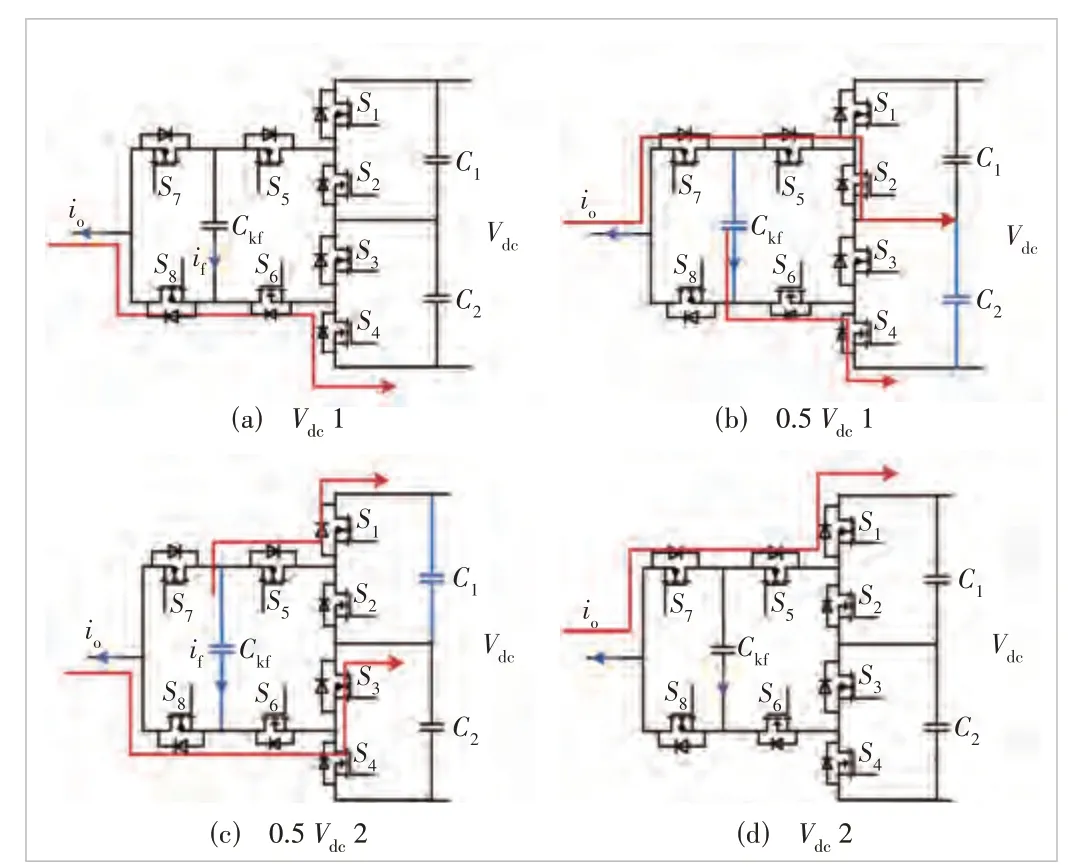
▲Figure 2. Status of the direct current (DC) input switching
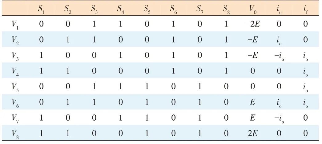
▼Table 1. Five-level active neutral-point-clamped (5-L ANPC) converter switching
The positive direction of the output currentioof the converter bridge arm and the FC currentifare denoted in Fig. 2.All switching states and their related currents can be obtained in Table 1. It can be seen that there are eight different switching states fromV1toV8, and the rectifier can produce five voltage levels under the equilibrium condition, namely 0.5Vdc,0.25Vdc, 0, -0.25Vdcand -0.5Vdc. When the output level is-E, 0 andE, there are two redundant switching states respectively, and when the output level is -EandE, the corresponding two switching states, namely (V2,V3) and (V6,V7), have opposite effects on the charging and discharging of the FC voltage. The voltage equalizing control of FC can be realized by adjusting the two switching states properly.
For a single-phase rectifier, common-mode voltage is defined asVcm=(Va+Vb)/2, whereVa, andVbare the voltages of bridge armsAandB, and the common-mode current has a direct relationship with the amplitude of common-mode voltage and the step slope dVcm/dt. Therefore, effectively reducing the amplitude and jump slope of common-mode voltage can effectively reduce the common-mode current.
The proposed five-level topology has a total of eight switching devices, which need to provide eight +15 V/-5 V on/off signals to ensure the safety and accuracy of the driving signals. The vertical switchesS1-S4are operated at the power frequency and can be isolated from the main circuit by an isolation transformer. The switchesS5-S8are operated at the high frequency, where the upper and lower pairs are conducted complementarily. To simplify the drive circuit and reduce the cost and complexity of hardware implementation, the bootstrap drive circuit can be adopted to split the power supply into two groups to reduce the number of independent isolated power supplies.
2.2 DC Input Case
The proposed converter also supports DC input voltage. For the DC input case, the operation of this converter is downgraded to a three-level boost circuit. In order to preserve the five-level scheme under AC input and avoid the problem of large common mode inductance required by the two-level scheme for DC, the three-level control strategy for DC is adopted after research.
In the proposed three-level control strategy,VCkfshall be equal to (1/2)Vdc, namely 200 V. Voltage levels 0, 0.5Vdc,andVdcare used to synthesize voltage. When duty cycled<0.5, 0 and 0.5Vdcare used to synthesize voltage; when 0.5<d<1, 0.5VdcandVdcare used to synthesize voltage. There are four switching states as shown in Fig. 2, among which 0.5Vdccorresponds to two switching states. The FC is used to realize time-sharing in parallel with the upper and lower capacitors, so as to achieve voltage balancing between capacitorsC1andC2. The on-off time of the two switching states is the same and the carrier phase-shift modulation strategy, phase-shift pulse width modulation (PS-PWM), is adopted. For the DC input case, the three-level switching states are shown in Table 2.
2.3 Control Strategy
Regarding the design of a single-phase five-level rectifierwith excellent performance, it is necessary to meet the following aspects: achieving unit power factor operation and ensuring that the output voltage of the DC side is stable within an allowable error range. Therefore, a double closed-loop control method is proposed for the 5L ANPC rectifier studied. The AC input control block diagram of the circuit topology is shown in Fig. 3.

▼Table 2. 3-L boost switching table in a direct current (DC) case
1) Dual control loops: The dual closed-loop control strategy of the voltage outer loop and current inner loop is adopted.The outer loop voltage control mainly tracks the DC side voltage magnitude to realize voltage stability, so as to reduce the DC side voltage fluctuation as much as possible. By taking the difference between the DC side voltage sampled in real time and the reference voltage, the difference is processed and fed back to the system by the voltage regulator to control the DC voltage of the bus side. The current control target of the inner loop is the current magnitude of the filter inductor on the AC side. Compared with the given signal of the inner current loop obtained after the setting of the outer voltage loop, the power factor can be adjusted to keep the current sinusoidal. The signal processed by the current controller is used as the modulated signal of the main circuit switching device, which is compared with the triangular carrier to generate a PWM wave.
The switching function of the switchesS1andS3is defined asSf13, the switching function of switchesS5andS7is respectivelySf5andSf7, and then the output voltage can be written as:
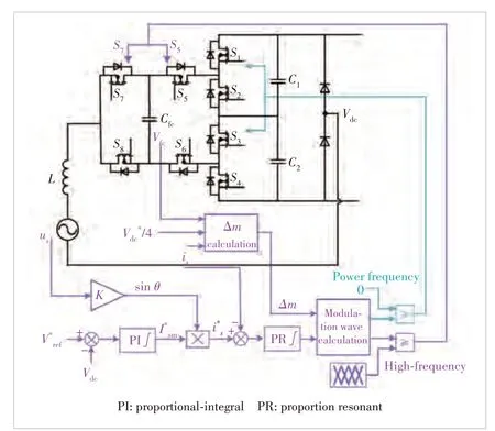
▲Figure 3. Feedforward control block diagram
2Eis selected as the voltage base value, and then the standardized output voltage range is [-1, 1]. To make the switchesS1andS3work at the fundamental frequency,Sf13can be written as:
wherevois the reference value of the single-phase input voltage. Phase-shift pulse width modulation (PSPWM) is adopted in this paper with superior ability of FC voltage control. According to the principle of PSPWM modulation, the modulation voltageurefof the switchesS5-S8can be written as:
Under the SPWM modulation, the reference sinusoidal voltage of the single-phase output of the converter is:
whereVmis the AC voltage amplitude when the modulation ratio is maximum,Vm= 2E=Vdc/2, andVdcis the DC side voltage;mrepresents the modulation ratio, wherem=um/Vm,0≤m≤1, andumis the actual output voltage amplitude;θrepresents the voltage phase angle, whereθ= 2πft, andfis the voltage frequency.

▲Figure 4. Modulation diagram under different modulated wave mx range
2) FC voltage regulation:One of the major control difficulties of 5L ANPC is to balance the FC voltage to achieve the desired output voltage. As can be seen from Fig. 4, the balance of the voltage at both ends ofCfdetermines whether five levels can be generated normally. Therefore, ensuring the stability of the flying capacitor voltage is crucial to normal operation. If the voltage fluctuation is too large, the output voltage quality cannot be guaranteed, resulting in serious waveform distortion and other problems. On the other hand, the voltage fluctuation of the flying capacitor will directly affect the voltage stress of the switching devices. Under normal working conditions, the voltage borne by each switch is aboutVdc/4, and the voltage fluctuation will directly lead to high voltage stress of the switches. Therefore, considering the above two considerations, the control goal must be achieved within the range of voltage stress constraints and output harmonic distortion constraints of switching devices.
There is a 180° phase shift between carriersCr1andCr2, corresponding toSx1andSx2, respectively. As can be seen from the above section, the FC voltage can be adjusted by changing the working time of the redundant switching state (V2,V3) or(V6,V7) within one carrier cycle, which can be easily realized by modifying the modulated waves ofSx1andSx2. For example,when theSx1modulated wave residence time increases Δmxand theSx2modulated wave residence time decreases Δmx,there is a total of 2 Δmxixcurrent over one current-carrying cycle to charge the FC. Define the average terminal voltage of a carrier cycle asvaand calculate it to satisfy the volt-second balance. At this time, the average current through FC can be written as:
The time width is very small and can be adjusted with a proportional-integral (PI) controller or a hysteresis comparator, or a constant value can be selected. With this method, the FC voltage can be easily stabilized near its reference value.
3 Simulation and Experimental Results
A 5L ANPC rectifier simulation model is established under the MATLAB/Simulink simulation tool, and the simulation analysis is carried out according to the required technical indicators.
In an AC input condition, it can be seen from Fig. 5 that the bridge arm voltage has seven levels, and the common-mode voltage is small. At this time, the sinusoidal degree of the input current is good and basically consistent with the voltage phase. The power factor is 1, which can realize the unit power operation.
In order to verify the effectiveness of the topology and control strategy in this paper, a 1 kW experimental prototype is built as shown in Fig. 6. The input port is located on the right side of this figure while the output port on the left side. The two vertical circuit boards are control and drive circuits respectively.

▲Figure 5. Waveform of alternating current (AC) input condition
Firstly, the feasibility of the modulation strategy adopted in the reverse inverter experiment is verified. Fig. 7 shows the waveform of the bridge arm levels, the output AC voltage, the output AC and the FC voltage. The DC bus voltage is 375 V and the load is 120 Ω. In this case, the output voltage is standard five levels, each level of which isVdc/4, and the flying capacitor voltage is stable atVdc/4. The output current has low harmonic content.
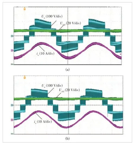
As shown in Fig. 8, the rectifier capability is verified. The input voltage is 220 Vac, the peak input current is 10 A, the output voltage is 400 Vdc, and the FC voltage is 100 V. Fig. 8(a)shows that the voltage ripple across the FC is 12 V and the current ripple is about 1 A. As shown in Fig. 8(b), after adopting the FC voltage balance control, the FC voltage can basically maintain balanced near the reference value. The voltage ripple is 6 V and the current ripple is about 0.4 A. It can be seen that the level stability is improved, and THD is reduced from 6.72%to 4.27%, which verifies the effectiveness of the flying capacitor control strategy.
Fig. 9 shows the waveform of dual control loops rectifier condition, including input currentio, terminal voltageVn, output voltageVdc, and input voltageVac. The input is 220 VAC and the load is 150 Ω. It can be seen that the combination of two bridge arms produces seven voltage levels. The secondorder voltage ripple of the output voltage is less than 20 V,and the current sinusoidal degree satisfies THD=3.89%.
▲Figure 8. Voltage and current waveforms of full load: (a) with openloop control and (b) with flying-capacitor (FC) voltage control strategy

▲Figure 9. Experimental waveforms of rectification under dual control loops
Fig. 10 shows the experimental waveform of transient switching. As shown in Fig. 10(a), when the reference voltage changes from 370 V to 400 V, the output voltage reaches the new steadystate value within one period (13 ms) without significant overvoltage. As shown in Fig. 10(b), in the case of full load switching to half load, the amplitude of AC stabilizes at 1/2 of its original value after a short fluctuation. Transient experimental results show that the closed-loop control strategy has good dynamic response performance.
The experimental waveform under the DC input condition is shown in Fig. 11, where the input voltage is 120 V and the output voltage is 200 V. The bridge arm voltage can be composed of two levels, namely, 100 V and 200 V. Therefore, the feasibility of the control strategy is verified.

▲Figure 10. Dynamic characteristic test waveforms: (a) reference voltage value changing from 370 V to 400 V and (b) full load switching to half load

▲Figure 11. Experimental waveform under a direct current (DC) input case
4 Conclusions
To achieve low common-mode voltage and high power density, this paper proposes a multilevel PFC topology suitable for the communication power supply of 5G base stations. It is a hybrid topology consisting of a five-level ANPC bridge and a diode bridge. A 1 kW experimental prototype is established, which verifies the proposed working principle and control strategy.
Using the modulation strategy of PS-PWM, the converter produces seven levels while the dv/dtis reduced toVdc/7,which greatly inhibits the common-mode voltage and reduces the leakage current. Moreover, by adjusting the redundancy switching state action time to balance the flying capacitor voltage, the total harmonic distortion can be suppressed by less than 4%. A dual closed loop system with PI control of the voltage outer loop and quasi-proportion resonant (quasi-PR) control of the current inner loop is used to realize zero static error tracking. The output voltage is stable within an allowable deviation range, and the control performance is great. Furthermore, the AC and DC input switching is realized to ensure the reliability and flexibility of the power supply.
杂志排行

ZTE Communications的其它文章
- Table of Contents, Volume 21, 2023
- Special Topic on 3D Point Cloud Processing and Applications
- Beyond Video Quality: Evaluation of Spatial Presence in 360-Degree Videos
- Mixed Electric and Magnetic Coupling Design Based on Coupling Matrix Extraction
- Incident and Problem Ticket Clustering and Classification Using Deep Learning
- Research on Fall Detection System Based on Commercial Wi-Fi Devices