氧原子吸附调控蓝磷/石墨烯异质结构的肖特基势垒
2023-10-19段汪洋程悦桓胡吉松马新国
段汪洋 程悦桓 胡吉松 马新国 裴 玲*,
(1湖北工业大学理学院,武汉 430068)
(2湖北省能源光电器件与系统工程技术研究中心,武汉 430068)
(3华中科技大学光学与电子信息学院,武汉 430068)
0 Introduction
Phosphene has attracted attention due to its extremely high carrier mobility.It has an excellent performance in the fields of electrocatalysis[1],photovoltaic power generation[2],energy storage[3]and transistors[4].Besides,it is a strong candidate for the next generation of nano-electronic devices.There are theoretically 9 forms of phosphorene monolayer,includingα-P (black phosphorus)andβ-P(blue phosphorus,BP)[5].Based onη-P andθ-P among them,five new and dynamically stable phosphene heteromers were discovered[6],single crystal violet phosphorus has also been synthesized[7].Phosphorus atoms in a single-layer phosphorene interact with each other through covalent interaction and form a six-membered ring,which is in the form of folds and layers.The layers are combined by van der Waals forces.It′s noteworthy that single-layer blue phosphorus has the same stability as the most stable black phosphorus,has a carrier mobility similar to graphene,and exhibits a wider band gap than them,so it can be used to fabricate transistors[8-9].In recent years,fieldeffect transistors(FETs)based on monolayer blue phosphorus were reported,which showed a high on/off ratio exceeding 350 due to the low contact resistance between the metallic and semiconducting nanoribbons[10-11].Therefore,the development of FETs based on phosphorene will be a trend of electronic devices in the future.
In a device with phosphorene as the channel,a Schottky barrier is often formed at the interface of metal electrodes and phosphorene,which would reduce the carrier injection efficiency[10].In order to explain and address these issues,for example,five representative metal systems such as Au(111),Ag(111),Al(111),Co(111),Sc(0001)[12]and graphene (Gr) heterojunction[13]have been employed to reduce the Schottky barrier height (SBH).Although much research in FETs based on phosphorene has been done,another remarkable fact is that most of them are n-type FETs (n-FETs),and the fabrication of p-type FETs (p-FETs) remains a great challenge.The conducting channel of a FET transports electrons or holes,which depends on whether the SBH is smaller relative to the conduction band minimum (CBM) or the valence band maximum (VBM),respectively,after the Fermi levels of metals and semiconductors are in equilibrium[14].However,due to the complicated interface interaction of the metal/semiconductor,the ideal metal-semiconductor interface is difficult to obtain for the inevitable chemical disorder and Fermi pinning[15-17].Another crucial case according to theoretical calculations is that the p-type Schottky contact appears at the interface with Pd and Sc,BP monolayer forms n-type Schottky contact with Au,Ag and Al,whereas,there are some differences in the Lateral Schottky barrier of the BP transistors with metal electrodes[10-12].On the whole,these studies show that it is relatively difficult to design phosphorene/metal contacts with a low SBH,which limits the development of phosphorene-based FETs.
As experiments and theories improve by leaps and bounds,much research has been carried out to solve this problem.What is known to us is that twodimensional (2D) materials enjoy numerous exceptional advantages over conventional materials on a quantum scale,for instance,graphene has lower losses and higher carrier mobility[18].Recently,it was accounted for that a heterostructure can be changed from a n-type Schottky contact to a p-type Schottky contact with increasing of compressive strain[19].Afterwards,Li et al.[13]affirmed that the electric field was compelling to tune the Schottky barrier for the BP/Gr interface,which can change the n-type into the p-type.Thus,graphene can be used as a low-resistance contact material to replace noble metals.And it is noteworthy that,Liang et al.reported a high-performance anisotropic graphene/black phosphorus heterostructure with promising potential applications in electronic devices[20-22].These achievements provide ideas for us to tune the Schottky barrier of the BP/Gr heterostructures by Odoped.In this work,first-principles calculations on the BP/Gr heterostructures with different concentrations of the O-doped at the interface were performed to explore the interface interaction and electronic properties.Additionally,the charge density difference and work function were used to check the redistribution of interfacial charges and determine the type and height of the Schottky barrier.
1 Calculation methods and models
All calculations were performed using Ultrasoft Pseudopotentials (USP) and using the Generalized Gradient Approximation (GGA)-Perdew Burke Ernzerhof (PBE)[23]form based on the CASTEP[24]implementation of the Generalized Gradient Approximation in Density Functional Theory (DFT) exchange and association.In the USP calculations,a mixed semi-empirical solution of the Grimme[25]and Ortmann-Bechstedt-Schmidt (OBS)[26]schemes is provided to introduce the correct description of van der Waals (vdW) interactions.The dispersion-corrected total energyEtotis represented asEtot=EKS-DFT+EvdW,whereEKS-DFTis the normal Kohn-Sham DFT energy andEvdWis the dispersion correction.In general,semiempirical methods are often used to balance the cost of dispersion terms in firstprinciples calculations with the need to improve nonbonded interactions in the standard DFT descriptions[27].The selected valence atomic configurations are 2s22p2for C,2s22p4for O,and 3s23p3for P.All models were geometrically optimized using the BFGS algorithm,the cutoff energy was set to 350 eV,and the Monkhorst-Packkmesh of 3×3×1 was used[28].The selfconvergence precision was 2.0×10⁻⁵eV per atom,the interatomic force field convergence precision was 0.5 eV·nm-1,the maximum stress was 0.1 GPa,and the maximum displacement was set to 2.0×10⁻⁴nm.
Before exploring the performance of the BP/Gr heterojunction,we optimized the lattice constants of BP (space group:P3m1;a1=b1=0.327 nm) and graphene (space group:P6/mmm;a2=b2=0.247 nm),which were consistent with the previous theory similar to the experimental data (BP:a1=b1=0.338 nm[29-30],GR:a2=b2=0.246 nm[31]).BP monolayer is a novel two-dimensional semiconductor material with a monolayer thickness of 0.124 nm.We used blue phosphorus with 3×3×1 supercells and graphene with 4×4×1 supercells to construct heterojunctions,and established a vacuum layer of no less than 1.5 nm along thez-direction for the separation period images to isolate the slab as the boundary condition.In this structure,1-3 O atoms are adsorbed inside the interface of BP/Gr heterojunction,and the structure for different doping concentrations is shown in Fig.1.For simplicity,the BP/Gr heterojunctions with O concentration (O/P ratio) of 0%,5.56%,11.11%,and 16.67% are denoted as BP/Gr,BP/Gr-1O,BP/Gr-2O,BP/Gr-3O.The lattice mismatch ratio is defined asσ=|a1-a2|/a1,wherea1anda2are the lattice constants of blue phosphorus and graphene,respectively.Table 1 shows that the lattice mismatch ratio of the model is 0.714%,a low 5% of required[27].It was found that the structure was severely distorted,with the increasing of concentration of adsorbed oxygen atoms on the blue phosphorus surface in the interface.Wavy graphene can be stretched to about 30%,because 2D materials can withstand very strong stretching and squeezing[32].
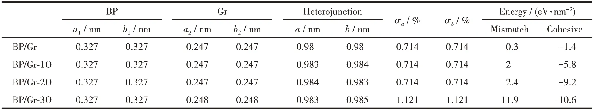
Table 1 Mismatch energies and cohesive energies of BP/Gr heterojunctions with different proportions of the O-doped
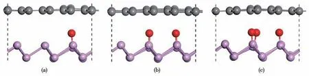
Fig.1 Side views of BP/Gr heterostructures with different proportions of the doped O after geometric optimization:(a)BP/Gr-1O;(b)BP/Gr-2O;(c)BP/Gr-3O
2 Results and discussion
2.1 Interface stability
The interfacial formation energies of heterojunctions at different interlayer distancesdare calculated by using two dispersion correction methods,respectively.The interfacial formation energy of heterojunctions can be calculated as
whereE(BP/Gr),E(BP) andE(Gr) represent the total energies of the interface,the BP sheet and Gr sheet,respectively[33-35].Fig.2 shows that the most stable interlayer distance obtained by the Grimme dispersion correction method is 0.34 nm,while the most stable interlayer distance obtained by the OBS dispersion correction method is about 0.32 nm or 0.34 nm.This result is consistent with the results for 0.34 nm,which is similar to the previous theoretical and experimental results[19,36].
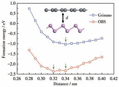
Fig.2 Distance and interface formation energy of heterojunctions interlayer calculated by two dispersion correction methods
The interlayer interactions of a heterostructure have a huge impact on electronic structure.In order to obtain a stable geometrical structure of BP/Gr heterostructures,the interfacial cohesive energy between BP sheet and Gr is expressed as:
whereE(BP/Gr),E(BP) andE(Gr) represent the relaxed BP/Gr heterostructure,the total energy of isolated BP and Gr,respectively.Sis the planar region in the interface.From the Eq.3,the negative value of the interface cohesive energy corresponds to the stable interaction between interlayers,and the obtained lower value represents more stable interface geometry.Table 1 shows that the interface cohesive energies of the BP/Gr heterostructures range from -1.4 to -10.6 eV·nm-2,and they can form stable interfacial contacts.
The lattice mismatch energy of the BP/Gr heterojunction under strain can be estimated as:
whereE(BP)a′andE(Gr)a′are the total energies of isolated BP and isolated Gr,respectively,with the same lattice constanta′ of the BP/Gr heterojunction.E(BP)a1andE(GR)a2are the total energies of isolated BP and isolated Gr,after free-geometric relaxation,respectively[37].In addition,S represents the junction area.Table 1 shows that the mismatch energies of the BP/Gr heterostructures with different doping of O atoms range from 0.3 to 11.9 eV·nm-2.The mismatch energies are positive and grow with the increase of the dopant number of O atoms.It shows that the interface structures are deformed to some extent with the dopant of O atoms.
On the surface of the BP monolayer,three types of high symmetry adsorption sites exist: (i) A sites over a P atom; (ii) B sites over the second layer of a P atom;(iii)C sites above the center of three P atoms;as shown in Fig.3.To investigate the favorable adsorption sites,the adsorption energies of O atoms on different sites were calculated.Due to the thermodynamic stability of structures,the atomic chemical potential generally selects the energy of a single atom in a simple substance.Therefore,the chemical potential of O2molecules in a 1 nm3cubic vacuum unit cell is selected,the O=O bond length is 0.124 nm after optimization,and the energy of a single O atom is -434.03 eV.The adsorption energies between O atoms and the BP monolayer are -2.164 eV for the A site,-1.16 eV for the B site,and-1.126 eV for the C site.The adsorption energy of the O atom at the A site is more negative than the B site and C site,and it is indicated that the A site is the most stable O atom adsorption site.
Fig.3 Structures(a)top view,(b)side view and(c)adsorption energy of three sites
2.2 Energy band structure
To understand the vdW interaction on the electronic structure of the interface,we investigated the energy band structures of BP/Gr heterostructures after the geometries were fully relaxed.The energy band structure of the BP/Gr heterostructure was calculated using the GGA - PBE formalism along the path ofM(0 0.5 0)-K(-1/3 2/3 0)-G(0 0 0),as shown in Fig.4.By means of comparative analysis,Fig.4a and 4b present the energy band structure of the isolated BP monolayer and graphene,respectively.As accounts show,the BP monolayer has an indirect band gap of 1.83 eV at the high symmetryKpoint,which is similar to the results obtained by previous researchers[38-39].Besides,the band gap of 2.1 eV for the BP monolayer is obtained by the HSE06 method.Therefore,the GGAPBE formalism is used in subsequent calculations.Fig.4b shows that the Dirac points appears at theKpoints,because of the (bonding)πbands and (antibonding)π* bands of graphene cross at theKpoints.This indicates that graphene is a gapless semiconductor and maintains its metallic character,consistent with previous theoretical findings[40].
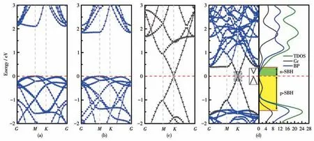
Fig.4 Energy band structures of(a)monolayer BP with the HSE06 method,(b)monolayer BP with the GGA-PBE method,(c)graphene and(d)BP/Gr heterostructure
It can be seen that due to the large equilibrium interlayer distance (0.34 nm) of the BP/Gr heterostructure,the Dirac-cone of graphene and the indirect band gap of BP monolayer still remain unchanged,as shown in Fig.4c.Compared with the band structures of isolated BP monolayer and graphene,the overall shape of the band structure of the BP/Gr heterostructure appears to be a simple sum of each component.Notably,theπandπ* bands separate and form a small bandgap of 7 meV.This may be due to the breaking of structural symmetry and asymmetric potentials[41].The band gap of monolayer BP in contact with graphene hardly changes,indicating the existence of weak vdW interaction between different layers,and maintaining its inherently excellent electronic properties.
To realize more efficient logic devices based on phosphorene,it is necessary to fabricate n-type and ptype FETs with low SBH.According to the Schottky-Mott model at the metal/semiconductor interface[42],the n-type Schottky barrier height (n-SBH) is defined by the energy difference between the CBM level and the Fermi level.Likewise,the p - type Schottky barrier height(p-SBH)can also be expressed as the energy difference between the VBM level and the Fermi level.Therefore,it is worth noting that the sum of n-SBH and p-SBH is equal to the band gap of the BP monolayer in the interface,namely,|n-SBH|+|p-SBH|=Eg(BP),as shown in Fig.4c.Obviously,the pristine BP/Gr interface here has an n-SBH of 0.39 eV,which is basically consistent with other results.Here,we constructed BP/Gr heterostructures with different ratios of oxygen dopants to explore the effect of oxygen doping on the electronic properties of the interface.Fig.5 presents the energy band structures of BP/Gr heterostructures with different concentrations of the O doped inside the interface.We can clearly see a slight change in the band shape of the heterostructure,but an obvious change in the type and height of the Schottky barrier.
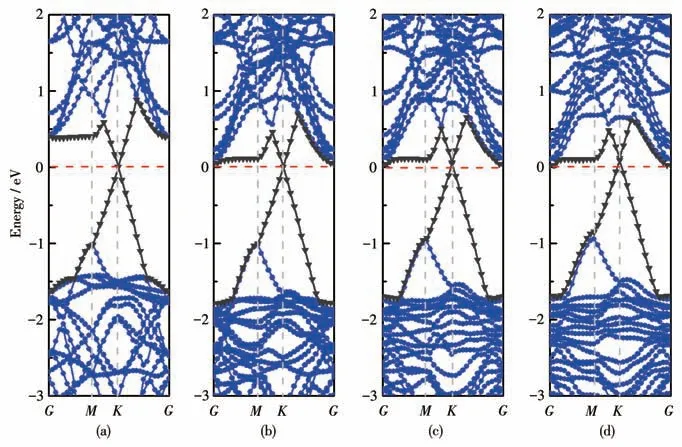
Fig.5 Energy band structure of BP/Gr heterostructures with different proportions of the O atom doped:(a)0%;(b)5.56%;(c)11.11%;(d)16.67%
As the concentration of O doped (O/P ratio,nO/nP)increases from 0% to 16.67% in the interface,the Fermi level of graphene decreases relatively gradually.The energy level of the BP monolayer shift upward gradually,as shown in Fig.5a-5d.The total density of states (TDOS) and partial density of states (PDOS) of the BP/Gr heterostructure with O atoms doped were calculated,as shown in Fig.S1 (Supporting information).Fig.S1a-S1d show that the PDOS of graphene remains not change.In addition,O doped makes the P3pstates of the BP layer move to the left,and the movement is reduced when three O atoms are doped.It can be seen that the deeply effect of O doped on the electronic properties.
A Schottky barrier is formed at this interface between graphene and BP monolayer.The SBH of the BP/Gr heterostructure was quantitatively characterized,and the changes of CBM,VBM and band gap with the doping ratio of O atoms were investigated.Fig.6 shows the dependence of SBH on O atoms doped,which suggests that the Schottky barrier can be tuned by the doped concentration of O atoms.When the dopant concentration is 0%,the Fermi level is closer to the CBM of BP and farther away from its VBM,with a p-SBH of-1.44 eV and an n-SBH of 0.39 eV.With the increase in the concentration of the O dopant inside the interface,the CBM of BP moves downward to the Fermi level,meanwhile the VBM first moves downwards and then moves upwards gradually.It is worth noting that O doped reduces both n-SBH and |p-SBH|,but with the increase of O doped concentration,n-SBH keeps at a low value,while |p-SBH| reduces.When the proportion of the interfacial selenium dopant is increased from 5.56% to 16.67%,the n-SBH of this system is almost unchanged,and the p-SBH is changed from -1.64 eV to -1.48 eV.Therefore,the Schottky barrier of BP/Gr heterostructure can be tuned by O atoms doped.
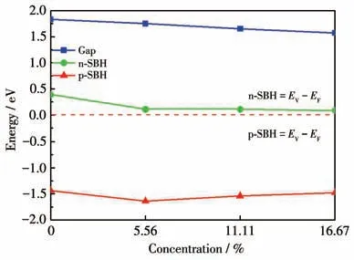
Fig.6 Dependence of SBH on different concentrations of the O atoms doped inside the layer
2.3 Work function
In order to investigate the effect of O atoms doped on the Schottky barrier height at different concentrations,the work functions of BP monolayer,graphene and the BP/Gr heterostructures have been calculated.The work function is defined as follows:
whereEvacis the energy of a stationary electron in the vacuum near the surface andEFis the Fermi level.On the basis of Eq.4,the calculated work functions for BP monolayer,graphene,BP/Gr heterostructure,BP/Gr-1O,BP/Gr-2O and BP/Gr-3O are 5.99 eV,4.12 eV,4.34 eV,3.92 eV,4.02 eV and 4.09 eV,respectively.The presence of a potential difference of 12.55 eV in the heterojunction results in a strong electrostatic field at the interface,which facilitates the separation of electron and hole pairs,as shown in Fig.7 and Fig.S2.The type and height of the Schottky barrier depends on the position of the CBM and VBM at the Fermi level,therefore,they can also be modulated with changes in the work function.However,due to the mechanism of Fermi-level pinning at the BP/graphene interface,the p-orbital of the phosphorus atoms fixes the Fermi level close to the conduction band,leading to an n-type Schottky barrier[19,43].
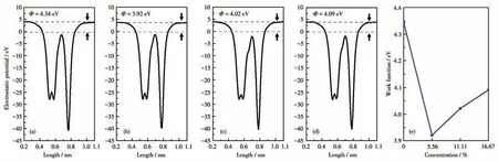
Fig.7 Calculated electrostatic potentials for(a)BP/Gr heterostructure,(b)BP/Gr-1O,(c)BP/Gr-2O,(d)BP/Gr-3O and(e)plots of the O concentration on the work function tunability of BP/Gr heterostructures with O atoms doped inside the interface
To understand how the Fermi level of the BP/Gr heterostructures varies with the concentration of O atoms doped,the work function of BP/Gr heterostructures has been calculated.As shown in Fig.7,the doping of O reduces the work function of the heterojunction,but with the increase of the dopant concentration,the work function of the heterojunction gradually increases.This trend is similar to that of the Schottky barrier.Therefore,the more the curve changes,the more pronounced the adjustment will be,which is exactly what we need to achieve.Obviously,in this modulation case,a lower p-SBH can be obtained by further increasing the concentration of oxygen dopant in the interface,which will facilitate the fabrication of low-power and high-performance p-FETs.
2.4 Mechanism of tuning the Schottky barrier
The formation of heterostructures can alter the electrical properties of heterostructures and BP monolayer or graphene,due to interlayer interactions and interfacial charge redistribution.Therefore,we calculated the three-dimensional (3D) charge density difference,revealing the interlayer charge transfer and separation between the BP monolayer and the graphene surface.And the 3D charge density differences of BP/Gr heterostructures with different concentrations of the O doped at the interface were also calculated,as shown in Fig.8.The charge density difference,Δρ=ρBP/Gr-ρBPρGr,is obtained by subtracting the electronic charge of the BP/Gr interface from that of the corresponding isolated BP monolayer and graphene.Here,ρBP/Gr,ρBPandρGrare the charge densities of the BP/Gr heterostructure,isolated BP monolayer and graphene.It can be seen that the charges of BP and graphene at the interface are redistributed by forming electron depletion(yellow areas) and accumulation (blue areas) in the space with respect to isolated BP and graphene.The surface of the BP layer gathers more negative charges to enhance its work function and the graphene layer gathers positive charges,which leads to the formation of a built-in electric field at the interface.Combined with the calculation results of state density,mismatch energy and cohesion energy,after the adsorption of O atoms by heterojunction,the influence of O atoms on the valence band is more obvious,and with the increase of O adsorption concentration,the mismatch energy gradually increases and the cohesion energy gradually decreases,and the system becomes more and more stable.
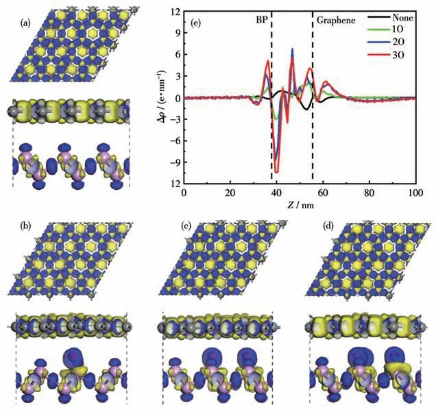
Fig.8 Top and side view of the 3D charge density difference for(a)BP/Gr heterostructure,(b)BP/Gr-1O,(c)BP/Gr-2O,(d)BP/Gr-3O;(e)Planar electron density differences along the z direction of BP/Gr heterostructures with different concentrations of the O adsorption doped inside the interface,in which positive and negative values represent electron accumulation and depletion in the space with respect to isolated BP and graphene,respectively
In order to quantitatively analyze the redistribution of interfacial charges at the interface,the planar averaged charge density differences along thezdirection of BP/Gr heterostructures are calculated,as shown in Fig.8e.The positive values indicate electron accumulation,while the negative values represent the depletion of electrons.The distribution of interfacial charges depends on the concentration of the O dopant.Before adsorption doping,electrons are transferred from graphene to BP.After adsorption doping,the electron transfer situation is torsional,with the concentration of the O dopant inside the interface increasing,the interlayer vdW force has been strengthened,and the interlayer distance between BP and graphene have been shortened,progressively,leading to more electron transfer from BP layer to the graphene.
The results of Mulliken population analysis show that the charge transfer and redistribution inside and outside the interface varies with O atoms doped.After adsorption,the average Mulliken population of P atoms(BP) increases from 0.052e to 0.146e with the increase in the concentration of the O doped inside the interface.The electron transfer from the BP monolayer to the O atoms,which causes the Fermi level of the heterostructure to move downward.The increase in the number of transferred electrons in the interlayer leads to a transition from the n-SBH to p-SBH,which is consistent with the analysis of the work function.Moreover,more electrons are transferred from P to O.It turned out that larger Mulliken populations of P,C and O atoms inside the interface are found which produce a great interface interaction between two constituents,which is in agreement with the calculated cohesive energy mentioned above.It can be considered that the redistribution of the interfacial charge leads to the shift in Fermi level,and thus determines the type and height of the Schottky barrier.
3 Conclusions
In summary,the microscopic mechanisms of interface interactions by O adsorption doped and their influence on the electronic structures of the BP/Gr heterostructure have been investigated by DFT calculations in detail.The vdW forces between BP and graphene overcome the energy mismatch,and make the heterostructure bind tightly.Moreover,the intra-interface O adsorption doped has a great influence on the interlayer interaction and electronic properties.In addition,the height of the Schottky barrier can be tuned by O adsorption doped inside the interface.With the increase in the concentration of the O doped inside the interface,the p - SBH transforms from -1.64 eV to-1.48 eV.Especially,a smaller p-type Schottky barrier can be achieved with the increase of the concentration of O adsorption doped,which is a significant requirement for a highly efficient hole transfer at the interface.By analyzing the work function and charge density difference,it is confirmed that the redistribution of interfacial charges leads to the shift of the Fermi level,and then determines the height of the Schottky barrier in the BP/Gr heterostructure.In summary,our results reveal that asymmetric O adsorption doped is quite a promising strategy to tune the Schottky barrier of the BP-based heterostructure.
Supporting information is available at http://www.wjhxxb.cn
