控制碘化铅形貌两步连续刮涂法大面积制备甲脒基钙钛矿薄膜
2023-03-15文永涛李静高晓峰田聪聪朱昊余国木张晓俐HyesungPark黄福志
文永涛,李静,高晓峰,田聪聪,朱昊,余国木,张晓俐,Hyesung Park ,黄福志,*
1武汉理工大学材料复合新技术国家重点实验室,武汉 430070
2先进能源科学与技术广东省实验室佛山分中心佛山仙湖实验室,广东 佛山 528216
3武汉理工大学材料科学与工程国际化示范学院,武汉 430070
4郑州大学材料科学与工程学院,郑州 450001
5 Department of Materials Science and Engineering, Graduate School of Semiconductor Materials and Devices Engineering,Perovtronics Research Center, Low Dimensional Carbon Materials Center, Ulsan National Institute of Science and Technology,Ulsan 44919, Republic of Korea
1 Introduction
Perovskite solar cells (PSCs)have attracted much attention due to their high power conversion efficiency (PCE), printability,and low-cost preparation1-7. The certified PCE of PSCs has exceeded 25%8, which shows a huge prospect for future commercial applications9. However, the reported highperformance devices were all prepared through spin-coating methods, normally using anti-solvent strategies to prepare highquality perovskite films10-12. In fact, the photoelectric performance of large-area PSCs prepared by a combination of spin-coating and anti-solvent will be greatly reduced13,14.Therefore, a process that is compatible with large-area highquality perovskite films is currently in urgent need to accelerate the process of industrialization15.
Blade-coating method is a process with simple operation and efficient material utilization, and has been widely regarded as an effective method for preparing large-area thin films16-24. For a blade-coating process, the substrate is firstly placed on a platform, and then the precursor solution is coated on the substrate by moving the blade to form a wet film. After the solvent evaporates, the solute crystallizes on the substrate to form a thin film. The quality of the perovskite film can be improved by changing the precursor solution composition or through solvent engineering25,26. Therefore, a large amount of research has focused on one-step coating of MA-based perovskites that are quite easy to control their crystallization27,28, but there are few studies on FA-based perovskites that are more stable and efficient29-33. The main reason is that the nucleation and growth process of FA-based perovskites are difficult to control through the one-step bladecoating process34.
In contrast, the two-step sequential blade-coating deposition method is much easier to handle, as it does not involve the nucleation process of the perovskite. The two-step method first deposits the PbI2film on the substrate, and then second coating of (FAI)undergoes continuous solid-phase reaction with PbI2to transform into a perovskite film35,36. The interaction process between PbI2and FAI molecules effectively solves the uncontrollable nucleation issue of FA-based perovskites in the one-step process. Therefore, the two-step deposition is considered to be a more controllable and reliable method for uniformly preparing thin films on a large area. One of the main problems in the two-step process is that the compact PbI2film is not conducive to the complete conversion of perovskite as the FAI molecules are hard to diffuse to the bottom of the film.Therefore, a lot of research is devoted to controlling the morphology of PbI2to form a porous structure, providing nanochannels for FAI diffusion, and also increasing the specific surface area between PbI2and FAI molecules to facilitate the reaction. For example, Liet al.37adopted multistep annealing method to deposit a porous PbI2film and improved the quality and uniformity of perovskite films. Choyet al.38used the PbI2precursor solution to incorporate a small amount of reasonably selected additives to form a self-assembled porous PbI2, which significantly promoted the conversion of perovskite without any PbI2residues. Huanget al.39reported a vertically aligned PbI2film grown from an ionic liquid. The vertically grown structure has numerous nanoscale ion channels, which facilitates the rapid and stable conversion to FAPbI3, and finally achieves 24.1% PCE and excellent thermal stability. For the two-step process, it has been strongly proved that controlling the morphology and structure of PbI2is essential for the preparation of high-quality perovskite films. However, high-performance devices are all based on spin-coating, and there are relatively few research reports on the scalable process, such as blade-coating. We prepared the perovskite film by a two-step blade-coating method and found that the deposited PbI2film with layered crystals is not conducive to the second step of the reaction. Therefore, how to realize the PbI2film with regular and continuous nanochannels is extremely essential for the sequential bladecoating method. In this work, THTO is introduced into the PbI2N,N-dimethylformamide (DMF)solution to control the crystallization of PbI2, which results in a continuous porous layer composed of vertical packed flaky PbI2nanocrystals. This strategy facilitates the diffusion of organic amine salts and addresses the issue of incomplete reaction between PbI2and organic amine salts in the two-step method. In addition, highquality perovskite films were prepared by combining the blade coating method to solve large-area printing.
2 Experimental
2.1 Materials
SnCl2·2H2O was purchased from Aladdin, and urea was purchased from Alfa Aesar. DMF, isopropyl alcohol (IPA), and dimethyl sulfoxide (DMSO)were purchased from Sigma-Aldrich. Lead iodide (PbI2), FAI and methylammonium chloride(MACl)were purchased from Xi’an Polymer Light Technology Corp. THTO was purchased from Acros. Spiro-OMeTAD was purchased from Shenzhen Feiming Science and Technology Co.,Ltd.
2.2 Precursor preparation
The PbI2solution was prepared by dissolving 600 mg PbI2powder in mixed solvents (DMF:additives). For the preparation of the solution of organic amine salts, 60 mg FAI and 15 mg MACl were dissolved in 1 mL IPA.
2.3 Device fabrication
F-doped SnO2glass substrates (FTO)were etched by femtosecond laser, and followed by ultrasonic cleaning through detergent, deionized water and ethanol for 20 min, respectively.The substrates were treated by ultraviolet (UV)light for 15 min before deposition of SnO2. The SnO2film was prepared by chemical bath deposition (CBD)according to our previous report. The perovskite films were deposited on the SnO2substrateviathe two-step sequential blade-coating method in ambient environment. First, 60 μL of PbI2precursor solution (5 cm × 5 cm substrate)was dropped on the substrate to form a horizontal line, and then the coater with the blade height of 0.48 mm above substrate was controlled to move at a speed of 4 mm·s-1. The wet films were dried immediately by air blowing and then annealed at 70 °C for 1 min to dry films. After the substrate cooled down to room temperature, the mixture solution of FAI:MACl (60 mg:15 mg in 1 mL IPA)was bladed onto the PbI2films (generally 80 μL for 5 cm × 5 cm substrate), then annealed at 150 °C for 15 min for perovskite crystallization.After cooling down, a 5 mg·mL-1t-BAI/IPA solution was spun onto the small size blade-coated perovskite films and followed by annealing at 100 °C for 10 min. The Spiro-OMeTAD solution was prepared by dissolving 91.4 mg Spiro-OMeTAD, 35.65 μL 4-tert-butylpyridine, 21 μL Li-TFSI (from 520 mg·mL-1stock acetonitrile solution)and 11 μL FK209 (300 mg·mL-1stock acetonitrile solution)in 1 mL chlorobenzene (CBZ). After stirring adequately, the desired solution was spun onto perovskite films by 4000 r·min-1for 20 s. Finally, about 80 nm Au was deposited by thermal evaporation method.
2.4 Characterizations
The field emission scanning electron microscope (FESEM,Zeiss Ultra Plus)and atomic force microscope (AFM, SPM9700,Shimadzu, Japan)were used to characterize the surface morphology and microstructure of all PbI2films, perovskite films, and device structures. The crystal phase of PbI2and perovskite films was characterized by an X-ray diffractometer(XRD, D8 Advance). The Fourier transform infrared (FTIR)spectra were obtained using Nexus. The steady-state photoluminescence (PL)spectra were characterized by a PL microscopic spectrometer (Flex One, Zolix, China). TheJ-Vcurves of all PSCs were measured in room environment using a Keithley 2400 source meter and an AM 1.5 G solar simulator(Oriel 94023 A, 300 W). A standard silicon cell (Oriel, VLSI standards)was used to calibrate the intensity of light to 100 mW·cm-2. The test scan rates for 0.16 cm2devices and 5 cm × 5 cm modules with an aperture area of 10 cm2were 10 and 50 mV·s-1, respectively. The external quantum efficiency (EQE)was tested using commercial EQE system (Newport).
3 Results and discussion
For the two-step blade-coating process, the most important step is the deposition of PbI2layer. Fig. 1 shows the fabrication process of perovskite filmsviathe blade-coating method from compact-PbI2(labeled C-PbI2)and THTO additive-induced vertical nanochannel-PbI2(labeled NC-PbI2)films.Traditionally, PbI2films are often obtained by volatilizing the solvent through thermal annealing40, but the pores structure are often discontinuous. The main reason is that the PbI2grains are small, and in a certain range, it is still compact PbI2, which affects the permeation of FAI molecules. Thus, the compact PbI2crystals, especially distant from the contact interface, cannot be fully converted into perovskites. While by introducing THTO into the PbI2precursor solution, PbI2will coordinate with THTO molecule which is a sulfur-donor ligand to form coordination complexes PbI2-THTO after volatilization of DMF at 70 °C.THTO acts as a Lewis base additive to alter the crystallization of PbI2, thus inducing flaky PbI2crystals. The vertical stack of the large flaky PbI2grains leads to continuous nanochannel in the films. This structure subsequently offered a widely enlarged contact area to facilitate interfacial reaction with FAI/MACl and greatly improved perovskite crystallization.
Fig. 1 Schematic diagram of the fabrication process of perovskite films via the blade-coating method from C-PbI2 and THTO additive-induced NC-PbI2 films.
Fig. 2a,b shows the scanning electron microscope (SEM)images of the surface and cross-section of the C-PbI2film, where it can be observed that the film is composed of layered, and dense small crystals. In contrast, the NC-PbI2(Fig. 2d,e)films have flaky large grains of PbI2and continuous regular nanochannels. After addition of THTO, the thickness of the NCPbI2film increases from ~370 nm (Fig. 2b)of C-PbI2film to~595 nm (Fig. 2e)due to loose stacking of flaky PbI2that also alters the surface roughness. Fig. S1a,b (Supporting Information)show atomic force microscopy (AFM)images of the C-PbI2and NC-PbI2films, respectively. The roughness (Rq)of the films increases from 16.6 nm for C-PbI2to 28.0 nm for NC-PbI2. After the second blade-coating step of the organic mixed salts of FAI/MACl, the PbI2film is converted to perovskites. From the cross-sectional SEM images of the perovskite films (Fig. 2c,f), it can be observed that the perovskite film converted by C-PbI2consists of several small grains in the normal direction and has a large amount of PbI2residual at the interface, while the perovskite film converted by NC-PbI2has a single large grain in the normal direction and no residual PbI2.The single-grain structure can reduce the number of grain boundaries in the film, facilitate carrier transport and increase carrier lifetime, thereby improve photoelectric conversion performance. The vertical stacked flaky PbI2in the NC-PbI2film not only offers continuous nanochannel for FAI/MACl diffusion,but also has a greatly enlarged surface area available for the subsequent reaction, thus forming a complete reacted large grain perovskite.
To reveal the mechanism for the generation of vertical nanochannels in NC-PbI2thin films, the pure PbI2·THTO solution was used for blade-coating. The corresponding X-ray diffraction (XRD)results of the obtained film (Fig. S2)show that a strong PbI2·THTO complex peak appeared at 7.8°. The complex crystals are aligned vertically in the film direction as shown in the cross-sectional SEM images (Fig. 2i). In addition,Fig. 2j shows the XRD results of PbI2(DMF/DMSO)and PbI2(DMF/THTO)films. It can be clearly observed that a peak at 7.8° and a PbI2phase peak at 12.7° appear on the PbI2-DMF/THTO films. While the PbI2-DMF/DMSO films only have a PbI2peak at 12.7°. Therefore, it can be PbI2·THTO complex proved that the vertical nanochannel inside the NC-PbI2films are causedviathe complex phase generated by the complexation of PbI2and THTO.
Fig. 2 The surface and cross-sectional SEM images of the blade-coated PbI2 films:(a, b)C-PbI2 and (d, e)NC-PbI2.The cross-sectional SEM images of the blade-coated perovskite films converted from different blade-coated of (c)C-PbI2 and(f)NC-PbI2 films. FTIR spectra of (g)liquid DMSO (blue), PbI2 (DMF/DMSO)films (red)and (h)liquid THTO (blue), PbI2 (DMF/THTO)(red).(i)The cross-sectional SEM images of the blade-coated PbI2 (THTO)films. (j)XRD patterns of the C-PbI2 and NC-PbI2 films.
The most striking difference in the XRD patterns between CPbI2and NC-PbI2can be explained by “bond unsaturation”41.For this family of similar molecules, such as DMSO and THTO,the lower the Mayer bond order (MBO)and the higher the bond unsaturation value, the stronger complexing ability. It is found that the bond unsaturation 0.52 of THTO is higher than the bond unsaturation 0.49 of DMSO shown Table S1. Therefore, THTO have strongly interacts with the Pb2+ion forming PbI2·THTO complex after drying. In addition, Fig. 2g, h show the FTIR spectra for liquid DMSO (blue), PbI2-DMF/DMSO (red)films and liquid THTO (blue), PbI2-DMF/THTO (red)films,respectively. The stretching vibration peak of S=O appears at~1022 cm-1for liquid DMSO, shifting to ~974 cm-1for the PbI2-DMF/DMSO films, and the peak of liquid THTO appears at~1008 cm-1, shifting to 933 cm-1for the PbI2-DMF/THTO films.The more intense low-frequency shift (75 cm-1)for the PbI2-DMF/THTO film displays the formation of stronger coordination bond between PbI2and THTO than that of DMSO(48 cm-1)42. These results effectively demonstrate the strong interaction between PbI2and THTO, which is the cause forming the PbI2·THTO complex.
Fig. 3a,b shows the XRD pattern of the perovskite films with various annealing time converted from blade-coated C-PbI2and NC-PbI2films, respectively. It is found that the un-annealed perovskite films converted from C-PbI2have a PbI2peak at 12.7°, while the films converted from NC-PbI2have no PbI2peak. This strongly proves that the NC-PbI2films can promote the complete reaction between PbI2and FAI without residual PbI2. In addition, the diffraction peaks of PbI2in the C-PbI2and NC-PbI2-converted perovskite films are continuously strengthened with the annealing process. This is attributed to the introduction of MACl that results in the decomposition of MA components during annealing43. Therefore, for the fully annealed perovskite film, the PbI2in the C-PbI2conversionbased perovskite film is excessively residual, which contains unreacted PbI2and the PbI2generated by the decomposition of the MA-based perovskite during annealing. For the fully annealed perovskite film based on NC-PbI2conversion,however, the diffraction peak intensity of the (110)plane of perovskite is significantly stronger than that of PbI2, implying higher perovskite crystallinity and moderate of PbI2residues(Fig. S3). Moderate PbI2residues can effectively passivate defects and enhance the photovoltaic performance of PSCs,while excess PbI2can degrade the device performance44-46.Therefore, the quality of perovskite films obtained based on NCPbI2conversion will be significantly improved. The perovskite grains converted from the C-PbI2(Fig. 3c)is much smaller than that from the NC-PbI2films (Fig. 3d). The average grain sizes of perovskite converted from the C-PbI2and NC-PbI2films are~300 nm (Fig. S4a)and ~700 nm (Fig. S4b), respectively.Although the NC-PbI2film has a rougher surface, the converted perovskite film becomes much smooth due to the sufficient reaction. The roughness of the perovskite films obtained from Fig. S1c,d for the C-PbI2and NC-PbI2are 70 and 54 nm,respectively. This confirms the importance of controlling the morphology of the PbI2films on the crystallization of perovskite.
Fig. 3 The XRD patterns of the perovskite films with different annealing time converted from blade-coated of (a)C-PbI2 and (b)NC-PbI2 films.The surface SEM images of the perovskite films converted from (c)C-PbI2 and (d)NC-PbI2 films. (e)Steady-state PL spectra and(f)TRPL spectra of the blade-coated perovskite films converted from different PbI2 films.
To investigate the charge carrier dynamics, the steady-state photoluminescence (PL)spectra (Fig. 3e)clearly observe that the NC-PbI2based perovskite film sample exhibits higher fluorescence intensity, which indicates that the quality of the perovskite films is greatly improved. In addition, time-resolved photoluminescence (TRPL)measurements are employed to evaluate the recombination behavior of the photoexcited carriers in the perovskite films (Fig. 3f). Correspondingly, the decay constants indicating the radiative recombination of free charge carriers that originate from the bulk perovskite obtained by a double exponential fitting increases from 0.80 to 1.86 µs for the perovskite films based on C-PbI2and NC-PbI2. The reason for the prolonged life is that after the introduction of THTO, the nanochannel structure produced in the PbI2film significantly increases the grain size of the subsequently converted perovskite film, and reduces the concentration of surface and grain boundary defects.
To evaluate the effect of the bladed-coated different PbI2morphologies on the device performance, the converted perovskite films are made into compete devices with a structure of FTO/SnO2/Perovskite/Spiro-OMeTAD/Au as shown in Fig.4a. The current density-voltage (J-V)curves of the champion devices fabricated based on the C-PbI2and NC-PbI2are shown in Fig. S5a,b, respectively, and the corresponding photovoltaic characteristic distributions are shown in Figs. 4b and S6. The PCE in a reverse scan of the champion NC-PbI2device is 22.21% with an open-circuit photovoltage (Voc)of 1.13 V, a short-circuit current density (Jsc)of 24.56 mA·cm-2, and a fill factor (FF)of 0.80, which is the best reported PCE in literature based on the two-step sequential blade-coated perovskites as shown in Table S2. Compared with the C-PbI2device with the best PCE of 20.03% as shown in Fig. S5a, the photovoltaic performance has been greatly improved, indicating the essential of the improvement of PbI2morphology for the preparation of highperformance devices although it still has hysteresis.
To further eliminate the hysteresis, a large cation based iodide salt, tert-butylammonium iodide (t-BAI), was used to engineer the interface, which has been proved to be effective in suppressing hysteresis47. Fig. 4c shows theJ-Vcurve of the champion device with the assisted interface treatment oft-BAI/IPA solution. Under the reverse scan, the PCE of the device is as high as 22.77% with aJscof 24.66 mA·cm-2, aVocof 1.14 V, and an FF of 0.81, and the forward scanning efficiency is 21.30%. The external quantum efficiency (EQE)measurement(Fig. 4d)of the corresponding champion device was also performed to confirm the photocurrent, and the integrated current density is 24.38 mA·cm-2, which matches well with theJ-Vresults. Fig. 4e shows the steady-state power output of the champion device. Under a bias of 0.99 V, the steady-state output current density is 21.42 mA·cm-2, and the corresponding efficiency is 21.21%.
Stability is also one of the essential properties of PSCs. Fig.S7 shows the storage stability of unencapsulated devices prepared with different PbI2morphologies at room temperature with a relative humidity of (20 ± 5)%. The NC-PbI2device retains more than 90% of the initial PCE of after being stored for 1000 h, showing excellent environmental stability, while the CPbI2device only remains ~70% of the initial efficiency. In addition, the thermal stability of the devices without encapsulation under indoor conditions of 50 °C with a relative humidity of (20 ± 5)% was also tested. As shown in Fig. 4f, the NC-PbI2device exhibits an excellent thermal stability, retaining more than 80% of the initial PCE after more than 800 h under ambient air conditions, whereas the C-PbI2device only remains about 50% of the initial PCE. The improved stability is due to the controlled microstructure of the PbI2film, which is beneficial to the complete conversion of high-quality perovskite.
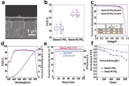
Fig. 4 (a)The cross-sectional SEM image of a PSC with the structure of FTO/SnO2/Perovskite/Spiro-OMeTAD/Au.(b)PCE statistical distributions of PSCs prepared from different PbI2 films. (c)Photovoltaic J-V curves, (d)EQE spectrum, and(e)the corresponding stable-state current output at the maximum power point of the champion NC-PbI2 device treated with t-BAI.(f)Stability measurements of the non-encapsulated devices based on different PbI2 morphologies at 50 °C in air with a relative humidity of (20 ± 5)%.

Fig. 5 (a)The photos of (i)NC-PbI2 films, (ii)perovskite films, and (iii)perovskite solar module. (b)J-V curves of the optimal 25 cm2 PSMs fabricated from the NC-PbI2 films via the sequential bladed-coating process. (c)The stability measurements of 5 cm × 5 cm module performed in air at room temperature with a relative humidity of (20 ± 5)%.
Finally, to show the scalability, we successfully prepared a large-area perovskite film based on the NC-PbI2through twostep sequential blade-coating. The corresponding 5 cm × 5 cm PbI2film, perovskite film and perovskite solar module (PSM)photos are shown in Fig. 5a. The PSM based NC-PbI2with an active area of 10 cm2shows an outstanding photovoltaic performance (Fig. 5b), with a PCE of 18.65%, aJscof 3.72 mA·cm-2, aVocof 6.65 V, and an FF of 0.75. However, the PSM based on the C-PbI2shows a relatively poor photovoltaic performance (Fig. S8), with a PCE of 15.23%, aJscof 3.70 mA·cm-2, aVocof 6.31 V, and an FF of 0.65. This also further illustrates the control of the morphology of the PbI2film to prepare a high-performance perovskite solar module is an effective strategy. The PSM based NC-PbI2retains 90% of the original PCE after 1000 h storage without encapsulation as shown in Fig. 5c. As shown in Fig. S9, the NC-PbI2PSM exhibits an excellent thermal stability, retaining more than 70% of the initial PCE after more than 800 h under ambient air conditions. Therefore, through the strategy of controlling crystallization of PbI2to obtain optimized microstructure of the PbI2film, the application of two-step blade-coating to prepare the high-quality large-area perovskite film has shown great potential in the upscaling PSMs.
4 Conclusions
In summary, we have successfully prepared high-quality FA-based perovskite layers through the two-step sequential bladecoating method. By introducing the Lewis base THTO into the PbI2precursor solution to control the crystallization of PbI2,vertical nanochannels are self-formed in the PbI2film. The PbI2film with vertical nanochannels provides continuous nanochannels for the penetration of FAI molecules and larger interface reaction area than the compact PbI2film. This method is conducive to the complete conversion of PbI2into perovskite,and the grain size and crystallinity of the perovskite film are greatly improved. A FA-based device with the highest PCE of 22.77% is achievedviathis sequential blade-coating strategy.Large PSMs with the area of 5 cm × 5 cm were also prepared,achieving an efficiency of 18.65%. In addition, unencapsulated small-area devices and large-area modules show excellent stability in ambient air. This two-step sequential blade-coating method has successfully demonstrated in fabrication of largearea high-quality FA-based perovskite films, showing a broad application prospect for the scaling up PSCs.
Acknowledgements:The Analytical and Testing Centre of Wuhan University of Technology and Hubei Key Laboratory of Low Dimensional Optoelectronic Material and Devices, Hubei University of Arts and Science are acknowledged for the XRD and SEM characterizations.
Supporting Information:available free of chargeviathe internet at http://www.whxb.pku.edu.cn.