环境控制与等离子体技术融合对未来高精密抛光难加工材料所构成的挑战
2023-01-28土肥俊郎會田英雄大西修尹韶辉任莹晖
土肥俊郎 , 會田英雄, 大西修, 尹韶辉, 任莹晖
(1.九州大学, 福冈 814-0001, 日本)
(2.长冈技术科学大学, 新泻 940-2188, 日本)
(3.宫崎大学, 宫崎 889-2191, 日本)
(4.湖南大学, 长沙 410082)
(5.株式会社 Doi Laboratory,福冈 814-0001,日本)
1 Introduction
The ultra-precision CMP technology plays an extremely important role in ultra large scale integration (ULSI)devices made of semiconductor silicon (Si), and as a result,LSI devices have made amazing progress[1].This CMP technology serves as a model for advanced surface processing methods for other functional material substrates[2].In the 1990s, CMP technology was applied to the planarization processing method for multi-layer wiring of VLSI devices[3], and now, this planarization CMP technology is essential for advanced semiconductor processes.It is well-known that this CMP technology gives a great business opportunity to related fields in various fields such as processing machine,pads, slurries, cleaning, control and measurement (including endpoint detection)[4].However, extremely large problems have been pointed out in the situation where ultra-miniaturization and high density of ULSI devices are progressing.In other words, as the wiring pattern width is further miniaturized, deep EUV must be used because the exposure wavelength must be made smaller according to the pattern,and the technical and cost limits are approaching.
Therefore, instead of "More Moore," which promotes the degree of integration according to Moore's law, another idea has been highlighted.That is "More than Moore"[5], including three-dimensional devices (3D-IC), new non-volatile memory that replaces DRAM and flash memory[6], high-frequency power devices aiming to improve power efficiency,white LEDs, R&D of many multifunctional devices is required.Next-generation compound semiconductor materials,such as SiC and GaN, are emerging in the spotlight.
As mentioned above, in addition to the situation where Moore's law does not go as it has in recent years[7], the physical limit of silicon has been reached in high frequency /power device systems; therefore, wide-band-gap semiconductor substrates such as silicon carbide (SiC), gallium nitride (GaN) and near-future diamond crystals have been used as next-generation devices, such as light-emitting devices.These substrates have also been attracting attention as green devices[8].To fully exhibit the unique properties of these crystals and apply them as substrates for creating high-quality thin films, it is essential to finish these substrates with high-precision in an ultra-precision shape[9].
Therefore, in the present study, we investigated ultraprecision machining processes for hard-to-process substrates of SiC, GaN or diamond as ultimate devices.The materials to be processed must have the same processing accuracy and atomic order quality as that of the Si wafer for LSI devices.However, because these materials are extremely stable, both mechanically and chemically, they are extremely hard-toprocess and new techniques are required for production.The processing time of the SiC, GaN and diamond substrates, assuming that the processing conditions of Si are applied, are shown in Figure 1, which shows the difficulty of processing these substrates[10].
Here, we consider the processing of hard-to-process single crystal substrates.Generally, mechanical stability makes the mechanical removal of materials extremely difficult.However, chemical stability keeps the surface of the material stable from the chemical reaction between the material surface and the abrasive grain dispersion solution/slurry(chemical dissolution of the surface, softening, formation of the brittle layer, and so on).Therefore, it is extremely difficult to apply chemical mechanical polishing (CMP) owing to the synergistic effect of chemical and mechanical actions, unlike the Si crystal substrate.
Generally, an atomic level processed surface by CMP is created by a mechanism that forms a brittle material surface through chemical action and mechanically minutely removes it with soft abrasive grains or pads[11].Since a hard-to-process single crystal substrate has high hardness and excellent chemical stability, it is not easy to form a fragile layer, but the fragile layer can be formed if it is limited to only the extreme surface.For example, it has been found that the action of generating OH radicals by ultraviolet (UV) irradiation during processing and the action of highly dissolved oxygen in micro-nano bubble water plays important roles in surface modification and reaction promotion[12-13].Further, when con-sidering CMP from the viewpoint of tribology, it is possible that radicals released by the generation of microtriboplasma[14]may contribute to modification of the processed surface or tribo-chemical reaction.Focusing on the formation of such a fragile layer on the extreme surface, optimization of all factors involved in the chemical reaction is required to increase the efficiency of the surface reaction.In other words, while pursuing chemical components (including oxidizers) in the slurry, in addition to conventional efforts such as the use of external energy (such as UV irradiation), the CMP environment (ambient gas in the working section and its pressure, etc.), it is necessary to optimize the processing conditions.
The CMP method is extremely effective and important for obtaining surface planarization.If the planarization is sacrificed to some extent, there is a dry-etching process with high processing efficiency[15].The removal rate in CMP of hard-to-process single crystals is usually several to several hundred nm/h (the difference varies depending on the material), whereas dry-etching method generally has a removal rate 10 to 100 times higher than that of CMP method.Based on this, to create a highly efficient and high-quality surface for hard-to-process materials, considering dry etching method that has a weakness in planarization but high efficiency, and CMP method that has a problem in processing efficiency but is excellent in planarization , we thought about a fusion processing method that takes advantages of each method.
In the present study, unique CMP processing apparatuses that introduced new methods regardless of conventional processing methods were designed and prototyped to find a novel processing technology for next-generation hard-to-process materials.There were two types of devised prototype apparatuses: (i) A closed processing environment control CMP apparatus that performed processing in a chamber that was pressurized with oxygen / air gases[16], and (ii) a plasma fusion CMP apparatus that was assisted during the plasma processing[17].In the former, we also challenged the high-efficiency processing by ultraviolet (UV) irradiation to introduce a photocatalytic reaction in a high-pressure oxygen atmosphere[18].The latter is a processing method that combines the plasma chemical vaporization machining (P-CVM) under atmospheric pressure method[19]and the CMP method,aiming to achieve a synergistic effect that is not a mere summation.The apparatus was designed using the diamond substrate that has the highest hardness on the Earth.
We applied these unique prototype processing apparatuses incorporating these ideas to CMP processing of hard-toprocess material substrates such as SiC, GaN and diamond and investigated the CMP processing mechanism while determining the processing characteristics.
2 Basics of CMP of various hard-to-process substrates
Here, information is provided for polishing hard-to-process materials based on the colloidal silica polishing/CMP characteristics of various materials.
2.1 Colloidal silica polishing / CMP characteristics of various substrates
Figure 2 shows the relationship between the removal rate and processing pressure of colloidal silica polishing /CMP for various materials.The removal rates of all materials are proportional to the processing pressure according to Preston's law.The mechanically soft LiTaO3substrate has a high removal rate.However, the removal rate of the Silicon(Si) substrate is relatively hard even though its chemical activity is high, whereas the processing rate of the sapphire substrate that is mechanically and chemically stable is low[20].

Fig.2 Relationship between removal rate and processing pressure in colloidal silica polishing / CMP for various materials
For the mechanically and chemically stable substrates of GaN and SiC, we investigated the removal rate by changing the pH value of colloidal silica to change the chemical action[21].The processing characteristics of the GaN and SiC are shown in Figures 3 and 4, respectively.From these results, it is shown that even when the material is chemicallystable, the removal rate increases as the pH changes, with the removal rate following Preston's law in proportion to the processing pressure or relative speed.It is difficult to consider the simple chemical surface dissolution because of the processing mechanism of the chemically stable materials, rather it is better to think that the processing is accelerated while forming some type of soft reaction products on the substrate surface[22].

Fig.3 Example of processing characteristics of GaN substrate

Fig.4 Relationship between removal rate and pH value of slurry in SiC substrate (Si surface side) by colloidal silica polishing/CMP
Therefore, from information on the processing mechanism of CMP, it was assumed that the hydrated film or soft oxide film would be promoted while being formed on the extreme surface of the substrate during polishing.Then, by intentionally forming the oxide film on each substrate surface,the processing characteristics were examined.
2.2 Effect of oxidation action during processing
Focusing on the GaN and SiC substrates, which are both hard-to-process materials, an oxide-like film was formed as a reaction product on the extreme surface as described in the previous section[23-24].That is, the GaN substrate (Ga surface side) and SiC substrate (Si surface side)were assumed to have a GaO2film and a SiO2film, respectively.Figure 5 shows an example in which a GaN substrate was annealed in air and then the substrate was polished with colloidal silica.When the annealing temperature was increased, the thickness of the GaO2oxide film that was formed on the surface of the GaN substrate (Ga surface side)increased; therefore, the processing time for the removal of a certain amount was shortened.Figure 6 shows a reference example in which a single crystal Ga2O3substrate was polished with colloidal silica.Unlike the GaO2in Figure 5,Ga2O3is a softer oxide film crystal and the removal rate was more than two orders of magnitude higher[22].
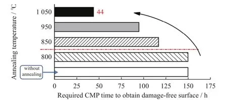
Fig.5 Annealing effect in colloidal silica/CMP characteristics of GaN substrate (CMP characteristics of GaN (Ga surface side) with colloidal silica after annealed GaN substrate)
To confirm this for the SiC substrate, we attempted processing by intentionally forming a SiO2film on the Si surface side of the SiC substrate by thermally oxidizing the SiC substrate.Here, a surface oxide film (thickness of approximately 0.1 μm) on the Si surface side of the SiC substrate was formed by plasma irradiation for 1 min in an oxygen atmosphere.Figure 7 shows an example of the results of processing the Si surface side of a SiC substrate with colloidal silica.As shown in the figure, because the extreme surface layer of the SiC substrate irradiated with plasma was modified to a SiO2oxide film, the removal rate was 2.5 to 4 times higher than that of the SiC substrate without plasma irradiation[25].
Thus, to perform highly-efficient processing of hard-toprocess materials, it is necessary to consider the formation ofa product such as a soft hydrated film / oxide-like film on the extreme surface to be processed during the processing.To actively form an oxide-like film on the extreme surface of the substrate to be processed, we designed and prototyped a chamber-type CMP apparatus that controls the processing environment and a plasma fusion CMP apparatus.Using each prototype apparatus, we could understand the processing characteristics of GaN, SiC, and diamond substrates.

Fig.6 Comparison of removal rate of single crystal GaN and Ga2O3 substrate with colloidal silica polishing/CMP
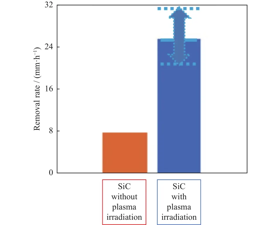
Fig.7 Comparison of removal rate of SiC substrate with and without plasma irradiation
3 Enhancement of surface oxidation during CMP
3.1 Chamber-type CMP equipment that can be controlled by the processing environment
To accelerate the processing of hard-to-process substrates, it is necessary to form an oxide-like film type product on the extreme surface.From various methods, we focused on the processing environment and considered an apparatus that can perform CMP by sealing the entire CMP device with a pressure container and confining various high-pressure gases.Figure 8 shows the concept of an atmosphere-controlled CMP.A photograph of the prototype chamber-type CMP apparatus that was manufactured and an internal structure diagram are shown in Figure 9.The chamber that was made of stainless steel can be mixed with gas up to 1 MPa using a gauge pressure and it can also be in a vacuum state.Because there are two windows made of quartz in the upper part of the chamber, light rays such as UV irradiation can be incidentally added from there[26].
Figure 10 shows the rate of increase of the GaN substrate (Ga surface side) removal rate when the pressure inside the chamber was increased to 500 kPa by the addition of oxygen gas.As shown in this figure, the removal rate of the GaN substrate was increased by more than 50% by enclosing the high-pressure oxygen gas.Similarly, the removal rate also increased when processing the SiC substrate (see Fig.10).In both cases, the processing progressed with the formation of oxide-like film reaction products on the processed extreme surface playing a major role[27].

Fig.1 Comparison of processing time of each substrate (SiC, GaN, and diamond), assuming that processing conditions of Si were applied

Fig.10 Rate of increase in GaN substrate (Ga surface side)removal rate
Therefore, to increase the thickness of the oxide film on the extreme surface by photocatalytic reaction, the processing characteristics of the CMP under normal atmospheric pressure (i.e., CMP in the case of the open chamber) were compared to the CMP in a high-pressure oxygen / air atmosphere inside the chamber.In each atmospheric gas environment, CMP was performed while irradiating the slurry containing a small amount (0.5 wt%) of fine titanium oxide particles with UV irradiation.Figure 11 shows an example ofCMP of a SiC substrate (Si surface side) under an atmosphere of high-pressure air and oxygen gas (500 kPa).When irradiated with UV, the photocatalytic effect of the ultrafine particles of titanium oxide mixed with colloidal silica had a significantly higher removal rate under high-pressure air or oxygen gas atmosphere than that under CMP with normal atmospheric pressure.In particular, when UV irradiation was added in a high-pressure oxygen atmosphere of 500 kPa, the removal rate was 4 or more times higher than that of the ordinary CMP.Although this is not clearly understood, this was probably because the life of OH radicals generated by the photocatalytic reaction became longer under the highpressure oxygen atmosphere[28].

Fig.8 Proposal of chamber-type controlled atmosphere CMP method and machine-Concept of atmosphere-controlled CMP

Fig.9 Photograph of prototype chamber-type CMP apparatus and internal structure diagram
Consequently, by forming an OH radical field on the processed extreme surface, when a soft reaction product is formed on the extreme surface, the processing of the hard-toprocess material can be achieved.However, for the processing of diamond crystals, which are much more chemically and mechanically stable than SiC and GaN substrates, it is not so easy.Therefore, a new plasma fusion CMP method was devised as a processing method that also introduced a physical processing method.
3.2 Plasma fusion CMP equipment incorporating CMP and P-CVM
To realize highly-efficient processing of hard-to-process materials such as diamonds, it is necessary to consider new processing methods without being prepossessed with the conventional processing / CMP methods.The authors contrived a unique planarization processing method while forming a pseudo-radical field (similar to an ultra-micro damaged layer on the extreme surface) on the extreme surface by polishing / CMP, as well as a highly-efficient isotropic P-CVM under atmospheric pressure[29].This created a combined effect by simultaneously fusing the processing principles of CMP, which is good at smoothing and planarization and P-CVM, which is good at high-efficiency machining although isotropic etching.

Fig.11 Example of CMP of SiC substrate (Si surface side) under atmosphere of high-pressure air and oxygen gas(pressure inside chamber: 500 kPa)
Figure 12 shows an example of the developed plasma fusion CMP system (prototype), which is a structural schematic diagram showing the processing principle and an external photograph.In this system, the machining tool contains a CMP pad and many micro-plasma electrodes that act on PCVM simultaneously.To allow the CMP to flow the processing slurry, the micro-plasma electrode was placed approximately 300 μm lower than the pad surface so that it did not touch the slurry and the reactive carrier gas was added to the upper side[30].This was devised as a special micro-plasma electrode structure.When performing P-CVM alone at an atmospheric pressure using this micro-plasma electrode, the gap between the microelectrode tip and the substrate (several 10 μm to several 100 μm), input power / frequency, and reactive gas species / flow rate were optimized.Most materials can be isotopically etched with high efficiency.The plasma fusion CMP method that was devised formed appropriate pseudo-radical sites / ultra-micro defect field[31]by the physical action of the CMP pad and the fine abrasives in the slurry and preferentially removed the convex portion of it by the P-CVM.Consequently, the processing principles of smoothing and planarization were efficiently performed sim-ultaneously by the fusion effects of CMP and P-CVM.
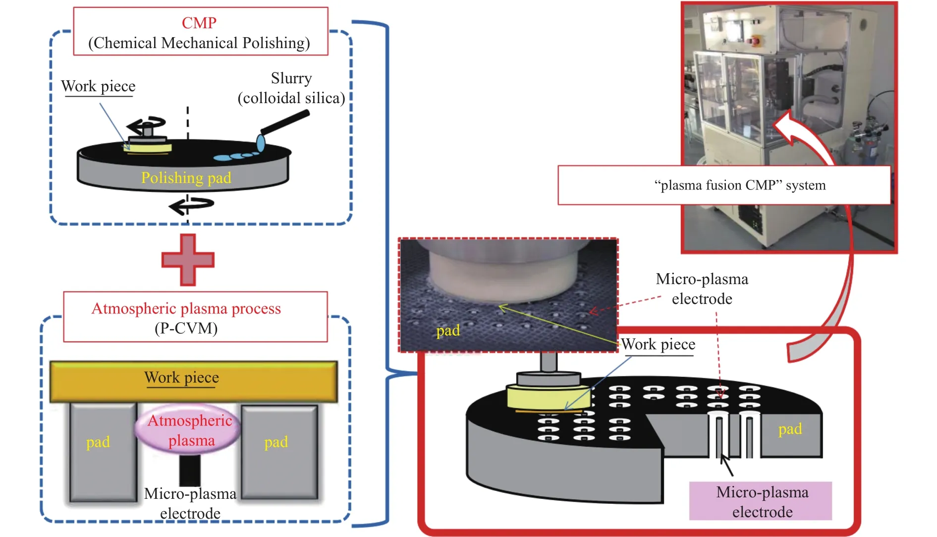
Fig.12 Concept and structural schematic diagram showing the processing principle of plasma fusion CMP system(top right photo: plasma fusion CMP system)
Figure 13 shows an example of the processing characteristics of a plasma fusion CMP for a diamond substrate as well as for SiC and GaN substrates.Regarding the removal rates of CMP alone processing and P-CVM alone processing for each substrate material, the removal rate by plasma fusion CMP is not a simple sum of CMP and P-CVM, although the dominant processing method differs for each material.In other words, it can be understood that there is a synergistic effect of plasma fusion CMP[32].For example, in the case of diamond substrate, the removal rate was extremely low at 1.9 nm/h for CMP alone; however, a very high processing rate of 670 nm/h was obtained for the plasma fusion CMP that performed P-CVM and CMP simultaneously.Such a difference is also in the reduction rate of the surface roughness (Ra) of the processed surface (i.e., the effect of improving the surface roughness within a unit time).Figure 14 compares the surface roughness (Ra) reduction ratio after each substrate of GaN, SiC and diamond for 1 h.From this figure,it is clear that there is a synergistic effect due to plasma fusion CMP, although the reduction rate of surface roughness differs depending on the type of substrate material.
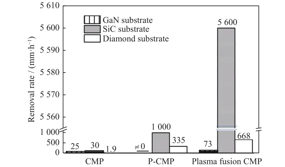
Fig.13 Plasma fusion CMP characteristics of various substrates(removal rate of GaN, SiC and diamond for CMP, P-CVM, and plasma fusion CMP)
In the P-CVM alone of a diamond substrate when O2was used as the reaction gas, both the removal and improvement rates of the surface roughness were higher than those of the SF6gas and the oxygen plasma was more suitable for diamond processing[33].An example of the relationship between the removal rate and supplied power/reactive gases (O2and SF6) in the P-CVM of the diamond is shown in Figure 15.Because it was confirmed as suitable, the processing conditions with O2gas must be optimized in future studies.
Here, the processing mechanism of plasma fusion CMP of a diamond substrate when oxygen gas is applied as the reactive gas is considered as follows.Outwardly, the reactionon the diamond substrate surface is
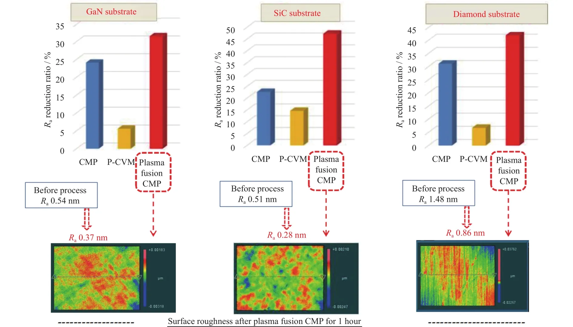
Fig.14 Relationship between surface roughness (Ra) reduction ratio and processing methods (CMP only, P-CVM only and plasma fusion CMP) after each substrate of GaN, SiC and diamond for 1 h
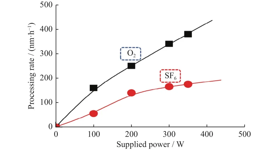
Fig.15 Relationship between processing rate and supplied power/reactive gases (O2, SF6) in P-CVM of diamond

However, in the case of normal plasma, since the temperature of plasma is extremely high (1 000 ℃ to several thousand degrees)[34], this reaction can occur directly.On the other hand, in the case of P-CVM performed under atmospheric pressure, it is assumed that it does not change to CO or CO2because it is a low-temperature plasma (for example,200 ℃ or less)[35]and is within the range of glow- discharge(that is not arc-discharge).At present, it is speculated that a pseudo-radical field due to plasma action is formed on the extreme surface, which is modified into a soft transition reaction product (e.g.Estimated to be CxOyaccording to XPS analysis)[36], which creates a situation that can be easily removed by CMP action[37].Furthermore, unlike P-CVM alone under normal atmospheric pressure, for the plasma fusion CMP, the micro-plasma electrode was lowered by several hundred microns[38].Therefore, the plasma processing was executed in a closed space instead of the normal P-CVM, so that the P-CVM was efficiently advanced.This was similar to the enclosed chamber-type CMP performed in the highpressure gas atmosphere described in the previous section.
From these results, it has been demonstrated that the plasma fusion CMP method that was developed by incorporating the advantages of the planarization performance of CMP and the high-efficiency etching processing of P-CVM into the processing characteristics was highly efficient and produced high-quality processing even for diamond substrates.
3.3 Proposal of next-generation machining process for hard and brittle materials based on machining mechanism
Aiming at effective CMP of various hard and brittle materials, while focusing on the influence of the environment of the processing equipment, we have understood the effects of photocatalytic reaction assistance in a high-pressure oxygen atmosphere, plasma irradiation assistance, and the processing mechanism has been considered.As a result, it is expected that the processing is promoted while forming reaction products such as hydrated film and oxide film on the extreme surface of the processed material.Especially, CMP for photocatalytic reaction assisted by UV irradiation[39]under the environment of high pressure oxygen and plasma-assisted CMP are effective for high efficiency machining.As for a new high-efficiency machining process, it is assumed that the point is to create a situation that facilitates processing by forming a pseudo radical field or reaction product on the extreme surface layer of the processed material[40].
Here, assuming the introduction of the magnetorheological finishing method with a large surface contact tool[41],which is attracting attention as ultra-precision machining, the following will propose an ultra-precision machining process for hard-to-process materials / hard-brittle materials.Figure 16 is an example of an ultra-precision machining process devised.The first step is to form a pseudo radical field / reaction product on the extreme-surface by laser irradiation, UV irradiation, or plasma irradiation in order to make it easier to process the processing part of the difficult-to-process material[42].Then, the second step is to remove the formed pseudo radical field / reaction product by magnetorheological finishing[43].Since the layer formed on the extreme-surface is not so deep, it is assumed that the first step and the second step are repeated, so-called "cyclic processing method".The pseudo radical field in the first step may be formed by applying an idea incorporating an interesting idea of "skin effect"proposed by Zhanget alat SUSTech[44].
Regarding the above, it has already been confirmed that high-efficiency machining is possible by the assumed cyclic machining process, including basic machining principles for the first and second processes.Detailed processing character-istics regarding processing characteristics are currently under consideration and will be reported separately.

Fig.16 Ultra-precision machining process for high-efficiency machining of next generation hard and brittle materials(Eample of proposal for future work based on the mechanism in this research)
4 Summary
To find breakthroughs in high-efficiency and high-quality processing technology for crystal substrates such as SiC,GaN, and diamond as next-generation wide-band-gap semiconductors, two types of CMP processing apparatuses that introduced completely new concepts were manufactured in the present study: a closed chamber-type machining environment control CMP apparatus and a plasma fusion CMP apparatus assisted plasma machining (P-CVM).In the former case, high-efficiency processing by UV irradiation was included to introduce a photocatalytic reaction in a high-pressure oxygen atmosphere.In the latter case, the apparatus was designed especially for the diamond substrate that has the highest hardness on Earth.By applying these apparatuses, the processing mechanisms were investigated, as well as understanding the processing characteristics of hard-to-process materials, as follows:
(1) Considering the processing mechanism from the processing characteristics of various materials that are mechanically or chemically stable, the processing was promoted while forming a hydrated film or soft oxide-like film on the extreme surface during CMP.
(2) The removal rates of the GaN and SiC substrates increased when CMP was undertaken by pressurizing inside the chamber with oxygen gas to 500 kPa using the chambertype CMP apparatus.The removal rate was 2.5 to 2 times higher than that of the normal CMP performed under atmospheric pressure, although it varied depending on the processing conditions.
(3) The removal rate increased when the CMP of the SiC substrate was performed while irradiating UV rays to colloidal silica, although there were differences depending on the processing conditions of including titanium oxide fine particles (0.5 wt%).Due to the photocatalytic effect, the removal rate increased by 20% in the case without UV irradiation.In particular, when UV irradiation was performed in a high-pressure oxygen atmosphere, the photocatalytic reaction was remarkable and the removal rate was approximately 4 times higher than when the ordinary CMP was applied.This is probably because the life of the OH radicals became longer in the high-pressure oxygen atmosphere.
(4) According to the basic processing characteristics of SiC and GaN substrates as well as diamond substrates processed using the plasma fusion CMP apparatus, there was a synergistic effect from combining the plasma processing (PCVM) and CMP.In particular, for the diamond substrate processing, the plasma fusion CMP achieved a very high processing rate of 670 nm/h compared with the removal rate of PCVM or CMP alone.It was also confirmed that the improvement rate of the surface roughness was high.
(5) The processing of the diamond substrate in the plasma fusion CMP was based on the expected reaction on the surface of the diamond substrate by the plasma:

Therefore, the soft intermediate reaction product layer generated when changing to CO or CO2was preferentially removed by CMP.Furthermore, it was assumed that the locally enclosed space between the pad surface and processed substrate was similar to the chamber-type CMP apparatus and became the high-density plasma processing state to facilitate processing.
(6) Based on the studied processing mechanism, a "cyclic processing method" consisting of two steps, a pseudo radical field / reaction product formation step and a magnetorheological finishing step, was proposed as a highly efficient processing process.
Acknowledgments
We would like to thank everyone involved in this joint research enterprise, including Kyushu University, Saitama University, and Osaka University, for helping to conduct a part of this research.We would also like to express our sincere gratitude to Fujikoshi Machine Industry for their cooperation in the production of the equipment.
