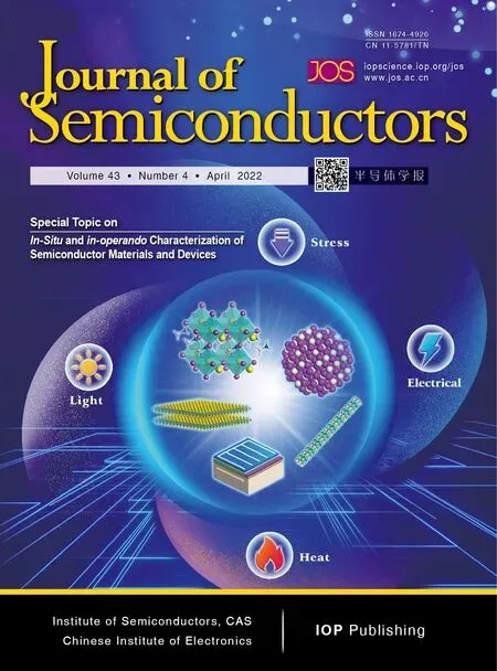
Preface to the Special Topic on In-Situ and in-operando Characterization of Semiconductor Materials and Devices
2023-01-05XiaoxingKeandYongZhang
Xiaoxing Ke and Yong Zhang
1Faculty of Materials and Manufacturing, Beijing University of Technology, Beijing 100124, China
2Electrical and Computer Engineering Department, University of North Carolina at Charlotte, Charlotte, NC 28223, USA
Characterization of materials and devices is fundamental to the understanding of structure-property relationship and improving device performance. Driven by the rapid progress achieved in semiconductors research, advanced characterization techniques at high spatial resolution are being developed, with the capability to reveal microstructures down to atomic or sub-atomic scale. Coupled within-situandin-operandotechniques, responses of materials and devices under multiple external stimuli can be investigated at both high spatial resolution and high time resolution, providing in-depth understanding of the growth, reaction, defects evolution and degradation mechanism etc. with unprecedented details.
This special issue assembles 6 review articles providing a timely summary of advancedin-situandin-operandocharacterization techniques, covering areas of traditional semiconductor devices, organic semiconductor devices, metal oxide semiconductors, photocatalysts, and halide perovskites.
Jianget al.dedicate the review to the up-to-date developments in thein-situ/operandooptical, scanning probe microscopy, and spectroscopy techniques specifically for organic semiconducting films and devices[1]. Simultaneous probes of film morphological evolution, crystal structures, semiconductor-electrolyte interface properties, and charge carrier dynamics, as revealed by advancedin-situ/operandocharacterization, effectively facilitate the exploration of the intrinsic structure-property relationship of organic materials and the optimization of organic devices for advanced applications.
Zhanget al.introduce a comprehensive approach of defect study, i.e., a series mode, to address the issues of traditional parallel mode where defects investigated by structural characterization techniques were not the same defect that affected the device[2]. As demonstrated by thein-operandostudy of individual dislocation type defects in GaAs solar cells, this novel approach is able to offer answers to questions like: (i) how do individual defects affect device performance? (ii) how does the impact depend on the device operation conditions? (iii) how does the impact vary from one defect to another?
Liet al.deliverer a comprehensive review on quantitative transmission electron microscopy (TEM) characterization where off-axis electron holography is introduced in detail[3].This unique method is illustrated by applications in various semiconductor nanomaterials including group IV, compound and two-dimensional semiconductor nanostructures, both in static states and under various stimuli. Particularly, the challenges facing thein-situelectron holographic study of semiconductor devices at working conditions are presented.
Fanget al.summarize the recent progress ofin-situcharacterization techniques on exploring the dynamic behavior of catalyst materials and reaction intermediates[4]. Semiconductor photocatalytic processes revealed by microscopic imaging and spectroscopic characterization are discussed. Challenges inin-situcharacterization are highlighted, geared toward the development of more advancedin-situtechniques to guide the design of advanced photocatalysts.
Zhaoet al.review the recent progress regarding the mechanical deformation mechanisms in metal oxide semiconductors, such as CuO and ZnO nanowires (NWs), usingin-situTEM[5]. Enabled byin-situmechanical testing, the phase transformation of CuO NWs under compressive stress and phase transition in ZnO NWs under tensile strain is revealed down to atomic scale.
Wuet al.provide a timely review on recent studies of the halide perovskites using advanced TEM characterization[6].Due to the extreme beam-sensitivity of the halide perovskites, the irradiation damages caused by the interaction between the electron beam and perovskite sample under the imaging conditions are discussed in detail. Emerging TEM techniques such as cryo-TEM, ptychography etc. are then discussed, where recent achievements on atomic-resolution imaging, defects identification and chemical mapping on halide perovskites are reviewed. Particularly, the developments ofin-situTEM in the degradation study of the perovskites under different environmental conditions such as heating, biasing, light illumination, and humidity are reviewed.
We sincerely hope this special issue could provide timely review and perspective on the development of emerginginsitu/operandocharacterization techniques and their contributions to unveil the structure-property relationship in semiconductor materials and devices, and ultimately improve the device performance. We also hope this special issue could not only benefit the on-going research in lab and industry by introducing cutting-edge characterization techniques, but also inspire more creative approaches to be developed for semiconductors research in the coming future.
We would like to thank all the authors for their outstanding contributions to this special issue. We are also grateful to the editorial and production staff of theJournal of Semicon-ductorsfor their kind assistance.
杂志排行
Journal of Semiconductors的其它文章
- Stabilizing α-phase FAPbI3 solar cells
- Janus VXY monolayers with tunable large Berry curvature
- DASP: Defect and Dopant ab-initio Simulation Package
- Recent progress on advanced transmission electron microscopy characterization for halide perovskite semiconductors
- Structural evolution of low-dimensional metal oxide semiconductors under external stress
- In-situ monitoring of dynamic behavior of catalyst materials and reaction intermediates in semiconductor catalytic processes
