In-situ monitoring of dynamic behavior of catalyst materials and reaction intermediates in semiconductor catalytic processes
2022-04-26ZhenFangYaoLiuChengyiSongPengTaoWenShangTaoDengXiaoqinZengandJianboWu
Zhen Fang , Yao Liu , Chengyi Song Peng Tao Wen Shang Tao Deng Xiaoqin Zeng , and Jianbo Wu
1State Key Laboratory of Metal Matrix Composites, School of Materials Science and Engineering, Shanghai Jiao Tong University,Shanghai 200240, China
2Center of Hydrogen Science, Shanghai Jiao Tong University, Shanghai 200240, China
3National Engineering Research Center of Light Alloy Net Forming, Shanghai Jiao Tong University, Shanghai 200240, China
4Materials Genome Initiative Center, Shanghai Jiao Tong University, Shanghai 200240, China
5Future Material Innovation Center, Zhangjiang Institute for Advanced Study, Shanghai Jiao Tong University, Shanghai 200240, China
Abstract: Semiconductor photocatalysis, as a key part of solar energy utilization, has far-reaching implications for industrial, agricultural, and commercial development. Lack of understanding of the catalyst evolution and the reaction mechanism is a critical obstacle for designing efficient and stable photocatalysts. This review summarizes the recent progress of in-situ exploring the dynamic behavior of catalyst materials and reaction intermediates. Semiconductor photocatalytic processes and two major classes of in-situ techniques that include microscopic imaging and spectroscopic characterization are presented. Finally, problems and challenges in in-situ characterization are proposed, geared toward developing more advanced in-situ techniques and monitoring more accurate and realistic reaction processes, to guide designing advanced photocatalysts.
Key words: in-situ; semiconductor photocatalyst; materials evolution; reaction intermediate
1.Introduction
With the climate issues caused by the rapid development of industry and the energy demand brought by the increase in population, people face the problems of energy shortage and global warming. The development of semiconductor photocatalysts has realized these important reaction processes[1−3], including hydrogen evolution reaction, oxygen evolution reaction, CO2conversion, and N2fixation,which rely on abundant solar resources. It is of great significance for producing and collecting green hydrogen energy,the production of high value-added chemicals, batteries, nitrogen fertilizer, pollutant treatment, and other commercial and agricultural fields.
At present, semiconductor catalysts have received extensive attention and rapid development because of their green and pollution-free catalytic process and the effective catalytic ability for slow and complex kinetic processes. Nevertheless, there are still some obstacles. For example, photogenerated carriers are difficult to excite, have a high recombination rate and low transfer efficiency, and have low reaction activity on the catalytic surface. To solve these problems,researchers have proposed strategies such as heterojunction engineering[4−7], defect engineering[8], morphology regulation[9−11], element doping[12], and cocatalyst loading[9,13]to design efficient, low-cost and large-scale semiconductor photocatalysts.
However, most of these studies focus on the changes of materials before and after the reaction, and the changes in the reaction process are not clear, which is of great significance to improve the stability of the catalyst. Therefore, it is necessary to further reveal the dynamic changes of materials and the changes of reaction intermediates at the surface and interface using in-situ or operando characterization methods and equipment, including microscopic imaging and spectral characterization (Fig. 1).
2.Semiconducting photocatalysis and in-situ characterization techniques
2.1.Principle of photocatalysis
The semiconductor is a kind of material with a unique energy band structure whose conductivity is between the conductor and insulator at room temperature. The special energy band structure of semiconductors consists of the valence band, conduction band, bandgap, and Fermi level(Fig. 2)[14]. Based on the presence or absence of impurities,semiconductors can be divided into intrinsic type, negativetype, and positive-type, respectively (Figs. 2(a)–2(c)). Generally, the energy band structure and electron distribution are different in different types of semiconductors.
A classical semiconductor photocatalytic process will undergo three critical processes (Fig. 2(d)): first, light absorption excites electron–hole pairs; second, the separation of photogenerated electron holes and transfer to the surface and interface of catalyst; third, the occurrence of reduction or oxidation half-reaction at the surface and interface of catalyst. In the photocatalytic process, some critical aspects need to be paid attention to. First, the semiconductor catalysts need to have a suitable energy band structure, including bandgap and energy level. A suitable energy gap can combine high carrier separation efficiency with excellent photocatalytic activity. Semiconductors with energy levels higher than redox potential are more conducive to photocatalytic reaction specifically, the low solar absorption caused by the wide bandgap is not favorable for separating electron–hole pairs. However,the narrow bandgap will produce electrons or holes with low reduction or oxidation potential, resulting in low photocatalytic activity. Therefore, bandgap and activity are two seemingly contradictory. Second, semiconductor catalysts need to have effective separation of photogenerated carriers and efficient surface transport to improve the activity and speed of photocatalytic reaction. Third, the catalysts need to have a relatively stable thermodynamic phase to improve the stability in the reaction processes[15], but this seems to be contrary to the high surface reaction activity. At present, semiconductor heterojunction engineering and defect engineering are considered to be effective measures to solve the existing problems.

Fig. 1. (Color online) In-situ characterization of semiconducting photocatalysts for material research and mechanism disclosure in solar energy conversion and the storage process.
In the process of the photocatalytic reaction, the catalyst material evolution will occur, such as atom migration andinsitushelling, and a series of reaction intermediates will appear at the surface and interface of the catalyst. These evolutions have an important impact on the activity and stability of the catalytic reaction and the elaboration of the deeper reaction mechanism. Therefore, it needs to be characterized by matchingin-situtechniques[15].
2.2.Characterization techniques to support and demonstrate
Modern advanced characterization techniques have been applied in the study of catalysts[16]. As shown in Fig. 3, when high-energy stimuli meet materials, materials will feedback various signals, and specific signal collectors can be used to obtain relevant material structure information. Photon rays and electron beams are the most common stimulus. After stimulating, the feedback signals include photon or electron diffraction signal, photon attenuation signal, electron energy signal,and so on. There are varieties of devices for collecting information, generally can be divided into two common technologies. One is spectroscopic technology, in which the change of physical properties and chemical composition of materials can be studied according to the spectroscopic signal absorbed or emitted by the material[17]. The other is microscopic imaging technology, which provides visible images of morphology and structure[18]. The principle of several advanced characterization methods in photocatalysts is introduced below in combination with Fig. 3 and helps us understand the applications.
X-ray photoelectron spectroscopy (XPS) is a comparatively surface-sensitive (about 10 nm depth) technology[19].The principle of XPS is using X-rays to irradiate samples and result in the photoelectric effect (Fig. 3). Inner electrons or valence electrons of atoms or molecules are excited by photons and are named photoelectrons. The binding energy of photoelectrons can be measured and is specific to elements. Defects in catalysts can alter the electrical structure and chemical environment of the elements, resulting in spectrum variations such as peak shift, intensity fluctuation, or the formation of additional peaks[20]. In addition, changes in element-binding energy can accurately represent changes in electron density. As a result, binding energy changes can be utilized to analyze the direction of charge carrier transfer in heterojunction photocatalysts[21].
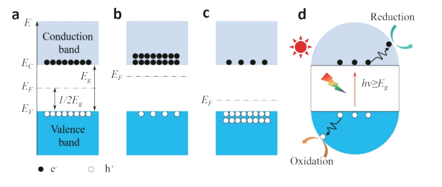
Fig. 2. (Color online) Energy band diagram and electron distribution of three typical types of semiconductors, including (a) intrinsic type, (b) negative-type, and (c) positive-type. (d) Mechanism displays of semiconductor photocatalysis.
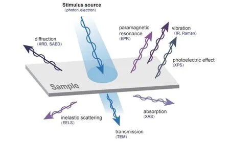
Fig. 3. (Color online) Schematic diagram of the interaction between particles (electrons and photons) and materials.
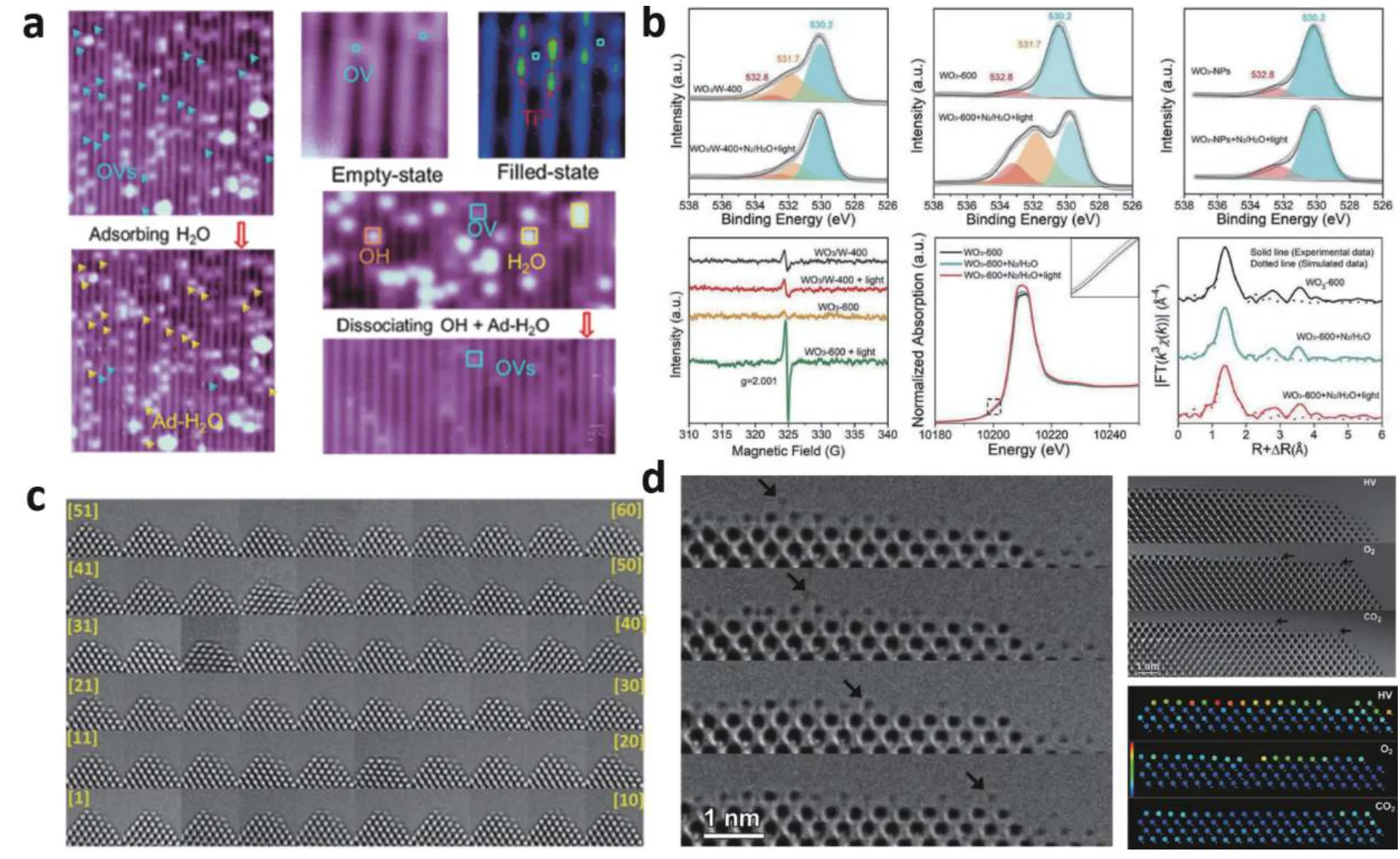
Fig. 4. (Color online) (a) In-situ STM observation of oxygen vacancies dynamic changes on TiO2(110) surface. (b) In-situ XPS, in-situ EPR, in-situ XAS (XANES) and in-situ EXAFS spectra in R space of WO3-600. (c) Series of in-situ TEM images of a CeO2 nanoparticle. (d) In-situ TEM images of atom mobility on CeO2 surface at {100} facet in high vacuum, oxygen, and carbon dioxide atmospheres. Modified with permission from (a) Ref.[32] Copyright 2018 American Chemical Society, (b) Ref. [33] Copyright 2019 WILEY-VCH Verlag GmbH & Co. KGaA, (c) Ref. [35] Copyright 2017 American Chemical Society, (d) Ref. [36] Copyright 2011 WILEY-VCH Verlag GmbH & Co. KGaA.
X-ray absorption spectroscopy (XAS) characterizes the material by measuring the absorption coefficient of X-ray[22]. The intensity of an X-ray is attenuated when it travels through a substance. If the incident X-ray energy is too low, the orbital electrons in the element are not excited. When the energy of the X-rays is strong enough to excite core electrons to the unoccupied state, the X-ray is significantly absorbed, resulting in a dramatic jump in the spectrum known as the X-ray absorption near edge structure (XANES). This part can be used to identify particular elements and is sensitive to the oxidization state. The core electrons stimulated to a continuous state create outgoing and scattering wave interference with nearby atoms as X-ray energy rises. Extended X-ray absorption fine structure (EXAFS) formed in this region reflects local atomic structures including bond distance and coordination number.
Infrared (IR) spectroscopies use infrared light to stimulate materials and probes dipole moment changes by the vibrations and rotations of bonds in molecules, functional groups,and radicals[23]. Although IR is not surface sensitive, it can discern the difference between free molecules and adsorbates bonded to solid surfaces in any environment due to small changes in vibrational frequencies.
Raman spectroscopy is another useful vibrational spectroscopy. This technique utilizes a visible light laser for excitation and measures the energy losses between incident photons and inelastically scattered photons, acquiring polarizability change in a sample under vibrational modes. Raman is very adept at identifying low-frequency modes, which are difficult to detect by traditional methods[24]. Sometimes Raman spectroscopy and IR spectroscopy can complement each other. Normal Raman signals are not enough inaccurate tracking of reaction, but surface-enhanced Raman spectroscopy(SERS) can help to solve it and show great potential inin-situcatalytic studies[25].
Electron paramagnetic resonance spectroscopy (EPR),also known as electron spin resonance (ESR), is a magnetic resonance technology to directly detect and study unpaired electron paramagnetic[26]. It is often used to detect single-electron capture vacancy defects in materials with high sensitivity. For example, if a material contains unpaired electrons, it will be subjected to an applied magnetic field. When this magnetic field is applied, the unpaired electrons in the material will align in a certain orientation, and Zeeman splitting will occur. The strength of the magnetic field is proportional. If electromagnetic waves with the same energy difference as the Zeeman split level are added to the vertical magnetic field direction, resonance occurs. The information of defect type and relative concentration was obtained according toGvalue and signal strength.
A transmission electron microscope (TEM) is commonly employed for direct observation of nanomaterials[27]. A highenergy electron beam is incident into a quite thin TEM sample, and the electrons elastic collide with the atoms in the material and change direction. The scattering angle is related to the sample's density and thickness, allowing the formation of various bright and dark pictures that will be magnified and focused on the imaging equipment. When equipped with a spherical aberration corrector, atomic resolution images can be achieved. Electron energy loss spectrum (EELS)and electron diffraction are auxiliary functions of the electron microscope and provide some extra information about material composition and structure[28]. EELS characterize the elemental composition, chemical bonding, and electronic structure of materials by detecting energy loss of incident electrons, which is caused by an inelastic collision between transmission electron and sample electron. In addition, when satisfying Bragg's equation, elastic electrons can form a diffraction pattern on the dorsal focal plane in diffraction mode and provide crystal structure information of materials. Selectedarea electron diffraction (SAED) can analyze some specific microregions with an objective aperture. Scanning transmission electron microscopy (STEM) is another important imaging technology of electron microscope and is a clever combination of SEM and TEM. It uses a high-energy electron beam to scan thin samples, and the annular detector collects the high angle scattered electrons to image. STEM resolution has reached atomic scale, andZcontrast (whereZrepresents the atomic number of the atom) imaging can be obtained in STEM mode. In addition, the development of a dedicated environmental transmission electron microscope (ETEM) plus the modified TEM sample holders, which allow for the presence of either gas or liquid and makein-situstudies in TEM possible.In-situTEM or STEM characterization of the photocatalytic process can be carried out after the introduction of light irradiation.
A scanning tunneling microscope (STM) uses the quantum tunnel effect to identify the atomic arrangement on the material's surface by measuring the tunneling current between the probe tip and the material surface[29]. After processing the tunnel current, the intuitive 3D surface image can be obtained. STM serves the following functions: identification of the surface structure, analysis of surface defects as well as investigation of adsorbate adsorption and dissociation behavior. Since the working environment of STM is not demanding,in-situSTM studies can monitor surface alteration of the photocatalyst during adsorption and reaction processes under liquid and atmosphere.
Scanning electrochemical microscopy (SECM) works on electrochemical principles and measures the electrochemical currents given by the oxidation or reduction of substances within a microzone, which is ideal for exploring the heterogeneous catalysis process considering that it combines the spatial resolution of scanned probe microscopy with thein-situmanipulation of electrochemical techniques[30]. The approach scans and obtains the associated micro-area electrochemistry and related information using extremely small electrodes (probes) driven close to the sample, which can be a conductor, insulator, or semiconductor.
3.Evolution of catalytic materials
3.1.Single-component semiconductors
When a single-component semiconductor is employed as a photocatalytic model, all charge-kinetics processes stated above can occur on the same semiconductor catalyst. As a result, their photocatalytic active surface change is relatively simple, including some defect dynamics and surface structural evolution. This part mainly introduces some examples of usingin-situtechnologies to monitor the evolution in single-component semiconductor catalysts and aids in the insight into the mechanism.
Defects play a crucial role in photocatalytic reactions since they are highly connected with the surface-active site[8].For example, one of the most typical defects in metal–oxide–semiconductors is oxygen vacancy. The introduction of oxygen vacancy makes the metal atoms of metal oxides present an unsaturated coordination state and provides an effective channel for the transfer of electrons from the semiconductor to the adsorbed gas molecules[31]. Oxygen vacancies were found to change dynamically during photocatalysis in many studies. Fig. 4(a) shows a work clarifying the catalytic kinetics of oxygen vacancy on TiO2(110) surface byin-situSTM[32]. In this study, oxygen vacancies are the major structural defects on the surface of the TiO2(110) single crystal. Before reaction, the adsorbed H2O molecules are located at the oxygen vacancy site; with the catalytic reaction, the surface oxygen vacancy is repaired, while the second layer oxygen vacancy can exist stably. It indicates that some catalytic reactions take place at the cost of oxygen vacancy consumption.Besides, other experiments have found thatoperandooxygen vacancies can also be created in the catalytic process[33].The defect evolution was monitored in real-time usingin-situXPS, ESR, and XAS during the N2reduction process (Fig. 4(b)).Quasiin-situXPS was performed before and after treating a flowing H2O vapor of N2with light for 30 min. Before the reaction, there was no indication ofoperandooxygen vacancies in WO3-600, but after exposure to N2and H2O under light irradiation, there was a significant signal foroperandooxygen vacancies emerging. The generation ofoperandooxygen vacancies in WO3-600 under catalytic condition was further verified byin-situESR and XAS.
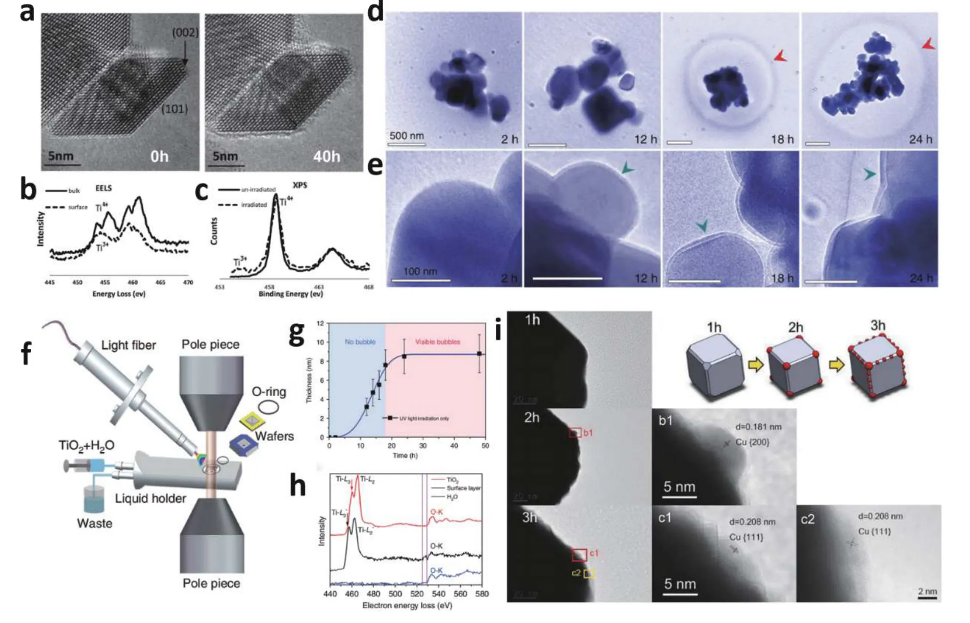
Fig. 5. (Color online) (a) In-situ TEM images of TiO2 under water vapor conditions, with (b) EELS spectra and (c) XPS spectra of TiO2 particles. Insitu TEM study of TiO2 photocatalytic water splitting under UV light: (d) formation and evolution of bubbles, (e) magnified views of the surface shell on TiO2, (f) schematic diagrams of fluidic TEM holder with in-situ UV illumination, (g) surface shell thickness on TiO2 under UV illumination and (h) EELS spectra of the TiO2. (i) HRTEM images of Cu2O samples irradiated for 1, 2, and 3 h, as well as schematic diagrams of Cu2O structure change during irradiation. Modified with permission from (a), (b) and (c) Ref. [38] Copyright 2013 American Chemical Society, (d), (e), (f), (g) and(h) Ref. [39] Copyright 2018 Springer Nature, (i) Ref. [40] Copyright 2020 Elsevier Ltd.
Surface atom migration on specific facets of semiconductors often occurs under photocatalytic reactions, which may influence their catalysis and stability. Some works report that the inelastic scattering of electron beam in electron microscopy can bring about an effect similar to that of UV light[34].While electron beam irradiation would be absent as a stimulant in real-world circumstances, the paths of atomic surface rearrangements are likely to be similar. It is of indirect relevance to applications in photocatalysis. The Ce atom migration has been studied by using anin-situaberration-corrected transmission electron microscopy (AC-TEM), and 60 TEM images of the {100} facet at the CeO2nanoparticle corner were shown in Fig. 4(c)[35]. Atomic hopping activities were discovered reversible. On this basis, the mobility of Ce atoms at{100} facet in different atmospheres was characterized by anin-situETEM (Fig. 4(d))[36]. When under a high vacuum, Ce atoms were observed to change rapidly from one frame to the next. Under O2ambient circumstances, the (001) surface is now ended by oxygen columns, which inhibit the mobility of the Ce atoms. Furthermore, when CO2is injected into the chamber, surface mobility is entirely stopped.
With the advancement ofin-situTEM, it is possible to directly observe the chemical change process of catalyst surface during light irradiation rather than electron beam irradiation mentioned above[37]. Then understand the change of surface structure and active site in the real photocatalytic process. In addition, EELS or XPS can be adopted to prove the chemical composition of the material at each stage of the photocatalytic process. Crozieret al. used the ETEM to study TiO2nanoparticle surfaces in a true photocatalytic reaction with high-intensity broadband light and water vapor conditions[38]. The surface of TiO2was smooth and well crystalline when light and water vapor were first introduced, but then the surface became coarse and covered by a disordered TiO2amorphous layer after 40 h of reaction (Fig. 5(a)). The amorphous layer showed very stable under further irradiation. The state of the Ti species was examined using EELS and XPS to determine the amorphous phase's composition (Figs. 5(b) and 5(c)), revealing that part of the surface layer was reduced to the Ti3+state while the bulk stayed in the Ti4+.
Since most characterizations for photocatalytic reactions of anatase TiO2are limited to water vapor environment, Suiet al. established a novel method to examine photocatalytic water splitting using anatase TiO2in a genuine reaction environment (Fig. 5(f))[39]. The photocatalytic reactions reported in water differ significantly from those observed in vapor. A shell layer formed on the surface of TiO2nanoparticles in the aqueous phase as the reaction proceeded, and bubbles formed around the TiO2nanoparticles subsequently (Figs.5(d) and 5(e)). Fig. 5(d) shows the growth rate of the shell on TiO2and found it has a maximum thickness of around 8.8 nm. The components of the shells were studied with the use of EELS. In Fig. 5(h), the EELS data implies that Ti in the surface shell has a lower valence state. Authors proposed that hydrogen atoms will preferentially enter into the interior of TiO2lattice, leading to the transformation of Ti4+to Ti3+in the low state and then forming a nanoscale hydrogenation shell on the surface of TiO2.
Yuet al. also obtainedin-situTEM observations of an unstable Cu2O catalyst during a photocatalytic reaction. Fig. 5(i)shows HRTEM images of Cu2O samples in continuous irradiation[40]. Within 1 h of light, the Cu2O cubes had barely changed. After 2 h of exposure to light, the surface of Cu2O became increasingly rough, and Cu particles initially formed in the corner. Cu on Cu2O surface strewn from the corner to the edge of Cu2O cubes when the illumination continued to 3 h.In this work, selected area electron diffraction (SAED) and other reduction experiments are used to further verify the generation of Cu. Finally, formed nano-Cu was verified to be the photocatalytic reaction's active site.
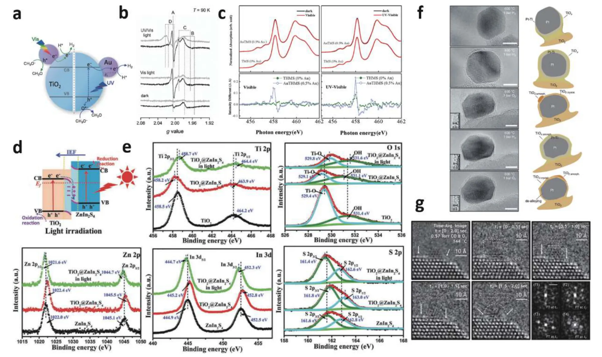
Fig. 6. (Color online) (a) Schematic diagram of water reduction in Au-TiO2 with UV- (right) and visible-light (left) driven. (b) In-situ EPR spectra of TiO2 and Au-TiO2. (c) In-situ XAS spectra of THMSs and Au THMSs. (d) Schematic illustration of the electron transfer mechanism between TiO2/Zn-In2S4 S-scheme heterojunction. (e) In-situ XPS spectra of TiO2, ZnIn2S4, and TiO2/ZnIn2S4. (f) In-situ TEM observations about evolution and dynamic structural changes of the overlayer in a strong metal-support interaction. (g) Time-series in-situ ETEM image of Pt-loaded CeO2. Modified with permission from (a) and (b) Ref. [43] Copyright 2013 Wiley-VCH Verlag GmbH & Co. KGaA, (c) Ref. [44] Copyright 2018 American Chemical Society, (d) and (e) Ref. [52] Copyright 2021 Wiley-VCH GmbH, (f) Ref. [53] Copyright 2021 Springer Nature, (g) Ref. [54] Copyright 2020 Springer Nature.
3.2.Multi-component semiconductor
To promote the photocatalytic efficiency of semiconductors, various studies forward from the single-component system to the multi-component hybrid system, like a metal–semiconductor hybrid, semiconductor–semiconductor hybrid, and so on[14]. Charge creation and consumption may occur simultaneously on separate components in multi-component semiconductors, and charge transfer is usually done from one component to another. Furthermore, additional interfaces between the various components can be active reaction sites and alter dynamically during reactions. In a word, with the improvement of catalyst performance, both charge kinetics and structure change become more complicated. This section will provide some applications ofin-situcharacterization of multicomponent semiconductor photocatalysts.
Integration with metal can harness the charging kinetics of semiconductors. Especially some noble metals, such as Au,Ag, and Cu, which offer strong plasmonic properties, can improve the activity of semiconductors[41]. For example, TiO2has a wide bandgap and can only convert UV light into chemical energy. Au-loaded TiO2not only shows an improved activity in UV light than pristine TiO2. And Au-loaded also brings an imparting strong visible-light photo absorption capability to TiO2(Fig. 6(a))[42]. The application ofin-situspectroscopy can provide a piece of reliable evidence on charge transfer mechanisms between metal and semiconductor under reaction conditions. Priebeet al. use anin-situEPR to monitor water reduction over Au-TiO2catalysts. As shown in Fig. 6(b)[43],signal A is formed in Au-loaded TiO2irradiated with visible light. In contrast, no signal in pure TiO2. Signal A reflects trapped electrons from Au nanoparticles, demonstrating that electrons driven by visible-light transfer from the Au to the TiO2surface, and are trapped by vacancies at the Au-TiO2interphase. Another work usesin-situXAS to monitor Auloaded TiO2hollow microspheres under visible-light illumination (Fig. 6(c)), also find the signal to prove that hot electron charge transfers due to surface plasmon resonance effect from Au 5d to Ti 3d t2g[44].
Construction of heterojunctions in semiconductor–semiconductor photocatalysts is another way to steer the charging kinetics, such as extending the spectral range for light absorption and enhancing electron-hole separation[45,46]. For instance, oxidation photocatalyst (OP) with low VB and low CB position displays strong oxidation ability but relatively low activity. Conversely, reduction photocatalysts (RP) stand out for their high CB position and large driving force for running the photocatalytic reduction reaction. Since various semiconductor materials have characteristic band structures, different combinations of semiconductor materials will form different junctions[4,47−49]. The experimental requirement for demonstrating charge carrier transfer on heterojunction has always been a tough process[50,51]. Anin-situXPS technique was used by Yuet al. to confirm a step-scheme (S-scheme) heterojunction mechanism on TiO2/ZnIn2S4for photocatalytic CO2reduction[52]. The schematic illustration andin-situXPS are shown in Figs. 6(d) and 6(e). When TiO2/ZnIn2S4is in darkness, the binding energies of O 1s and Ti 2p shift to lower energy levels, and binding energies of Zn 2p, In 3d, and S 2p shift to higher energy levels, implying that the electrons transfer from ZnIn2S4to TiO2. After light irradiation, the binding energies shift reversely, suggesting the photo-generated electrons transfer from TiO2to ZnIn2S4under light irradiation.
For multi-component semiconductors, the interfacial alterations of multiple components are also significant in the catalytic process. Many atomic-scale evolutions of the metal particle, oxide surface, and interface during catalysis remain unanswered.In-situTEM is the best method to visualize atomicscale dynamics. When there is a strong metal-support interaction (SMSI), metal nanoparticles can be reversibly covered when the support undergoes reduction. Bokhovenet al., use anin-situTEM to study an actual Pt/TiO2catalyst under changing gas atmosphere (Fig. 6(f))[53]. Pt develops a covering on its surface when exposed to hydrogen, and EELS mapping indicates that these species are Ti-containing. The overlayer abruptly increased after changing the gas environment to oxygen. When the gas environment was shifted back to hydrogen, dynamic changes occurred in the overlayer. And the overlayer decreased in thickness. As the interfacial energy undulates during the catalytic process, significant variation in metal particle form and bonding occurs, and the metal particle's adherence to the support may deteriorate. Crozieret al. employin-situAC-TEM to study the structural dynamics occurring at and near Pt/CeO2interfaces during carbon monoxide oxidation[54].In-situETEM images and the Fourier transform(FT) are shown in Fig. 6(g). It can be found that diffuse intensity caused by fluxional dynamics appears at both the Pt nanoparticle and the perimeter of the Pt/CeO2interface.
4.Dynamic process of surface reaction intermediate
Accurate and intuitive observation of the dynamic process of reaction intermediates is helpful to reveal the mechanism of photocatalysis and design an advanced photocatalyst.In-situmonitoring provides an effective tool for detecting reaction intermediates in the whole photocatalytic process[55,56].The reaction intermediates and the intrinsic mechanisms involved in various catalytic processes are different, and herein some important single/multi-electron reaction processes are summarized.
4.1.Water photosplitting including HER and OER
The water-splitting, including hydrogen evolution reaction (HER) and oxygen evolution reaction (OER) (Fig. 7(a)), are key chemical reactions for green hydrogen production and energy conversion process[1,2,57]. The identification of reaction intermediates in the HER and OER processes is of significance for mechanistic understanding[58−63].
To monitor the water-splitting HER mechanism under realistic working conditions, Guoet al. proposed anin-situmeasurement system combining linear-sweep voltammetry curves andoperandoRaman spectra and a possible HER mechanism of MoS2xSe2(1−x)(Figs. 7(b)−7(d)). The spectra results show that H atoms are adsorbed to the active S/Se atoms (or atoms) to form intermediate MoS2-H/MoSe2-H and subsequent hydrogen desorption during the HER process[64].
In addition,in-situdiffuse reflectance infrared Fouriertransform (DRIFT) spectroscopy were performed to determine the possible reaction intermediates on the ZnIn2S4@MoS2in photocatalytic HER[65]. As shown in Fig. 7(e), a series of IR peaks at 3608, 1314, 1265, 1077, 1630, and 3440 cm–1were monitored, in which 3608 cm–1corresponds to the S–H, 1314 and 1265 and 1077 cm–1correspond to the adsorbed O from SOX, 1630 and 3440 cm–1are assigned to the H2O and OH, respectively. With the prolonged irradiation time in the presence of H2O, the height of the peak at 3608 cm–1gradually increased, meaning that the H atom tends to adsorb on S sites.Then the height of the peak at 3440 cm–1is also raised after H adsorption reaches equilibrium. When turning on the Xe lamp, the intensity of peaks at 3608 and 3440 cm–1gradually declined with the illumination time, verifying the activation of S–H and subsequent H2desorption process (Fig. 7(f)). Further, a possible reaction pathway for the HER process over the ZnIn2S4@MoS2with visible-light illumination was proposed in Fig. 7(g).
By analyzing the variations of infrared peaks after illumination within-situFourier-transform infrared (FTIR) technique,Yeet al. studied the process of the HER on ReS2/CdS under different sacrificial reagents, including Na2S-Na2SO3and lactic acid[66]. Specifically, for Na2S-Na2SO3, the spectra result confirmed that H2O will decompose and SO32−will be oxidized to SO42−(Fig. 7(h)). And according to the spectra result, lactic acid will decompose into -OH and -COOH, and then react with H2O to form H2(Fig. 7(i)). Electron paramagnetic resonance (EPR) system was also used to detect the signal intensity of •O2–to prove the direct Z-scheme charge migration mechanism in the Sv-ZIS/MoSe2system as an efficient HER photocatalyst[67].

Fig. 7. (Color online) In-situ characterization of reaction intermediates in the photocatalytic HER and OER processes. (a) Mechanism scheme of HER and OER. (b) LSV curve (left) and (c) operando Raman spectra (right) of MoS0.9Se1.1. (d) Schematic illustration of the HER process in MoS2xSe2(1–x). (e) In-situ DRIFT spectra of H2O on the ZnIn2S4@MoS2 with 2 h H2O-saturated flow under He and (f) with a 2 h irradiation time under Xe lamp, and (g) proposed reaction pathway for the HER process over the ZnIn2S4@MoS2. In-situ FTIR spectra of the HER process on ReS2/CdS with two different sacrificial agents, (h) Na2S-Na2SO3 and (i) lactic acid. Modified with permission from (b), (c) and (d) Ref. [64] Copyright 2020 Wiley-VCH Verlag GmbH & Co. KGaA, (e), (f) and (g) Ref. [65] Copyright 2021 Elsevier Ltd., (h) and (i) Ref. [66] Copyright 2019 Elsevier Ltd.
Primary intermediates of ultraviolet light-induced OER on the TiO2(rutile) particles were monitored within-situMIRIR spectroscopy, and the results support the previously proposed OER mechanism[68]. By using time-resolved rapid-scan FTIR spectroscopy, two reaction intermediates of visible lightsensitized water oxidation on the Co3O4were identified, and different catalytic sites were identified based on the kinetic behavior of the intermediates[69]. For NaTaO3-based photocatalysts, according to thein-situFTIR spectral results, the appearance of two new water oxidation intermediates, corresponding to the 1058 and 935 cm–1peak positions, was thought to be derived from Ta(VI)=O and Ta(O2) peroxo species, respectively[70].
4.2.CO2 conversion
Solar CO2conversion, including CO2photoreduction and CO2photofixation to valuable chemicals (Fig. 8(a)), play an important role in energy storage and global warming[71−76]. The evolution of intermediates and possible reaction mechanisms based on different CO2conversion reactions are summarized[77−79].
Based on defect engineering, Wuet al. designed a kind of BiOBr layers with enriching oxygen vacancies and adoptedin-situFTIR spectroscopy to monitor the reaction intermediates during CO2photoreduction to CO[80]. With the increase of radiation time, seven IR absorption peaks gradually appear (Fig. 8(b)). Among them, the two IR peaks at 1550 and 1200 cm–1are derived from the COOH*, which verify that the COOH* are reaction intermediates. Further, a possible pathway for CO2photoreduction has been proposed (Fig. 8(c)):the CO2adsorption and H2O dissociation occur simultaneously, and the adsorbed CO2* interacts with the surface protons to produce COOH*, and further protonation of COOH*to generate the CO*.
Chenet al. explored that the important role of oxygen vacancy confined in Bi2O3nanosheets in the conversion process of CO2and elaborated the reaction mechanism of CO2photofixation to long-chain chemicals byin-situDRIFT spectroscopy[81]. As shown in Fig. 8(d), after irradiation of the OVrich-Bi2O3nanosheets in the presence of CO2and CH3OH,three new IR peaks at 1294, 1456, and 1779 cm–1appeared,corresponding to •CO2–, CO3= and dimethyl carbonate (DMC),respectively. With the increase of illumination time, it can be seen that the intensity of these peaks gradually increases and the •CO2–tends to stabilize. However, the product of DMC continues to rise. Based on the monitored intermediates, a reasonable reaction mechanism was proposed as schematically illustrated in Fig. 8(e).
Within-situDRIFT spectroscopy, Wanget al. detected carbon-based species formed on the surface of S-scheme coreshell TiO2@ZnIn2S4heterojunction photocatalyst during photocatalytic CO2reduction reaction (Fig. 8(f))[52]. After light irradiation, several absorption peaks of key reaction intermediates are generated, including COO−, HCHO−, HCOO−and CH3O−, which show that the effective photoreduction process of CO2on the TiO2@ZnIn2S4and reveal a possible CO2conversion pathway (Fig. 8(g)).
The photothermal effect is not emphasized in traditional photocatalytic systems. To reveal the CO2reduction intermediates and to further address the role of photothermal during the photocatalytic reactions,in-situFTIR experiments were conducted at different temperatures with the oxygen vacancyrich Zn2GeO4nanobelts[82]. With the extending light irradiation time, the adsorbed CO2was converted into COOH* and CO* at 298 K (Fig. 8(h)), whereas the photothermal effect induced the coupling of CO* to form OCCO* at 348 K (Fig. 8(i)).Therefore, the C–C coupling step can be achieved by the photoinduced heat effect (Fig. 8(j)). In addition,in-situFTIR spectral was used to prove that the COOH is the critical reaction intermediate in the process of CO2photoreduction to CO and CH4on the BiOX[83].
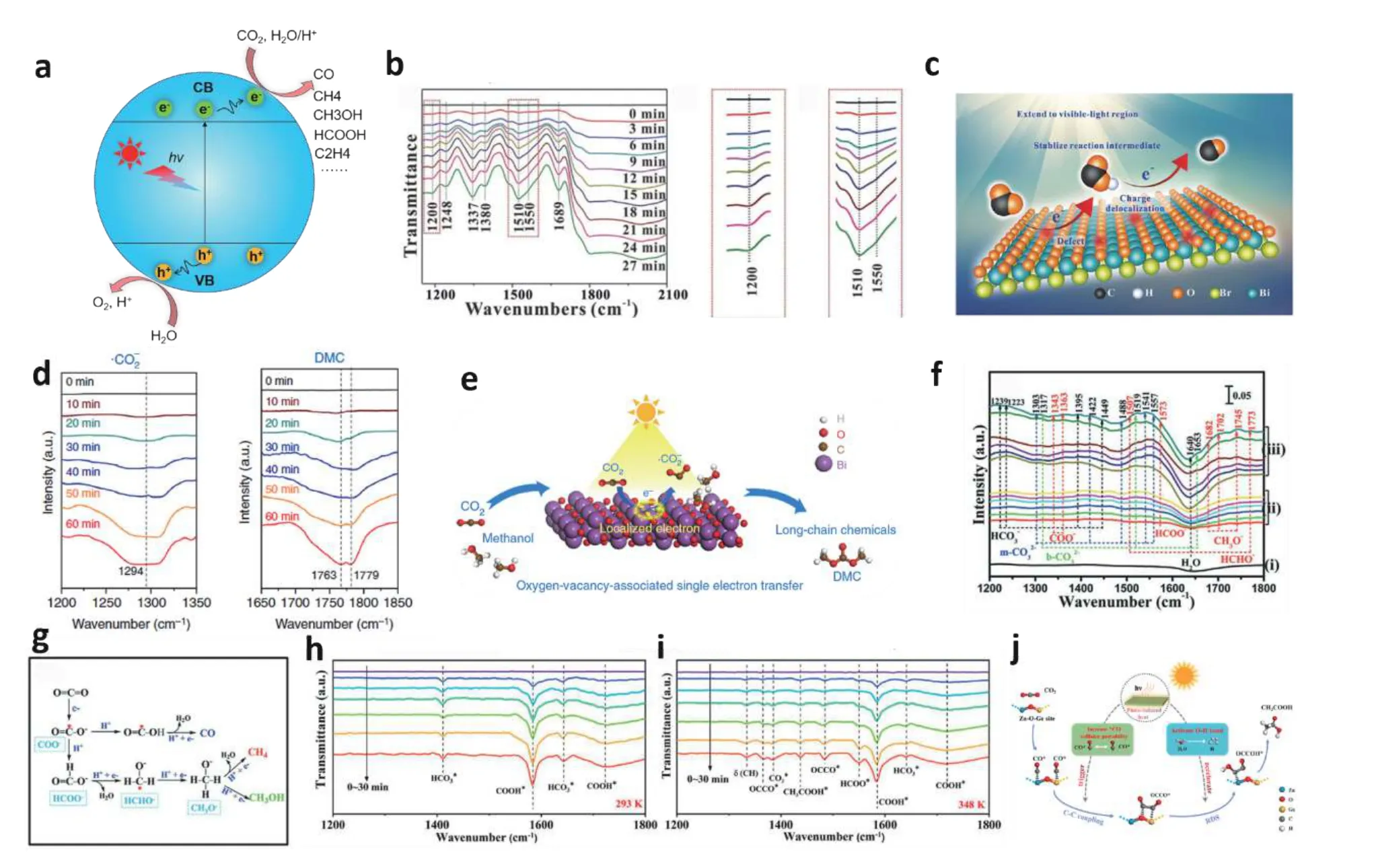
Fig. 8. (Color online) In-situ characterization of reaction intermediates in the photocatalytic CO2 conversion processes. (a) Mechanism scheme of CO2 conversion. (b) In-situ FTIR spectra of CO2 adsorbed on the BiOBr layers with oxygen vacancy in the presence of H2O vapor. (c) Schematic illustration for CO2 photoconversion into CO over the oxygen-vacancy BiOBr. (d) In-situ DRIFTS spectra for the conversion process of CO2 in the presence of CH3OH under Xe lamp for oxygen vacancy-rich-Bi2O3 nanosheets. (e) Schematic illustration for CO2 photofixation to long-chain chemicals. (f) In-situ DRIFTS spectra of CO2 reduction reaction and (g) possible photocatalytic pathways over the TiO2@ZnIn2S4. In-situ FTIR spectra of atmospheric 0.03 vol % CO2/Ar photothermal reduction over the oxygen vacancy-rich Zn2GeO4 nanobelts at (h) 293 K and (i) 348 K. (j) Function mechanism of photoinduced heat during CO2 photoreduction to CH3COOH. Modified with permission from (b) and (c) Ref. [80] Copyright 2021 Wiley-VCH GmbH, (d) and (e) Ref. [81] Copyright 2019 Springer Nature, (f) and (g) Ref. [52] Copyright 2018 Wiley-VCH Verlag GmbH & Co. KGaA,(h), (i) and (j) Ref. [82] Copyright 2021 American Chemical Society.
4.3.N2 fixation
Ammonia, an important raw material for nitrogen fertilizer, is synthesized from N2and H2under high temperature and pressure using the Haber–Bosch process[84]. To address energy and environmental issue, a photocatalytic nitrogen fixation strategy with atmospheric pressure and ambient temperature was proposed (Fig. 9(a))[3,85−87]. The evolution of intermediates and possible reaction mechanisms based on photocatalytic nitrogen fixation reactions are summarized[88−96].
Liet al. developed a simple low-temperature synthesis method to obtain a series of Bi5O7Br nanostructures[94]. The nitrogen photofixation reaction dynamics were detected by anin-situIR system with a synchrotron radiation light source.InsituIR spectra of Bi5O7Br-40 (40 °C of thermal treatment temperature) show that the intensity of several IR peaks changes with adsorption and irradiation time. Peak i to peak vi are assigned to N–H (3555 cm−1), -OH (3360 cm−1), NH4+(2874 cm−1), CO2(2359 cm−1), N2(1624 cm−1) and NH3(1557 cm−1),respectively. (Fig. 9(b) and 9(d)). Upon visible light (Fig. 9(c)),the intensity of peaks i, iii, and iv decreases, while the intensity of peaks ii, v, and vi increases, which indicates the enhanced process of N2adsorption, activation, and N–H conversion to NH3(Fig. 9(c)). By comparing Fig. 9(a) and Fig. 9(d),the intensity of peaks i and iii increases, while the intensity of peak v decreases, indicating the effective breakage of the N≡N triple bond and the production of NH4+. By comparing Fig. 9(c) and Fig. 9(e), the intensities of peaks i and ii remain unchanged after turning off the light source while the intensities of peaks iii, iv, and vi increase, suggesting that an increase in N-H concentration and N2adsorption. These spectra results reveal that the preparative adsorption of N2on the Bi5O7Br-40 may be responsible for its outstanding N2photofixation performance.
Wanget al. utilizedin-situDRIFT spectroscopy to investigate the evolution of N-related intermediates in the early stages on the Bi5O7Br-NT[95]. With the increase of irradiation time, several IR bands gradually increased (Fig. 9(f)), where 3555 & 1713 & 1667 cm−1, 1403 & 2874 cm−1, 1713 & 1557 cm−1, and 1624 cm−1are assigned to N–H, NH4+, NH3and N2,respectively. The spectra show that the intensity of N≡N will continuously decrease in the form of OV–N≡N and N≡N will breakage to NH3or NH4+. Therefore, the N2photofixation mechanism over the Bi5O7Br-NT could be proposed as shown in Fig. 9(g).
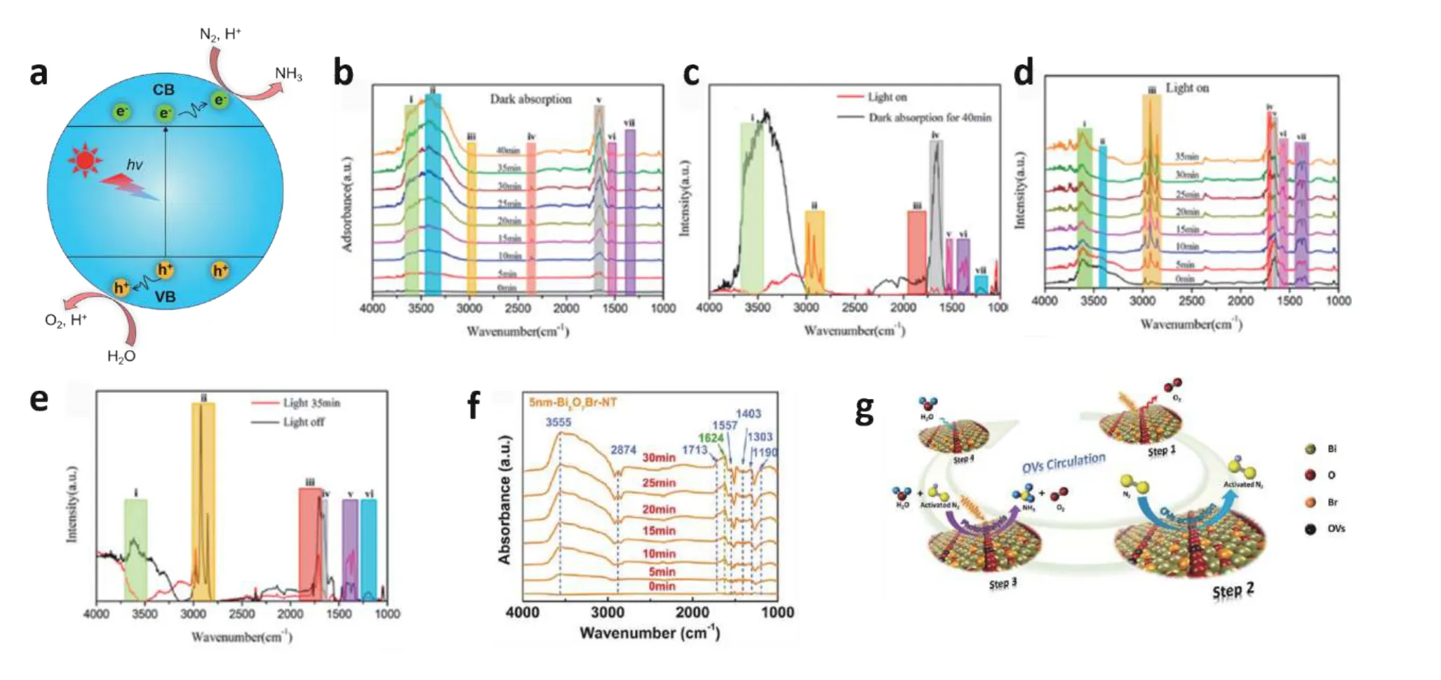
Fig. 9. (Color online) In-situ characterization of reaction intermediates in the N2 photofixation process. (a) Mechanism scheme of N2 fixation. Insitu IR spectra of Bi5O7Br-40 in the process of (b) N2 adsorption from 0 to 40 min in the dark, (c) afterward receive visible light illumination, (d)then visible light illumination lasts 35 min, and (e) finally the visible light illumination is turned off. (f) In-situ DRFTIRS spectra were obtained and(g) a reaction pathway of N2 photofixation over the Bi5O7Br nanotubes. Modified with permission from (b), (c), (d) and (e) Ref. [94] Copyright 2020 American Chemical Society, (f) and (g) Ref. [95] Copyright 2020 American Chemical Society.
To directly observe the mechanistic process of N2photoreduction, Liet al. usedin-situDRIFT spectroscopy to monitor the evolution channel of reaction intermediates on the BiOBr within a well-designed reaction cell[93]. As for BOB-001-OV with {001} facet-exposed, several IR signals gradually increased with the extension of irradiation time in the N2atmosphere, but no obvious signal appears on the BOB-001-H (reference photocatalyst without OVs). The spectra result verified that the significance of OVs on the N2photofixation on the BiOBr.
4.4.Other catalytic processes
In addition to the above catalytic process, some other critical reactions[97−100], such as NO removal, oxygen reduction reaction (ORR), are also proposed here.
NO from industrial emissions is considered an important contributor to air pollution and has adverse effects on human health[101]. The selective and effective removal of NO by a photocatalyst is an environment-friendly and cost-efficient way, compared with the traditional treatment method of high temperature and pressure[102,103].
Shanget al. designed a kind of oxygen vacancy rich-blue TiO2photocatalyst for highly selective removal of NO and proved the reaction mechanism of selective NO removal[98].As shown in Figs. 10(a) and 10(b), with the extension of lighting time, the increased absorption peaks of 1700–1100 cm−1could be assigned to monodentate (1326 and 1282 cm−1)and bidentate (1607, 1460, 1120, 1577, and 1469 cm−1) nitrates over the TiO2-OV and TiO2. In contrast, increased new peaks at 1690 and 1142 cm–1were confirmed for NO+and NO2–over the TiO2(Fig. 10(b)). The comparative spectra result between TiO2-OV and TiO2prove that the photogenerated holes are the cause of NO2production. Thus, the mechanism of selective NO removal was demonstrated (Fig. 10(c)).
In addition, thein-situFTIR spectra were used to analyze the time-dependent NO oxidation process in the presence of Bi0OVs-(BiO)2CO3[97]. Several IR peaks representing nitrogen species appear with the extending irradiation time, which reveals the existence of multiple NO oxidation pathways (Fig.10(d)). Therefore, the reaction mechanisms of three possible NO removal pathways over Bi0OVs-(BiO)2CO3were proposed(Fig. 10(e)).
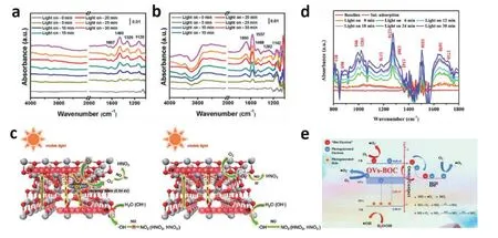
Fig. 10. (Color online) In-situ characterization of reaction intermediates in other catalytic processes. In-situ FTIR spectra of (a) TiO2-OV and (b)TiO2. (c) Selective removal mechanism during the NO removal process over the TiO2-OV and TiO2. (d) In-situ FTIR spectra and (e) NO removal mechanism of Bi0OVs-(BiO)2CO3. Modified with permission from (a), (b) and (c) Ref. [98] Copyright 2019 American Chemical Society, (d) and (e) Ref. [97]Copyright 2019 Elsevier Ltd.
Adsorbed hydroxyl radical •OH(ads)is an important surface immediate for photocatalysis reaction of TiO2[56]. Surface interrogation-scanning electrochemical microscopy (SISECM), a means of local monitoring of materials that combine high resolution and composition detection, is used for studying the dynamic behavior of •OH(ads)on a TiO2substrate electrode with nano-size structure[100]. A typical SISECM operation mode is made up of three steps: pre-processing of the SI-SECM system under the dark condition and a negative feedback tip current will be observed for the first step; generation of •OH(ads)under light irradiation and subsequently a time decay of •OH(ads)in the dark and no tip current will be displayed for the second step; interrogation of•OH(ads)in the dark and a transient positive feedback tip current will be observed for the final step. Surface intermediates of photocatalytic oxygen reduction reaction (ORR) on the TiO2films in aqueous solutions were directly detected within-situFTIR for the first time and a possible reaction mechanism was proposed[104].
5.Conclusion and prospects
Despite these advances in the field ofin-situcharacterization of photocatalysis, there is still an urgent need to further develop advanced and robust techniques to track the evolution of materials and reaction intermediates to gain a deeper understanding of the material changes and reaction mechanisms in the process of photocatalytic reactions.
Forin-situspectroscopic characterization, it is necessary to accurately control the reaction temperature, pressure, and atmosphere, and reduce the influence of the reaction device,so as to realizein-situmonitoring under real reaction conditions. Therefore, rational design of thein-situdevice is required, for example, using more accurate probing thermocouples as close to the reaction system as possible without affecting the reaction environment. Use inert materials to design the reaction device to avoid the impact on the reaction environment at high temperatures. In addition, transient spectroscopy techniques with higher temporal resolution should be emphasized to monitor the kinetic behavior of active sites and reaction intermediates.
For microscopic imaging technology, especiallyin-situTEM, the pursuit of high resolution (including spatial resolution and time resolution) is an eternal topic. Since catalysis reactions often occur at breakneck speed, time resolution needs to be improved with a good image signal-to-noise ratio to capture the dynamics and identify more intermediates in catalysis reactions. The advancement of electron detection can be quite beneficial. Like the newly developed approach allows for the detection of a single electron without the need to convert it to photons. Thein-situTEM can be utilized to examine dynamics on a millisecond time scale with this feature.The ultrafast TEM uses a brief electron pulse with a high current density and has a time resolution of up to femtoseconds.Ultrafast electron diffraction, in particular, can be used to investigate catalytic reactions with a significantly better temporal resolution.
Meanwhile,in-situTEM needs to strike a balance between radiation damage and image resolution. Radiation damage is mainly caused by high-energy electron beams.When a sample is not resistant to radiation, the greatest defense is to lower the energy of the electron beams. The electron beam can be reduced while keeping acceptable resolution using spherical aberration-corrected electron microscopy. Note that when EDS and EELS are adopted, samples must be exposed to relatively high-energy electrons. It can be considered to carry out EDS and EELS analysis after the imaging characterization, which can reduce the generation of false images and improve the accuracy of experiments. In addition, updating the reaction cell materials to increase chip mechanical strength and chemical resistance would result in reduced window bulging, reducing the thickness of the liquid or gas layer, and so boosting spatial resolution.
Finally, thein-situcharacterization process should organically combine a variety ofin-situtechniques, including spectroscopy, microscopic imaging, and performance monitoring systems, to achieve a comprehensive and multidimensional information tracking of catalyst materials and reaction intermediates during the photocatalytic reaction. In addition, it is also necessary to focus on the whole photocatalytic process from beginning to end to elaborate on the real reaction mechanism and provide a deeper perspective on the design of advanced catalysts.
Acknowledgements
The work was supported by the National Science Foundation of China (21875137, 51521004, and 51420105009), Innovation Program of Shanghai Municipal Education Commission(Project No. 2019-01-07-00-02-E00069), the 111 Project(Project No. B16032), and the fund from Center of Hydrogen Science and Joint Research Center for Clean Energy Materials at Shanghai Jiao Tong University for financial supports.
杂志排行

Journal of Semiconductors的其它文章
- Stabilizing α-phase FAPbI3 solar cells
- Preface to the Special Topic on In-Situ and in-operando Characterization of Semiconductor Materials and Devices
- Janus VXY monolayers with tunable large Berry curvature
- DASP: Defect and Dopant ab-initio Simulation Package
- Recent progress on advanced transmission electron microscopy characterization for halide perovskite semiconductors
- Structural evolution of low-dimensional metal oxide semiconductors under external stress