Structural evolution of low-dimensional metal oxide semiconductors under external stress
2022-04-26PeiliZhaoLeiLiGuoxujiaChenXiaoxiGuanYingZhangWeiweiMengLigongZhaoKaixuanLiRenhuiJiangShuangfengJiaHeZhengandJianboWang
Peili Zhao , Lei Li , Guoxujia Chen Xiaoxi Guan Ying Zhang Weiwei Meng Ligong ZhaoKaixuan Li Renhui Jiang Shuangfeng Jia He Zheng , and Jianbo Wang
1School of Physics and Technology, Center for Electron Microscopy, MOE Key Laboratory of Artificial Micro- and Nano-structures,and Institute for Advanced Studies, Wuhan University, Wuhan 430072, China
2Suzhou Institute of Wuhan University, Suzhou 215123, China
3Wuhan University Shenzhen Research Institute, Shenzhen 518057, China
Abstract: Metal oxide semiconductors (MOSs) are attractive candidates as functional parts and connections in nanodevices.Upon spatial dimensionality reduction, the ubiquitous strain encountered in physical reality may result in structural instability and thus degrade the performance of MOS. Hence, the basic insight into the structural evolutions of low-dimensional MOS is a prerequisite for extensive applications, which unfortunately remains largely unexplored. Herein, we review the recent progress regarding the mechanical deformation mechanisms in MOSs, such as CuO and ZnO nanowires (NWs). We report the phase transformation of CuO NWs resulting from oxygen vacancy migration under compressive stress and the tensile strain-induced phase transition in ZnO NWs. Moreover, the influence of electron beam irradiation on interpreting the mechanical behaviors is discussed.
Key words: metal oxide semiconductor; phase transition; strain; nanowire; in-situ transmission electron microscopy
1.Introduction
Modern technological pressure to develop miniature electronic devices with improved performance has led to the rapid expansion of research into low-dimensional metal oxide semiconductors (MOSs), which have been extensively applied in thin film transistors[1], flat panel displays[2], logical gates[3], biosensing[4], gas sensors[5−7], smart windows[8,9],and so on. MOS nanomaterials can also serve as nano-level interconnects and active components in optoelectronic devices and nano-electro-mechanical systems (NEMS)[5,10]. Success in these endeavors requires a set of correlated design principles, based on correlating the structural features to the functions. While considerable efforts have been spent to investigate the electrical, optical, and chemical properties[11−14], the mechanical properties of MOSs subjected to the ubiquitous strain in nanodevices have been overlooked. The mechanical strain can induce elastic or plastic deformation, which inevitably affects the electronic structures and thus the functions of MOSs[15−18]. For example, the elastic strain can be applied to effectively tune the band gap width of TiO2, thereby improving its photocatalytic efficiency[19−21]. Hence, the fundamental understanding of mechanical behaviors is of great significance in view of the property-oriented structural design.
Generally, due to the limitations of size and the quantity of defects, nanosized MOSs (e.g., ZnO, CuO, Nb2O5, and WO3,etc.) can sustain a larger strain of ~3%−10% compared with their bulk counterparts[22−25]. Experimental studies have shown that the maximum strain of ZnO nanowires (NWs) increases from 1.7% (corresponding to stress ~2.4 GPa) to 7.8%(~13.2 GPa) when the lateral size decreases from 760 to 100 nm[26]. Likewise, bulk CuO is inherently brittle. As the size decreases, the CuO NWs exhibit high stress-related bending capabilities[27]. In addition, Lim et al.[28]and Wang et al.[29]reported the diameter-dependent variation in Young’s modulus which could be attributed to density variation defects in Nb2O5and WO3NWs.
Nonetheless, most of the experimental researches have focused on the macroscopic mechanical properties within the elastic range; while knowledge regarding the microscopic deformation mechanisms, especially the defect dynamics is far less developed. Due to the experimental limitation in manipulating the nanosized materials, studies regarding defect evolutions under mechanical stress heavily rely on the theoretical predictions, whereas the interatomic potentials, idealized crystal structure, and ultra-high strain rate may affect the simulated results[30,31]. In recent years, following the development of high spatial resolution transmission electron microscopy (TEM) and NEMS, in-situ TEM[32−37]provides an ideal platform for probing the atomic-scale evolutions of low-dimensional materials under mechanical strain[38−41]. For semiconductors, Huang et al.[42]reported the dislocation dynamics in the GaN NWs. Zhao et al.[43]captured unit cell-by-unit cell latticetrapped cracking in ReS2nanomaterials. However, regarding MOSs, the presence of light element oxygen makes the atomic-scale investigation of deformation mechanisms more challenging using TEM because the high-energy electron beam(e-beam) inevitably induces structural damage. Hence, caution must be taken when interpreting the mechanical behaviors of MOSs inside the TEM. In addition, the deformation behaviors of MOSs are different from those of metals, which show much larger plasticity induced by the various kinds of defect activities. For instance, ZnO nanowires fractured when the strain was 6.5%[44], while BCC metal Nb NW exhibited a superior plastic deformation with a remarkable elongation of more than 269% before fractured[45].
This review focuses on the recent progresses regarding the microscopic deformation mechanisms in CuO and ZnO NWs. Based on the direct evidence of atomistic phase transition processes induced by the mechanical stresses, the deformation mechanisms are unveiled by applying both firstprinciples calculations and molecular dynamics (MD) simulations. The e-beam irradiation effects on low-dimensional MOS are then discussed. Finally, some future perspectives oninsitunanomechanical researches in low-dimensional MOS are given.
2.In-situ nano-mechanics in low-dimensional MOS
Mechanical deformations in crystalline materials are contributed by the recoverable elastic strain (i.e., the lattice expansion/contraction), followed by the irrecoverable plastic strain(i.e., the lattice distortion), which is represented by the nucleation and movement of different types of defects[46,47]. Metal oxides are generally considered to be brittle materials,which fracture with limited plasticity when subjected to mechanical stress. Hence, extensive research efforts have focused on the elastic deformation in MOSs[27,48−51]. However, the defects have been intentionally introduced during the sample synthesis to effectively tune the electrical and optical properties in low-dimensional MOSs[52,53]. In physical reality, the ubiquitous strain/stress in MOS-based MEMS systems may induce the mechanical deformation in MOSs. Hence, it is necessary to unveil the defect behaviors under the external strain,which will constitute a key advance in controlling the properties of MOS.
There are three major kinds of defect structures reported in the MOSs. The first are planar defects, such as stacking faults (SFs) or twinning. SF or twinning deformations have been widely applied to enhance the strength and plasticity of metals and alloy[54−57]. Recently, Thillyet al.[58]reported enhanced plasticity due to the deformation twins in InSb semiconductor. Zhuet al.[59]revealed that the elastic modulus of GaN NWs depended on the relative orientations and the volume fractions of the planar defects. However, for MOS nanomaterials, the SF and twins are mainly introduced during the sample growth rather than by the mechanical stress[60].Second are line defects, such as full dislocations. For semiconductors, full dislocations nucleation, motion, and interaction could contribute for the ultra-large straining ability[31,61]. Unfortunately, little is known regarding the full dislocation dynamics in MOSs, whereas the growth process could inevitable introduce the full dislocations[62]. Third are point defects, such as the oxygen vacancy. Oxygen vacancy is an intrinsic defect in MOS, which is often mobile and highly diluted. This makes it difficult to detect these defects inside TEM. Shanet al.[63]showed that oxygen vacancies could strongly influence the mechanical properties of ZnO NWs by using photo-luminescence spectrum (ex-situ). Sinnottet al.[64]predicted that oxygen vacancies might lead to a ~20% decrease in the Young’s modulus for [0001]-oriented Al2O3nanomaterials. In addition,point defects migration might be limited in bulk materials at room temperature, yielding a negligible effect on the mechanical behaviors according to the Gorsky effect[65−67]. Recently,it was shown that the high stress in single-crystalline ZnO NWs subjected to the compression may facilitate the fast (migration rate ~1.9 × 10⁻¹⁴cm2/s) and reversible migration of oxygen vacancies, and thus result in the anelastic strain[68].However, suffering from the difficulty in resolving point defects, direct evidence is not available to certify the conclusion especially when point defects are mobile under external stress. By compressing single-crystalline CuO NWs (Fig. 1(a)),we reported the nucleation of oxygen-deficient CuO0.67phase transition induced by the migration of oxygen vacancies from tensile to compressive side due to the stress gradient along the NW axial direction (Fig. 1(b)). After the stress was released, the NW underwent an instantaneous elastic strain recovery followed by a much slower (up to tens of minutes) strain recovery, which is a characteristic anelastic behavior (Fig. 1(a)), accompanied by the reversible phase transition from CuO0.67to CuO (Fig. 1(c)). This implies the reversible migration of oxygen vacancies.

Fig. 1. (Color online) Anelasticity in CuO induced by the point defects migration[69]. (a) Schematic illustration of the anelastic deformation process. (b) High-resolution TEM (HRTEM) image showing the nucleation of CuO0.67 phase (enclosed area), indicated by the inserted fast Fourier transform (FFT) pattern. (c) The reversible transition from CuO0.67 to CuO after the compressive stress released.
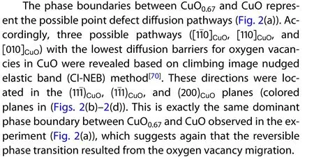
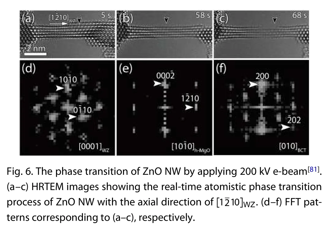
Apart from the defect behaviors, phase transition could be another deformation mechanism related with the plasticity in MOS. For instance, there are three kinds of structures in bulk ZnO–wurtzite (WZ), zinc blende (ZB), and rock salt(RS) structures[71], which could be effectively tuned by changing the growth conditions[35,62]. By decreasing the size down to its exciton Bohr radius (~2 nm), Freemanet al.[72]and Morgan[73]predicted the mechanical strain-induced phase transition of ZnO film from WZ to graphite-like (h-MgO) or body-centered tetragonal (BCT) structure due to the quantum confinement effect[74−77]. In sharp contrast, even though the graphite-like structure was found in ultrathin ZnO films grown on metal substrates, such as Au, Pd, Pt, etc.[78−80],only brittle fractures were observed in ZnO NWs with diameters down to 20 nm according to the tensile loading experiments[44,48]. This discrepancy could be rationalized by the different lateral sizes investigated in theoretical models (~2 nm)and experiments (~tens of nm). To address this gap, we have fabricated the quantum confined ZnO NWs (diameter ~2 nm)via top-down method inside TEM[81]. Subsequently, the phase transition from WZ (Fig. 3(a)) to intermediate BCT and finally h-MgO structures (Fig. 3(b)) was directly observed under tensile stain. Additionally, the h-MgO structure transformed back to the BCT configuration (Fig. 3(c)) before the NW fractured. The averaged strain for initiating the phase transition along thedirection is estimated to be ~3.5%. The reversed phase transition occurred after the NW fractured.
To clarify the underlying phase transition mechanisms,the surface and bulk energies of the NW with WZ, h-MgO,and BCT structures (Fig. 4(a)) under different tensile strains were calculated. A phase diagram related to the width and thickness of the NW, under 0% and 7% strain is presented in Fig. 4(b). The results elucidate that both the sample morphology and strain play important roles in mediating the phase stability of ZnO, which is consistent with the previous reports[82,83].

Fig. 2. (Color online) Oxygen vacancy diffusion pathways in CuO[69]. (a)The high-angle annular dark field (HAADF) showing lattice planes of CuO and metastable CuO0.67 phases. (b –d) Three possible diffusion pathways of O vacancies in CuO. The brown and blue spheres depict O and Cu atoms, respectively.
3.Influence of e-beam irradiation
Although the high-energy electrons inside TEM can provide ultra-high spatial (e.g. sub-Å) and energy resolution for imaging and elemental analysis[84], the e-beam may also cause temporary or permanent changes in solid materials[85].Regarding the low-dimensional MOSs, the electron-matter interactions generally cause detrimental effects through elastic collisions with atomic nuclei and inelastic scattering, which may lead to two major e-beam irradiation effects (i.e. knockon effect and radiolysis)[86]. The knock-on effect implies atomic displacement by e-beam irradiation through elastic scattering, while radiolysis indicates chemical bond breaking through inelastic scattering[87]. Generally, reducing the ebeam energy can alleviate the knock-on damage but simultaneously increase the radiolysis effect in semiconductors. Further decreasing the e-beam intensity may minimize the structural damage induced by radiolysis. Hence, it is advised that caution must be taken to avoid the irradiation-effect induced mis-interpreting of mechanical behaviors.
Here, by taking CuO and ZnO as examples, we show our attempt to minimize the possible irradiation effects on the deformation behaviors. The irradiation effects on the structural changes in CuO and ZnO nanomaterials have been investigated[88,89]. Mechanical tests were then conducted at the conditions with minimized irradiation damage (e.g., lower e-beam intensity and energy). (1) regarding the void migration induced anelasticity in CuO, we have performed the bending tests on the same NW both under “beam-on” (with extremely low beam intensity ~10 A/cm2) (Figs. 5(a)–5(d)) and“beam-off” (Figs. 5(e)–5(h)) conditions. It was found that the NW consistently showed anelasticity with and without continuous e-beam irradiation. However, the continuous irradiation could accelerate the recovery of anelastic strain in CuO (Fig.5(i)). It is speculated that the e-beam could result in the nucleation of oxygen vacancies by knock-on mechanism and provides the energy for vacancy migration, thus contributing to the accelerated strain recovery. (2) ZnO shows an unusual resistance to high-energy e-beam irradiation, whereas the point defects on both Zn and O sub-lattices could rapidly self-annihilate even at low temperature (~130 K)[90−92]. Accordingly, we conducted the tensile tests in ZnO by using both 80 keV with extremely lower intensity (~102A/cm2) (Fig. 3) and 200 keV (current intensity ~103–104A/cm2) (Fig. 6) e-beam[81].The maximum energies that 80 and 200 keV e-beam could transfer to an O atom were 11.8 and 32 eV, respectively. This suggests that the knock-on damage can be alleviated at 80 keV[89]. In addition, the decomposition of ZnO nanoparticles was observed due to radiolysis under the focused e-beam (current density ~3480 A/cm2)[85], which are much higher than those applied in our experiments (~102A/cm2). The current experiments consistently show the same phase transition pathway, as further confirmed by the simulation results. Although the e-beam irradiation was expected to have negligible effects on the phase transition, further studies are required to unveil the phase stabilities of WZ, BCT, and h-MgO ZnO structures under e-beam illumination with decreasing energy and intensity.

Fig. 4. (Color online) The phase stability of WZ, h-MgO, and BCT structures in ZnO[81]. (a) The cross-sectional view of ZnO showing the bond formation and breaking during the phase transition (“○” represents the bond formation of Zn–O, “×” represents the bond breaking of Zn-O). (b) The phase diagram related to the width and thickness of the NWs under 0% and 7% strain. The red and grey spheres depict O and Zn atoms, respectively.

Fig. 5. (Color online) The effects of e-beam irradiation on the anelasticity in CuO NWs[27, 69]. (a–d) TEM images showing the anelastic strain recovery with e-beam illumination. (e–h) TEM images showing the anelastic strain recovery of the same CuO NW without e-beam. The images were taken every 10 seconds. (i) Curves showing the anelastic strain as a function of time.
4.Conclusion and perspectives
With the continuous development of ultra-high resolution and NEMS systems,in-situTEM plays a key role in the study of the structure-property relationship of MOSs. In this review, the mechanical deformation mechanisms of low-dimensional MOS have been studied and discussed at the atomic scale. These findings could provide first-hand experimental basis for rational and optimized design of MOS-based nanodevices from the smallest bottom. However, the basic material physics and chemistry of MOS has remained mysterious considering the complex defect structures. The interaction of different types of defects subjected to various kinds of external mechanical stress (e.g., tension, compression, and bending,etc.) remains largely unexplored. The effects of size, morphology, and mechanical loading directions on the mechanical behaviors have to be clarified. In addition, the atomistic view of the defect-induced electronic structure changes is far from well-known, which could be resolved by the newly developed segmented annular all field (SAAF) technique[93−95]. Finally, other structural detection techniques (e.g., Raman spectroscopy)[96−98]coupled inside the electron microscopes,which cause negligible structural damages, could serve as an effective tool for interdisciplinary scientific exploration of the intrinsic defect behaviors of MOSs.
Acknowledgements
This work was supported by the National Natural Science Foundation of China (52071237, 12074290, 51871169,51671148, 11674251, 51601132, 52101021, and 12104345),the Natural Science Foundation of Jiangsu Province(BK20191187), the Fundamental Research Funds for the Central Universities (2042019kf0190), the Science and Technology Program of Shenzhen (JCYJ20190808150407522) and the China Postdoctoral Science Foundation (2019M652685).
杂志排行

Journal of Semiconductors的其它文章
- Stabilizing α-phase FAPbI3 solar cells
- Preface to the Special Topic on In-Situ and in-operando Characterization of Semiconductor Materials and Devices
- Janus VXY monolayers with tunable large Berry curvature
- DASP: Defect and Dopant ab-initio Simulation Package
- Recent progress on advanced transmission electron microscopy characterization for halide perovskite semiconductors
- In-situ monitoring of dynamic behavior of catalyst materials and reaction intermediates in semiconductor catalytic processes