Recent progress on advanced transmission electron microscopy characterization for halide perovskite semiconductors
2022-04-26XiaomeiWuXiaoxingKeandManlingSui
Xiaomei Wu, Xiaoxing Ke, and Manling Sui
Faculty of Materials and Manufacturing, Beijing University of Technology, Beijing 100124, China
Abstract: Halide perovskites are strategically important in the field of energy materials. Along with the rapid development of the materials and related devices, there is an urgent need to understand the structure–property relationship from nanoscale to atomic scale. Much effort has been made in the past few years to overcome the difficulty of imaging limited by electron dose,and to further extend the investigation towards operando conditions. This review is dedicated to recent studies of advanced transmission electron microscopy (TEM) characterizations for halide perovskites. The irradiation damage caused by the interaction of electron beams and perovskites under conventional imaging conditions are first summarized and discussed. Low-dose TEM is then discussed, including electron diffraction and emerging techniques for high-resolution TEM (HRTEM) imaging. Atomic-resolution imaging, defects identification and chemical mapping on halide perovskites are reviewed. Cryo-TEM for halide perovskites is discussed, since it can readily suppress irradiation damage and has been rapidly developed in the past few years. Finally, the applications of in-situ TEM in the degradation study of perovskites under environmental conditions such as heating,biasing, light illumination and humidity are reviewed. More applications of emerging TEM characterizations are foreseen in the coming future, unveiling the structural origin of halide perovskite’s unique properties and degradation mechanism under operando conditions, so to assist the design of a more efficient and robust energy material.
Key words: organic–inorganic hybrid perovskite solar cell materials; energy materials; scanning electron microscopy; transmission electron microscopy; irradiation damage
1.Introduction
The fast rising of halide perovskites has drawn significant attention in the field of energy materials in the past decade. Owning to their unique structure, high degree of tunability, and excellent photoelectric properties, halide perovskites have been widely used in photovoltaic and optoelectronic devices, including solar cells, LED, and photodetectors[1−5]. Taking CH3NH3PbI3(referred as MAPbI3) as an example, it is a prototypical organic–inorganic hybrid perovskite used in emerging photovoltaic material, and has a bandgap of about 1.55 eV, large absorption coefficient similar to Si, better tolerance to defect, high carrier mobility, long length of electron–hole transport and thus high conversion efficiency[6,7]. In addition,it can be prepared as thin films for flexible devices, easy to synthesize and allows scaling-up for production[8,9]. In just a few years, the conversion efficiency of the perovskite solar cell(PSC) using MAPbI3as the light-absorption layer has increased from 3.8% to 25.7% as reported in a most recently published paper[10]. By replacing the A-site cation with other organic moieties and doping at the B-site/X-site, not only the bandgap can be tuned, but also its stability under environmental conditions can be improved, thereby providing more possibilities for the developments and applications of halide perovskites[11−13]. In addition, two-dimensional (2D) nanosheets, one-dimensional (1D) nanowires[14,15], all-inorganic quantum dots such as CsPbX3[16,17], Pb-free double perovskites nanostructures[18−23]have also demonstrated remarkable performance and unlimited applications for light-emitting devices and photodetectors etc.
The unusual optoelectronic properties and performance of halide perovskites are closely related to their unique crystal structure and microstructure. The name of the perovskite is originated from the calcium titanate (CaTiO3) compound in the perovskite mineral, and is referred to as ABX3compound(where A and B are cations and X is an anion). In perovskite structure, [BX6] octahedra are corner-sharing to be ordered in a cubically, where the cations at A-site are located in the center of cubic cage[24]. Halide perovskites have similar structures following the general form of ABX3, where the A site is a monovalent cation, such as CH3NH3+(RA= 0.18 nm),CH3CH2NH3+(RA= 0.23 nm), NH2CH=NH2+(RA≈ 0.19–0.22 nm), or inorganic cations such as Cs+(RA= 0.167 nm),Rb+(RA= 0.152 nm), K+(RA= 0.138 nm); the B site is mostly divalent cations such as Pb2+(RB= 0.119 nm), Sn2+(RB=0.112 nm); the X site is a halogen anion such as Cl–(RX=0.181 nm), Br–(RX= 0.196 nm), I–(RX= 0.220 nm). Additionally, when the B site Pb2+ion is replaced by a monovalent cation and a trivalent cation, an inorganic Pb-free double perovskite is formed, written as A2BB’X6, such as Cs2AgInCl6, Cs2Ag-BiBr6and Cs2AgBiCl6. The unique perovskite structure, e.g.the crystal symmetry, the vibration and ordered arrangement of the organic groups, and the tilt of the [PbI6] octahedra have shown to be related to their photovoltaic properties[25]. For all-inorganic halide perovskite such as CsPbX3,it is known to own multiple phases and is therefore possible to form nano-domain structure at the coexistence of multiphases, which further influences its photoelectric properties[26]. Chemical composition inhomogeneity, strain distribution, polarization, defects such as domain walls, grain boundaries and surface defects are also known to influence the materials’ properties and performances[27−30]. It is hence of great importance to study the microstructures and their degradation under operando conditions and to understand the relationship between properties and microstructures[31−33].
Transmission electron microscopy (TEM) is one of the most straightforward characterization techniques to investigate the microstructure from nanometer to the atomic scale[34−37]. Along with the rapid developments of halide perovskites, much progress has been achieved in the past few years. Rothmannet al. were one of the first research groups to report twinning structure in the as-grown MAPbI3single crystal sample using electron diffraction[38]. The atomic-resolution structure of MAPbI3was further revealed using direct electron detector and cryo-TEM, respectively[39,40]. Yuet al. reported a nanodomain structure in CsPbBr32D nanocrystals where tetragonal and cubic phases coexist[41]. On the other hand,in-situTEM and quasi-in-situTEM has been developed on cross-sectional samples from MAPbI3PSCs, where ion migration and degradation of the perovskite thin film under environmental conditions have been studied in nanoscale[42−44].However, the microstructural investigation of halide perovskites using TEM has been significantly constrained by its extreme sensitivity to electron beams. The inevitable knock-on damage and radiolysis damage on halide perovskites accelerate its degradation in TEM, complicating the interpretation of as-observed phenomena: when irradiated by electron beams,the halogen ions rapidly desorb from the structure and the organic moieties easily break down due to radiolysis, resulting in structure collapse[3,45]. As reported by Rothmannet al. and confirmed by other TEM study, a total dose of <100 e/Å2can destruct halide perovskite[46], which is far below the imaging condition for conventional TEM study.
Driven by the urgent need to understand the microstructure–properties relationship for halide perovskites which is strategically important, much effort has been made in the past few years to overcome the difficulty of imaging limited by electron dose, and to further extend the investigation towards operando conditions. This review is therefore dedicated to recent studies of advanced TEM characterizations for halide perovskites. Firstly, the irradiation damage and "artefacts"caused by the interaction of electron beams and perovskites under conventional imaging conditions are summarized and discussed, calling attention to the interpretation of TEM results for this particular materials. Low-dose TEM is then discussed, including conventional technique of electron diffraction and emerging techniques for high-resolution TEM(HRTEM) imaging. Atomic-resolution imaging and defects identification on halide perovskites are reviewed. Composition analysis using energy dispersive X-ray microscopy (EDX) and electron energy loss spectroscopy (EELS) mapping are also discussed. Cryo-TEM for halide perovskites is then given special attention in this review, since it can readily suppress irradiation damage and has been rapidly developed for imaging beam-sensitive energy materials in the past few years. Finally,the applications ofin-situTEM in the degradation study of perovskites under environmental conditions such as heating, biasing, light illumination and humidity are reviewed. An illustration of advanced TEM characterizations for halide perovskites is presented in Fig. 1.
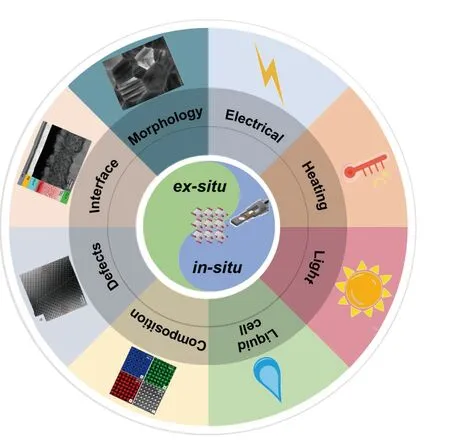
Fig. 1. (Color online) Schematic illustration of advanced TEM characterization for halide perovskites.
2.Irradiation damage on halide perovskites by conventional TEM imaging
The irradiation damage induced by energetic electrons during the imaging of halide perovskites has significantly limited the TEM characterization, and is considered as the cornerstone for the interpretation of as-observed microstructures.
When organic–inorganic hybrid perovskites are imaged using conventional TEM, the structure of the halide perovskites can be destroyed in seconds, resulting in the irradiation damage such as generation of "bubbles" and precipitation of nanoparticles, as shown in Fig. 2. Chenet al. noticed severe damage in the MAPbI3perovskite polycrystalline film when imaged at a relatively high electron dose of ~9870 e/(Å2·s) (i.e.the dose for obtaining conventional HRTEM images), where nanoparticles precipitated quickly within the irradiated area(Fig. 2(a)). Such irradiation damage was attributed to the electric field generated by the electron beam within the perovskite, and remained by reducing electron dose to 500 e/(Å2·s)[47,48]. On the other hand, Kimet al. revealed the generation and expansion of "bubbles" by obtaining a series of TEM images through continuous irradiation on MAPbI3perovskite single crystals (Fig. 2(b))[49]. In general, the degradation of organic–inorganic hybrid halide perovskites in vacuum or in air has been frequently noticed, and the precipitated nanofragmentaions are mostly identified mostly as PbI2or Pb clustering[50,51]. In addition, 2D organic-inorganic hybrid halide perovskites are more susceptible to electron beam damage due to the presence of interlayer organic ligands, and very few TEM studies on 2D perovskites were reported. Douet al. attempted to study (C4H9NH3)2PbBr4(i.e. BA2PbBr4) by TEM,which degraded rapidly into Pb nanoparticles under a very low dose[52]. Nieet al. reported the same phenomenon in the study of BA2PbBr4nanosheets, where the nanoparticles quickly precipitated and the nanosheets were amorphized even at low magnification, as shown by time series TEM in Fig. 2(c)[53].
Irradiation damage is also frequently noticed in all-inorganic halide perovskites. Taking CsPbX3for example, Liet al.found that even short time of exposure could cause "dark spots" to emerge at the corners of the quantum dots (QDs)when imaging CsPbCl3, CsPbBr3and CsPbI3QDs as shown in Fig. 2(d)[54]. The emerged "dark spots" were confirmed as PbX2nanoparticles, as reported in other related works as well[55−58]. Further analysis inferred that the irradiation-induced precipitation of PbX2was due to the surface defects on nanoparticles, and could be effectively suppressed by ZnX2/hexane treatment which "repaired" the halogen ion defects[54]. Similarly, Wanget al. reported a layer-by-layer decomposition of CsPbBr3which also started from the surface, confirming the impact of surface passivation[58]. Continuous irradiation may further cause phase separation and lead to amorphization in nanocrystals as revealed by Funket al.[59]. Similarly,Danget al. studied CsPbX32D nanosheets and 1D nanowires by HAADF-STEM imaging, and also reported the precipitation of nanoparticles, at low dose of 400 e/Å2under both 80 and 200 kV[56]. The degradation mechanism of CsPbBr3under electron beam irradiation was proposed to be dominated by decomposition coupled with knock-on damage: the incident electrons first led to the desorption of halogen ions and reduced Pb2+to Pb0partially; Pb0then migrated and aggregated to form precipitation of Pb; finally, the CsPbBr3collapsed and became amorphized, as illustrated in Fig. 2(e).

Fig. 2. (Color online) (a) Electron beam irradiation damage observed in free-standing MAPbI3 films. (i, ii). TEM images recorded initially and after the irradiation (9870 e/(Å2·s) for ~2 min), respectively[47]. (b) Time-series of TEM images on MAPbI3 single crystal showing the electron beam damage from 0 to 50 s, where bubble-like morphology (colored arrows) emerged and grew[49]. (c) Time-series of TEM images obtained on BA2PbBr4 nanosheets[53]. (d) TEM images of the (i) CsPbCl3, (ii) CsPbBr3 and (iii) CsPbI3 QDs where "dark spots" present at the QD corners indicated irradiation damage[54]. (e) Schematic illustration of CsPbBr3 degradation pathway[56].
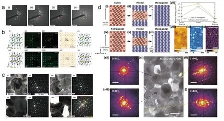
Fig. 3. (Color online) (a) Degradation of MAPbI3 studied using SAED taken from a near-<10> t-oriented grain: i) the initial, pristine phase and ii)after 1 min (total dose per area of ≈1 × 10² e/Å2), iii) 2 min (total dose per area of ≈2 × 10² e/Å2), iv) 18 min (total dose per area of ≈2 × 10³ e/Å2)of weak electron beam exposure (≈2 e/Å2)[46]. (b) Degradation in MAPbX3 by forming superstructured intermediate phase: i) atomistic structure of tetragonal MAPbI3; ii) electron diffraction (ED) pattern along the [001]c direction; iii) the observed ED of superstructure phase; iv) the simulated ED of superstructure phase MAPbI2.5; v) the corresponding atomistic structure; vi) atomistic structure of MAPbBr3; vii) ED pattern along the[001] direction; viii) the observed ED pattern with additional reflections; ix) the simulated ED of superstructure phase MAPbBr2.5; x) the corresponding atomistic structure with ordered bromine vacancies[69]. (c) TEM images and [110] oriented-SAED patterns taken from grain highlighted in yellow circles from FAPbI3 films with (i, ii) 10% MA, (iii, iv) 20% MA, (v, vi) 30% MA, (vii, viii) 40% MA[78]. (d) Stabilization of photoactive perovskites against degradation by tilted octahedral, as illustrated by structural model (i–vi), calculated energy difference (vii), AFM-IR characterization(viii–x), and TEM imaging (xi) with corresponding SAED (xii–l)[79].
More recently, Pb-free halide perovskites with a double perovskite structure are being developed, such as Cs2AgBiBr6,Cs2CuSbCl6, Cs2AgInCl6. Zhouet al. synthesized Cs2CuSbCl6nanoparticles, and Cruetzet al. synthesized Cs2AgBiCl6, Cs2Ag-BiBr6and CsAgBiI6nanoparticles, and they were all characterized by TEM[60,61]. However, irradiation damage was not alleviated in these structures, if not worse. Quick precipitation of nanoparticles and decomposition was also noticed in these materials even at extremely low dose. It was proposed that the degradation was initially induced by the Knotek-Fabel effect at the surface, and was then followed by decomposition into Cs3Bi2Br9, BiBr3, CsAgBr2and AgBr. When the electron beam dose rate was less than 2 e/(Å2·s), the structure could be maintained for about 4 min as confirmed from electron diffraction. Alternatively, Cs2AgBiBr6lattice image could be obtained under a single exposure with a dose rate of less than 281 e/(Å2·s) using conventional HRTEM[62].
It is generally accepted that the electron dose and dose rate have the most influence on the degradation of halide perovskites under electron irradiation, yet it is interesting to discuss the impact of accelerating voltage, i.e. beam energy. In the damage caused by electron beam radiation, it is generally believed that there are three types of radiation damage mechanisms, that is, knock-on damage, radiolysis, and rise of local temperature caused by phonons excited by electron beam radiation[63,64]. As the latter two factors are more related to electron dose, the first factor is closely related beam energy. Recently, Caiet al. calculated the knock-on damage on hybrid halide perovskites using first principle, and showed that iodine is only knocked-out when accelerating voltage is higher than ~250 kV[65]. This is in contrast to experimental results, where low kV has been performed to study the hybrid perovskites where degradation is not noticeably reduced[56,66,67]. Therefore, it is a strong evidence that radiolysis dominates the degradation of halide perovskites under electron beam irradiation, and low-dose is vital for TEM characterization.
3.Degradation mechanism and defects identification of halide perovskite using electron diffraction
Due to the beam-sensitivity of halide perovskites, selected area electron diffraction (SAED) with the advantage of low dose, has become a powerful tool to study the degradation mechanism and intrinsic microstructures of halide perovskites.

Similar to Rothmann’s work, Chenet al. also studied the degradation process of MAPbI3through SAED time series[68].Whilst degradation from MAPbI3to PbI2was also observed and confirmed, the generation of superstructure diffraction patterns was interpreted due to the formation of ordered halide vacancies, thereby resulting in MAPbI2.5intermediate phase. Moreover, the effects of electron dose and dose rate under the accelerating voltage of 300 kV were compared: at a dose rate of 0.5 e/(Å2·s), MAPbI2.5mesophase appeared in 303 s, and at a dose rate of 1 e/(Å2·s), MAPbI2.5mesophase appeared in 73 s, indicating that the degradation of MAPbI3under electron beam irradiation was not only related to the total dose, but also to the dose rate, and thus a higher dose rate might accelerate the degradation of MAPbI3. The same group of authors continued to study the degradation process of MAPbBr3by SAED and reported a similar degradation process, proposing a general degradation mechanism for MAPbX3as halogen ion desorption → formation of ordered vacancies → formation of MAPbX3–xmesophase → precipitation of PbX2”, as shown in Fig. 3(b)[69]. Similar degradation pathways had been generally recognized in oxide perovskites, but it was first proposed in halide perovskites[70,71]. More recently,similar degradation mechanism was reported in all-inorganic perovskite of γ-CsPbIBr2as well, where an intermediate phase[e.g., CsPb(1−x)(IBr)(3−y)] with a superstructure of ordered vacancies was formed, followed by reduction from Pb2+to Pb0and thus precipitation of Pb nanoparticles[72].
SAED is also used to study the degradation mechanism of 2D nanosheets due to their extreme beam-sensitivity.Yuan et al. studied the structural changes of BA2FAPb2I7and BA2MAPb2I7under electron beam irradiation by recording SAED time series, and proposed the degradation mechanism as following: organic ligands between the nanosheets were firstly destroyed by the electron beam; the organic moieties and [PbBr6] octahedra were then damaged, resulting in the rapid collapse of the structure[73]. The proposed degradation mechanism was confirmed by Nie et al.: by investigating the morphology changes and SAED patterns of BA2PbBr4nanosheets exposed to ultraviolet and white light, the authors found that the organic ligands between nanosheets were most sensitive to light irradiation; further exposure resulted in the tilt of [PbBr6] octahedra and then amorphization.
In addition to the study of degradation mechanism,SAED has been employed to characterize the microstructures of halide perovskites in a damage-free manner. Rothmann et al. discovered the existence of nano-twinning in MAPbI3single crystal by SAED[38]. Li et al. studied the intergrain planar defects in MA1–xFAxPbI3perovskites by low dose electron diffraction, and found that the as-fabricated solar cell performance correlated empirically with the density and structure of {111}cplanar defects and {112}ttwin boundaries[74]. Gao et al. obtained SAED diffraction patterns of BA2PbI4nanosheets with different structures, and obtained the lattice image of 2D nanosheets through filtering and inverse fast Fourier transform[75]. For all-inorganic perovskites, Pan et al. revealed the B-site cations disorder in Cs2AgBiBr6using electron diffraction[76]. Luo et al. combined SAED and nano-diffraction to reveal a partial ordering of Ag/Na cations in Cs2Ag(Na)InCl6single crystal[77]. Using a nano-beam with a diameter of ~5 nm (equal to current density of ~1.6 pA/cm2)and a dwell time of 0.1 s, the authors demonstrated damagefree scanning over the sample for several minutes. Pham et al. unraveled the influence of CsCl/MACl on stabilizing cubic α-FAPbI3phase and minimizing twinning/stacking faults through electron diffraction as shown in Fig. 3(c)[78]. More recently, Doherty et al. revealed that α-FAPbI3stabilized by Cs and MA cations alloying had octahedral tilting of ~2°, which imparted the phase stability by frustrating transitions from photoactive to hexagaonal phases. Such minor tilting was neglected by bulk characterization such as XRD, but was resolved by electron diffraction, as shown in Fig. 3(d)[79].
4.Emerging TEM approaches for halide perovskites at atomic resolution
Driven by the urgent need to understand the structureproperties relationship of halide perovskites, novel approaches on both hardware and methodology are being developed to overcome the limits opposed by electron dose,and to further push the spatial resolution down to atomic scale.
With regard to the degradation mechanism of halide perovskites under electron irradiation, it is generally accepted that: (1) the electron dose and dose rate are dominating the irradiation process, and therefore low-dose imaging is essential; (2) the disassociation of organic ligands and halide ions is the first to trigger decomposition of halide perovskites. In light of these understandings, various methods have been proposed to push HRTEM imaging of halide perovskites towards atomic scale, including: (1) deposition or coating of carbon film to alleviate the radiolysis damage; (2) improvement on detectors such as direct electron detector to enable ultra-lowdose imaging; (3) developments of low-dose imaging techniques such as exit-wave reconstruction, ptychography, and iDPC etc.
Above-mentioned techniques have demonstrated to be successful in resolving pristine structures of halide perovskites at atomic scale. Yu et al. revealed the microstructure of CsPbBr3by defocus series at a low dose rate of ~100 e/(Å2·s) under accelerating voltage of 80 kV[41]. As shown in Fig. 4(a), nano-domain with the co-existence of cubic phase and orthogonal phase was demonstrated. Brennan et al. further applied the same approach onto CsPbBr3nanocubes and reported a size dependency on the crystal phases[80]. Alternatively, Zhang et al. employed a direct-detection electron-counting camera to obtain the first atomic resolution image of MAPbBr3at a total dose of only 11 e/Å2, revealing nanodomain structure where the MA+cations were ordered locally in the single crystal, as shown in Fig. 4(b)[39,81]. Chen et al. also used direct-detection electron-counting camera to investigate the decomposition pathway of MAPbI3at atomic scale, where the intermediate phase of MA0.5PbI3with locally ordered vacancies was successfully imaged[82]. Alternatively, iDPC has been demonstrated to be helpful in revealing the atomic structures of halide perovskites: an early iDPC-STEM attempt for the investigation of MAPbBr3was performed by Song et al., enabling low-dose imaging at atomic scale[81];more recently, Qiao et al. demonstrated the magnified iDPCSTEM image could clearly distinguish the atomic distributions of Cs, Pb, and Br from monodispersed CsPbBr3nanocrystals, as encapsulated and stabilized in metal-organic framework[83]. Recently, ptychography has been applied to image halide perovskites due to its advantage of low dose. As shown in Fig. 4(c), the presence of Br was revealed at atomic scale[84]. It is interesting to mention that pulsed-beam TEM has been demonstrated on studying MAPbI3, where the dose could be controlled as low as 0.001 e/Å2[85]. Although the spatial resolution is rather low compared to HRTEM, it offers a possibility for damage-free study of halide perovskites.
Thanks to the development of low-dose imaging technique, defects in halide perovskites have been imaged in detail as never before. Caiet al. recently succeeded in imaging grain boundaries of MAPbI3PSCs at atomic scale by developing a coating approach onto FIB-prepared cross section, as shown in Fig. 4(d)[86]. The carbon coating can significantly inhibit the loss of volatile substances such as CH3NH2and halogens. It was suggested by Chenet al. that depositing carbon film with a thickness of ~6–10 nm on MAPbI3could increase its tolerance against electron irradiation by nearly 10 times[69]. On the other hand, Shiet al. successfully resolved the atomic structure on (2T)2PbI4–(2T)2PbI4–(2T)2PbBr4heterojunction nanosheets, through continuous exposure at extremely low dose and subsequent superposition of time series[87]. In this manner, HRTEM images with a high signal-tonoise ratio were obtained under a total dose of only 9.2 e/Å2,and defects at the heterojunction interface were revealed at atomic scale as shown in Fig. 4(e). Recently, Junget al.revealed the growth of polytypic PbI2on the surface of 2D Ruddlesden-Popper halide perovskites BA2MA2Pb3I10, where a sequential layer-by-layer degradation from perovskites to PbI2was imaged at atomic scale[88]. CsPbBr3nanocrystals were also studied by HAADF-STEM, where Ruddlesden-Popper stacking fault was revealed by a beam current of 50 pA at an accelerating voltage of 300 kV[89,90]. The author mentioned that a short dwell time of 3–6μs can suppress irradiation damage. Additionally, Rothmannet al. used low-angle annular dark field STEM (LAADF-STEM) to study FAPbI3thin films, and successfully imaged grain boundaries at atomic scale as shown Fig. 4(f)[67]. It was suggested by the authors that LAADF-STEM could effectively lower the beam damage on halide perovskites, and therefore might find more applications in resolving atomic structure of beam-sensitive materials.
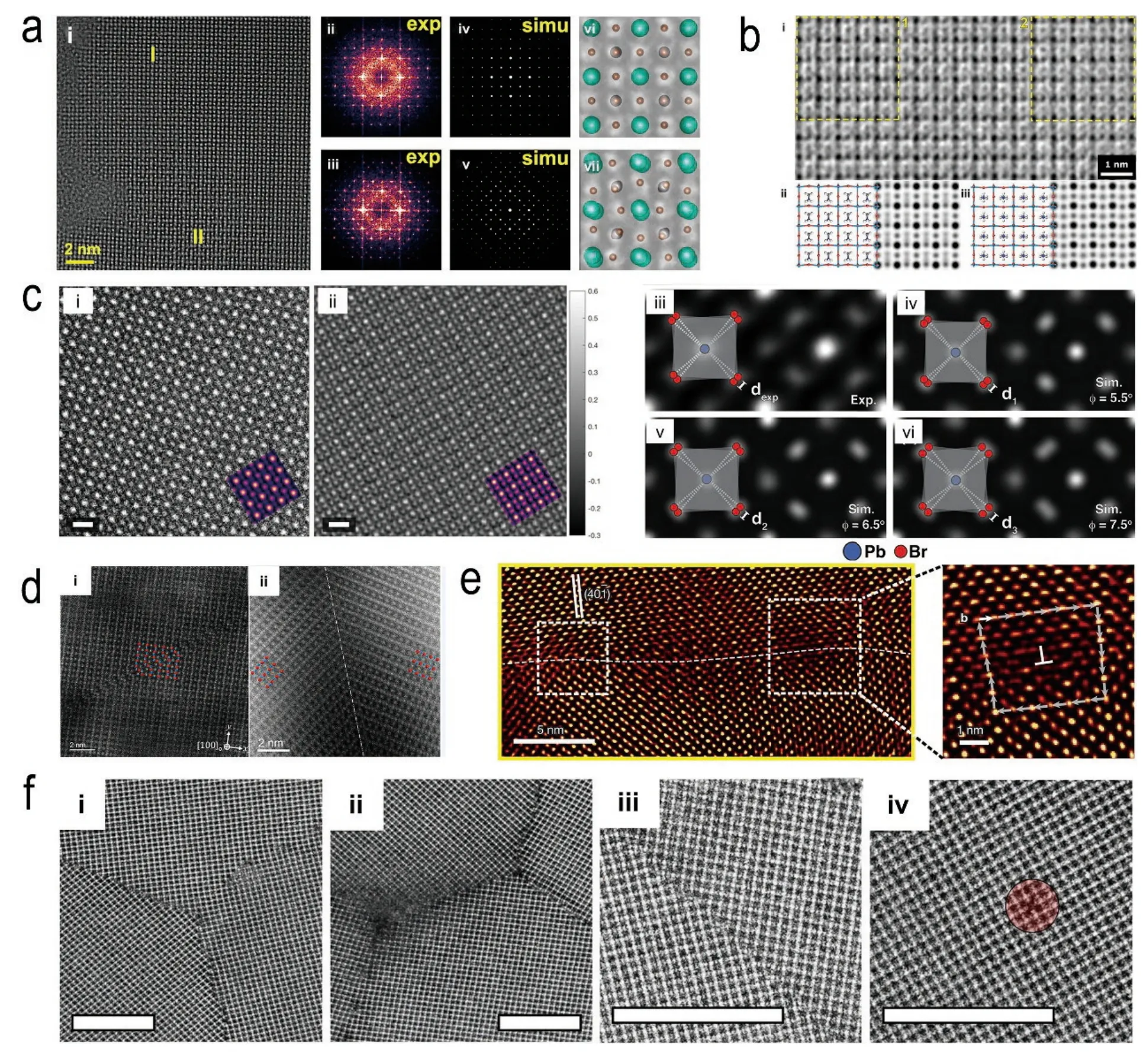
Fig. 4. (Color online) (a) HRTEM of CsPbBr3 nanocrystals (i) where the coexistence of cubic and orthorhombic phases were demonstrated by FFT patterns (ii, iii), simulated diffraction patterns (iv, v), and illustrated structure (vi, vii)[41]. (b) CTF-corrected denoised HRTEM image (i) of CH3NH3Pb-Br3 with different CH3NH3 orientations, where (ii, iii) the structural model (left) and the simulated projected potential map (right) corresponding to region 1 and 2 in (i), respectively[39]. (c) Ptychography reconstructed image of CsPbBr3, with the scale bar of 5Å[84]. (d) Atomic-scale structures of intragrain stacking-fault (i) and twinning interfaces (ii) obtained on orthorhombic FA0.5Cs0.5PbI3 grains along the [100] projection direction[86].(e) Atomically resolved interface at the (2T)2 PbI4–(2T)2 PbI4–(2T)2 PbBr4 heterostructure[87]. (f) Butterworth-filtered LAADF-STEM images of grain boundaries (i), triple junctions (ii), grain boundary (iii) and aligned vacancy defects indicated by red circle (iv), obtained from a 30-nm-thick film of FAPbI3[67].

Fig. 5. (Color online) (a, b) Atomically resolved HAADF-STEM images and corresponding EDX-mappings of CsPbBr3 nanoplates[92]. (c) STEM-EELS from a CsPbBr3 nanosheet to determine bandgap, where (i) demonstrates measured data and (ii) shows as-calculated bandgap value[93].
5.Chemical mapping of halide perovskites using STEM-EDX or STEM-EELS
Due to the beam sensitivity, elemental mapping of halide perovskites has been a standing issue for microstructure investigations. Large dose is often required to obtain enough counts for either EDX-mapping or EELS-mapping, which exceeds the degradation threshold of halide perovskites. Although chemical mapping has been reported in many halideperovskites study, it is also known that the instability of halide perovskites during beam irradiation thus leads to the reliability of elemental mapping, questioning whether the mapped results reflect the pristine structure. Therefore, novel approaches have been proposed to enable the elemental mapping down to atomic scale.
Kosasihet al.performed a systematic study on the evaluation of STEM-EDX quality demonstrated on state-of-art triple-cation, double-halide perovskite with a nominal stoichiometry of Cs0.06FA0.79MA0.15Pb(I0.85Br0.15)3[91]. The acquisition parameters were systematically varied to evaluate the relationship between electro dose, data quality and irradiation damage. It was found that the iodine content decreased exponentially with electron dose, and thus called attention to the interpretation of STEM-EDX mapping results.
In order to minimize electron damage, Liuet al.recently fabricated a highly-beam-stable CsPbBr3nanoplates through an interface-assisted regrowth method using cyanamide[92].By defect-healing self-assembly/regrowth processes and surface passivation by cyanamide molecules, the as-prepared CsPbBr3was demonstrated to be highly stable against electron beam irradiation and thus achieved elemental mapping at atomic resolution, as shown in Figs. 5(a) and 5(b). The stability improvement as shown in this work demonstrates that the beam damage starts from the surface, where surface passivation and defect-healing can effectively suppress the radiolysis damage, although further experiments are needed to check the universality of this method.
On the other hand, STEM-EELS has been demonstrated on orthorhombic CsPbBr3to determine bandgap as shown in Fig. 5(c)[93]. Care was taken in spreading the electron dose for the EELS experiments so to minimize irradiation damage, and the beam current was set to be <5 pA. Meanwhile, the spectra were collected by summing up individual datapoints from spectrum images acquired over a large sample area. By this mean, the spectra with a high S/N ratio could be collected for accurate bandgap determination. Interestingly, bandgap increase was found at nanoplates with thickness below 10 nm,and thus confirming 1D confinement in nanosheets. More studies using EELS or EDX are foreseen to contribute to the studies of halide perovskites.
6.Fast-developing cryogenic TEM for halide perovskites
Cryogenic TEM (cryo-TEM) has been developed rapidly in recent years. Beyond life science, its development has also offered opportunities to materials science, particularly to those too sensitive for conventional HRTEM and related spectroscopy[94]. Growing applications are found for energy-related materials in past few years, and halide perovskites are benefitting from cryo-TEM as well[95].
Liet al. combined the cryogenic temperature with direct electron detector dedicated for low-dose imaging, and successfully obtained HRTEM of MAPbI3and MAPbBr3under the dose of 12 e/Å2and 46 e/Å2[48]. Zhuet al.investigated the MAPbI3single crystal at atomic scale using cryo-TEM, where electron dose rate was kept at ~47 e/(Å2·s) for about 2 s[96]. Defects of surface steps and high density of stacking faults were revealed and correlated to the optoelectronic behavior of charge separation and carrier recombination (Fig. 6(a)). The same group further studied the formation of halide perovskites in the initial nucleation stage using low-dose imaging by cryo-TEM, as demonstrated on both MAPbI3and MAPbBr3respectively (Fig. 6(b)). A growth pattern from initially stacked slices towards a perfect single crystal structure was revealed, proposing a so-called twist-to-untwist structural evolution[40,97]. Low-temperature imaging was also applied to all-inorganic perovskites such as CsPbBr3[98]. The degradation mechanism was proposed as following: the migration and aggregation of Pb were suppressed at low temperature, and degradation was then dominated by the desorption of halogen ions induced by incident electrons, which led to decomposition products of CsBr, CsPb and PbBr2nanoparticles;further irradiation caused the formation and growth of pores and thus destroyed the structure. Additionally, it is interesting to mention that cryo-FIB has been applied to prepare specimen for atom probe tomography[99]. More recently Zhouet al. reported cryo-FIB preparation of a MAPbI3single crystal film solar cell cross-section, enabling high quality microstructural investigation by electron diffraction[100]. Damage-minimized sample preparation by cryo-FIB is thus expected to find more applications in the cross-section preparation of PSCs for more reliable microstructural investigation.
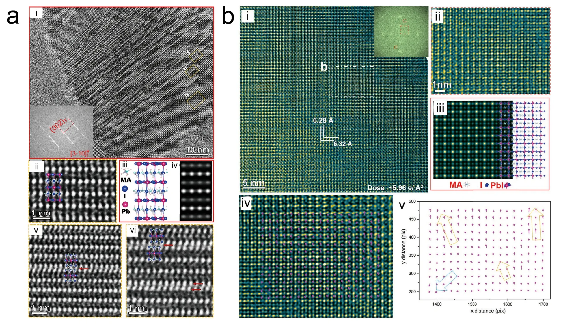
Fig. 6. (Color online) (a) Stacking faults observed in a MAPbI3 with corresponding FFT patterns as inset (i), and corresponding magnified HRTEM(ii, v, vi) with structural model (iii) and (iv) the simulated HRTEM image[96]. (b) Atomically resolved-cryo-TEM image of aged MAPbI3 collected at a low dose condition (electron dose, ~5.96 e/Å2), with corresponding enlargement (ii, iv), structural model (iii) and polarization map (v)[40].
Nevertheless, it should be noted that the use of cryogenic temperature for halide perovskites imaging remains an open issue. It was reported by Rothmannet al. that low temperature could not alleviate irradiation damage but led to rapid amorphization of MAPbI3[46]. Similar results were reported on FAPbI3thin films, where both room-temperature and cryogenic conditions were performed for imaging, but beam sensitivity was not noticeably reduced in the cryogenic conditions[67]. Therefore, detailed studies on the imaging conditions and degradation pathways in the cryogenic conditions are still needed towards further developments.
7.In-situ TEM dedicated to reveal degradation of halide perovskites under environmental conditions
Although much progress has been achieved in resolving the microstrure of as-grown halide perovskites or as-fabricated photovoltaic devices from nanoscale down to atomic scale, there is an urgent need to study the structural evolution of halide perovskites based devices under external stimuli such as light, heat and moisture so to understand the degradation of perovskites under environmental factors[101−104].In-situTEM is thus considered as a powerful tool to this end, and has achieved significant progress in the past few years[3,105,106].
The thermal stability of halide perovskites can be studied byin-situheating in TEM. As demonstrated by Divitiniet al., the morphology and chemical composition change of MAPbI3-based PSC during elavating temperature (up to 250 °C) was monitored using a FIB prepared cross-section(Fig. 7(a))[42]. Migration of I and Pb was revealed and correlated to the synthesis condition. Seoet al. further compared the thermal responses of Csx(FAyMA(1–y))(1–x)Pb(IzBr(1–z))3to MAPbI3PSCs usingin-situheating, and found that MAPbI3degraded rapidly by forming particles and voids, whereas FAbased PSCs is more heat-resistant. Similarly, the thermal stability of inorganic perovskites has been demonstrated on CsPb-Br3, and found a superb stability up to 690 K[107].
The impact of curent–voltage stimulus on perovskites degradation can be investigated byin-situbiasing. MAPbI3-based PSC was prepared into cross section and subjected to biasing in TEM by Jengroset al.[108]. Degradation was identified particularly at the positively biased MAPbI3interface,where iodide migrated into the transport layer and volatilized, resulting in the nucleation of PbI2nanoparticles and voids. MAPbI3interface with TiO2as electron transport layer was further studied usingin-situbiasing combined with HRTEM and STEM-EELS (Fig. 7(b))[109]. It was found that positive bias led to oxygen diffusion into the MAPbI3layer accompanied with performance degradation, wheras a negative bias could remove oxygen ions from MAPbI3and partially restored the performance. Kimet al. observed amorphization of perovskite layer byin-situbiasing as induced by ion migration, whereas the bias-introduced degradation could be healed by heating at 50 °C[110]. More recently, anin-situelectrical probing and light illumination through an optical fiber was applied to study the optoelectronic and photovoltaic properties on different crystal facets of CsPbBr3[111]. This work demonstrated a possibility of studying light-introduced degradation of perovskites.
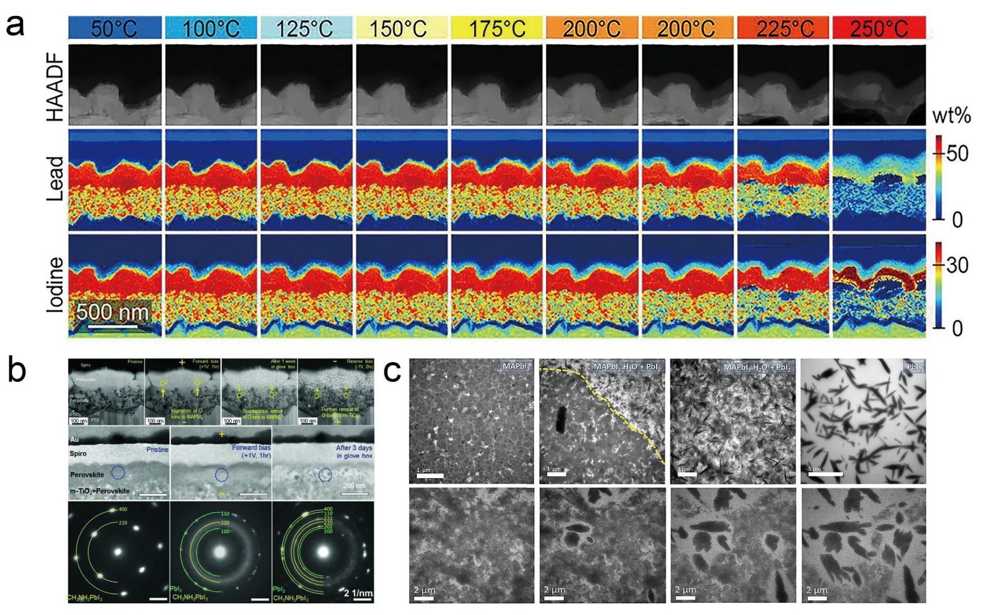
Fig. 7. (Color online) (a) In-situ heating of MAPbI3 based PSCs up to 250 °C, where the temperature evolution of morphology change and elemental migration was monitored by HAADF-STEM images and EDX mappings. The same scale bar applies to all panels[42]. (b) In-situ electrical biasing on MAPbI3, where morphology and structure change was monitored by HAADF-STEM, TEM and SAED, respectively[109]. (c) In-situ TEM showing the impact of controlled humidity on the conversion of MAPbI3 into MAPbI3·H2O and finally PbI2, using liquid cell[112].
Last but not least, the moisture-induced degradation was recently studied using in-operando liquid cell TEM (Fig.7(c))[112]. A live visualization from meso-to-nanoscale transfomration between prototypical MAPbI3and water molecules was presented: intermediate phase of MAPbI3·H2O was first formed upon exposure to humidity, and was subsequently decomposed into PbI2crystals through dissolution/recrystallization. In addition,in-situliquid cell TEM has been used to study the nucleation of pervoskites as demonstrated on MAPbI3as well, providing useful reference for understanding the intriguing chemical and physical properties of halide perovskites[113].
8.Conclusions and perspective
This review summarizes the recent progress of advanced TEM characterization for halide perovskites. The main conclusions are as following.
(1) Due to the presence of halogen ions and organic moieties, halide pervoskites are extremely sensitive to electron beam irradiation. Conventional TEM causes degradation in almost all halide perovskite structures, showing "artifacts" and damage such as the generation and expansion of holes, grain boundary cracking, and nanoparticle precipitation. Although the degradation mechanism under electron beam interaction remains unclear, it generally follows the pathway of "electron beam incidence → organic moieties and/or halogen ion desorption → defect generation and expansion → lattice collapse and amorphization → PbI2or Pb precipitation". Both electron dose and dose rate have impact on the degradation. The understanding of degradation is essential, as it calls attention to the interpretation of TEM results and ultra-care in performing TEM characterization.
(2) In order to reduce the irradiation damage, low-dose is vital for halide perovskites’ characterization. Electron diffraction has shown to be powerful in resolving the crystal structure and microstructure at low dose. In Table 1–4, we have summarized the imaging conditions as reported in this review according to perovskite chemistry, i.e. MAPbI3, MAPbBr3,all-inorganic CsPbBr3/CsPbI3, and 2D halide perovskites, as an imaging guide for researchers in this field. More importantly,safe dose and damage dose for different perovskite materials are summarized in Fig. 8, where dose limit for imaging is better represented. 2D perovskites are most sensitive to electron dose, whereas MAPbI3and MAPbBr3is slightly more robust, and CsPbBr3has the best tolerance to beam irradiation.It is important to note that dose rate and accelerating voltage also has influence on imaging, and surface treatment to protect the sample can drastically increase the critical dose. Readers are encouraged to refer to the tables and corresponding references for specific notes. Undoubtedly, halide perovskites is one of the most beam-sensitive materials,and researchers are encouraged to carefully design and prepare their TEM experiments in order to achieve meaningful results.
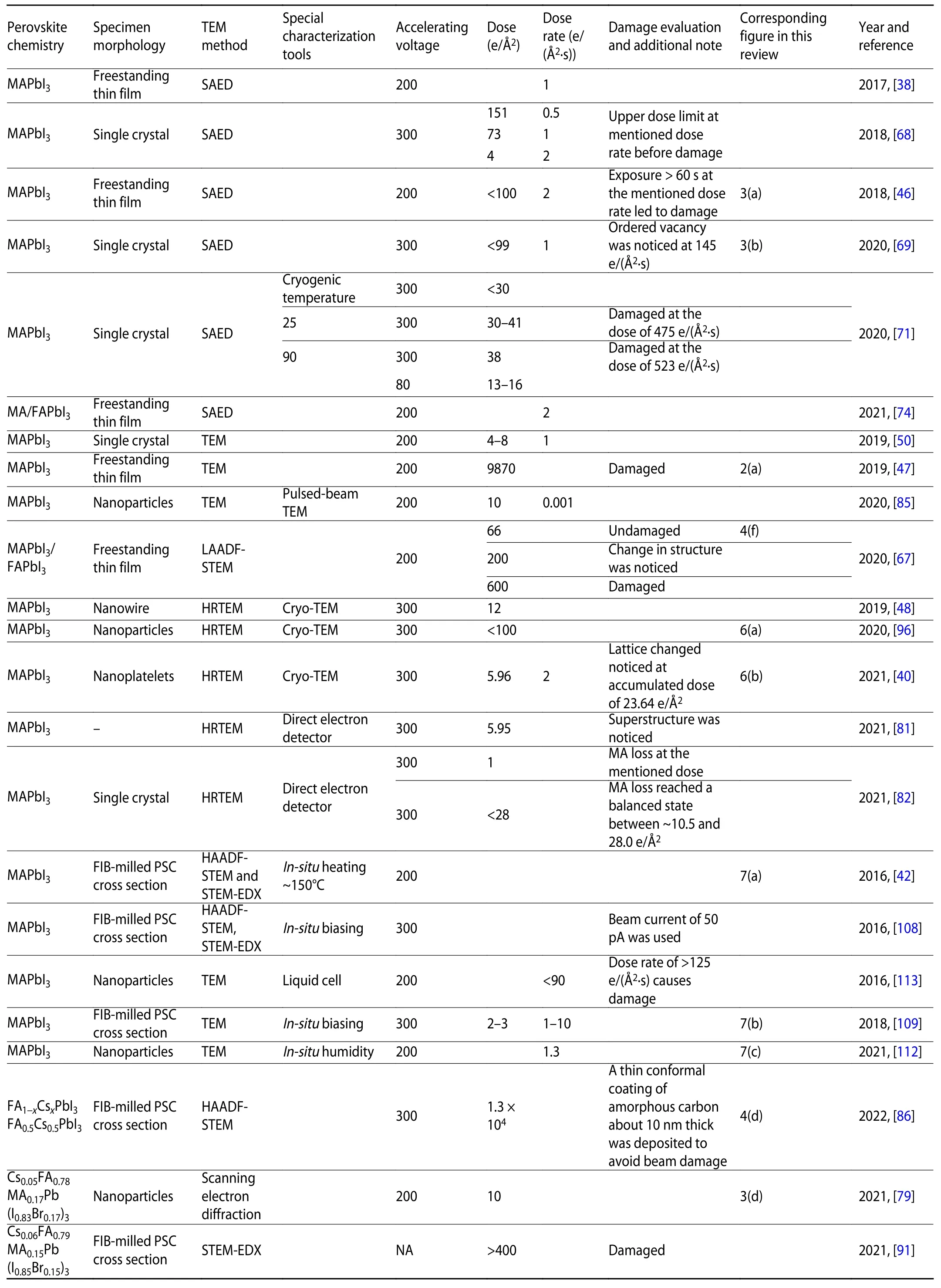
Table 1. Summary of TEM characterization details for MAPbI3 and related structures. No damage or little damage was reported unless specified in the table.
Table 2. Summary of TEM characterization details for MAPbBr3. No damage or little damage was reported unless specified in the table.
Table 3. Summary of TEM characterization details for all-inorganic CsPbBr3 and related structures. No damage or little damage was reported unless specified in the table.
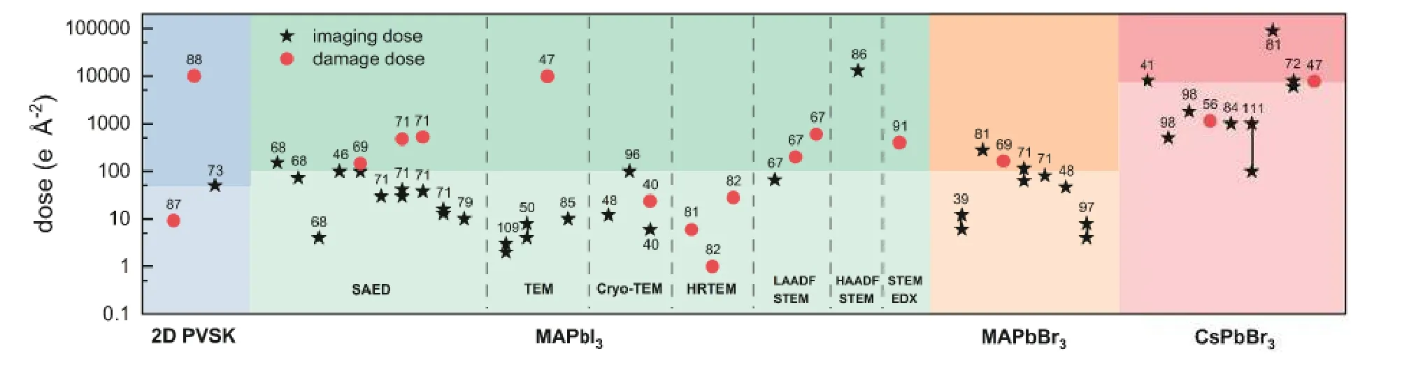
Fig. 8. (Color online) Illustrated summary of safe dose and damage dose for different perovskite materials, plotted in coloured columns. Numbers in the figure correspond to the reference numbers as listed in the tables and references. Shade in each column indicates relatively-safe dose range versus damage-prone dose range. Generally speaking, 2D pvsk is suggested to be imaged below the dose of 50 e/(Å2·s), MAPbI3/ MAPbBr3 below ~100 e/(Å2·s), whereas CsPbBr3 can tolerate dose up to more than 1000 e/(Å2·s).
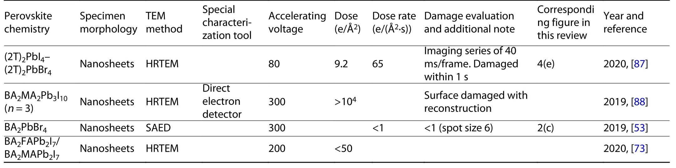
Table 4. Summary of TEM characterization details for 2D halide perovskites. No damage or little damage was reported unless specified in the table.
(3) Emerging techniques have been developed to enable atomic-resolution imaging and chemical mapping of halide pervoskites. Low-dose imaging techniques such as exitwave reconstruction, LAADF-STEM and ptychography has successfully imaged perovskites at atomic scale. The development of hardware such as direct electron detectors have also succeeded in providing atomically resolved structure of halide perovskites. Additionally, the rapid development of cryo-TEM has emerged as a powerful tool to study the halide perovskites and reveal defects such as grain boundaries and surface steps.
(4)In-situTEM under heating, biasing and liquid cell is being developed and applied to study the degradation of halide perovskites under operando conditions. Microstructural change has been revealed with unprecedented details.
Thanks to the rapid developments of emerging TEM techniques, halide perovskites have been resolved down to atomic scale with unprecedented details. Perspectives of TEM characterizations for halide perovskites are proposed as following:
(1) Sample preparation. Imaging techniques such as iDPC, ptychography, and the developments of detectors have paved ways for low-dose imaging, but the bottleneck is sample preparation, particularly for PSC thin films. Conventionally, FIB is used to prepare cross sections, but beam damage of Ga+ions can induce significant damage to the sample prior to imaging. The use of cryo-FIB and surface passivation has shown their advantages in alleviating beam damage, and more studies are encouraged.
(2) Development of emerging techniques. Although lowdose imaging andin-situTEM has been demonstrated to reveal the structure-property relationship, the studies are still limited to a few examples. More investigations on different materials and devices are expected.
(3) Interpretation of TEM data. Degradation mechanism has been discussed in this review, emphasizing the impact of electron dose/dose rate on halide perovskite structure. It is clear that only low dose imaging can reveal the halide perovskite structure, although conventional TEM imaging and EDX/EELS study involves large dose, which significantly exceeds damage threshold. Therefore, we call attentions to the interpretation of TEM data as reported in literatures, where attentions should be paid to the imaging condition before correlation to the conclusions.
Halide perovskites are strategically important in the field of energy materials. Along with the rapid development of the materials and related devices, there is an urgent need to understand the structure-property relationship from nanoscale to atomic scale. Much effort has been made in the past few years to address the beam-sensitivity of this particular materials, and more applications of emerging TEM characterizations are foreseen in the coming future, unveiling the structural origin of halide perovskite’s unique properties and degradation mechanism under operando conditions, so to assist the design of a more efficient and robust energy material.
Acknowledgements
X.K. and M.S. acknowledge the Beijing Municipal High Level Innovative Team Building Program (IDHT20190503) and the National Natural Science Fund for Innovative Research Groups of China (51621003). X.W. and X.K. acknowledge the National Natural Science Foundation of China (12074017).
杂志排行
Journal of Semiconductors的其它文章
- Stabilizing α-phase FAPbI3 solar cells
- Preface to the Special Topic on In-Situ and in-operando Characterization of Semiconductor Materials and Devices
- Janus VXY monolayers with tunable large Berry curvature
- DASP: Defect and Dopant ab-initio Simulation Package
- Structural evolution of low-dimensional metal oxide semiconductors under external stress
- In-situ monitoring of dynamic behavior of catalyst materials and reaction intermediates in semiconductor catalytic processes