Transmission-type reconfigurable metasurface for linear-to-circular and linear-to-linear polarization conversions
2022-12-28PingWang王平YuWang王豫ZhongmingYan严仲明andHongchengZhou周洪澄
Ping Wang(王平), Yu Wang(王豫), Zhongming Yan(严仲明), and Hongcheng Zhou(周洪澄)
School of Electrical Engineering,Southwest Jiaotong University,Chengdu 611756,China
Keywords: polarization conversion,reconfigurable metasurface,Fabry–P´erot resonance
1. Introduction
Polarization is one of the fundamental properties of electromagnetic (EM) waves, which carries plenty of information about the scatters. Thus, the polarization modulation is significant and valuable in many aspects, such as wireless communication,[1–3]radar cross section reduction,[4,5]and imaging.[6,7]To process polarization information as much as possible,the devices which can manipulate multiple polarization are essential. Metasurfaces have provided excellent alternatives. As a two-dimensional artificial material, metasurfaces have been widely utilized to control EM waves because of their low profile,low loss,easy processing,high flexibility,and so on. For possessing tunable property and functionality,various reconfigurable metasurfaces were fabricated by integrating with RF devices[8–16]or functional materials.[17,18]
It has always been pursued to manipulate the polarization of waves at will. To date, various reconfigurable polarization conversion metasurfaces(PCMs)with multiple functions have been proposed. However,the major of reported transmissiontype PCM can only achieve co-polarization transmission and a single polarization conversion. For example, the reconfigurable PCMs composed of periodic rings[8]or chiral structures[9]incorporated with PIN diodes were proposed,which can realize co-polarization transmission and linear-tocircular (LTC) polarization conversion. Some reconfigurable PCMs formed by split rings achieved co-polarization transmission and linear-to-linear (LTL) polarization conversion.[10,11]However, the dynamic switching among LTC and LTL polarization conversions is still rare for the transmission-type PCM. In Ref. [16], the bi-layer PCM incorporated with varactor diodes was proposed, it could convert the incident LP waves into multiple polarization, but it could only operate in narrow frequency band. The integration of LTC and LTL polarization conversions has been concerned.[19–21]To solve the problem, several designs based on passive metasurfaces were reported.Unfortunately,their operational bands for each function cannot overlap,which causes the reported designs impossible to process multi-polarization signals with the same frequency. The design proposed in Refs.[22,23]can reconfigure the incident linear polarization to multiple linear and circular polarization by rotating the metasurfaces,but the slow mechanical adjustment may be limited in applications.
In this paper,we design a novel transmission-type reconfigurable PCM based on Fabry–P´erot(F–P)resonate cavity for LTC and LTL polarization conversions. The proposed PCM consists of a layer of grating, a polarization conversion surface and a reconfigurable polarization selective surface. The switching of functions is realized by changing states of the PIN diodes. To verify the design,the prototype has been fabricated and tested. As demonstrated by the measurement results,the PCM can convert linear polarized(LP)waves to CP waves from 3.31 GHz to 3.56 GHz with the axial ratio (AR)less than 3 dB when the PIN diodes are switched off. Instead,when the diodes are switched on, the PCM can rotate the LP waves to cross-polarized waves from 2.76 GHz to 4.24 GHz with the polarization conversion ratio(PCR)higher than 0.95.The operational bandwidths are 7.3%and 42.3%for the LTC and LTL polarization conversions. The thickness of proposed PCM is 0.2λ0(λ0is the wavelength corresponding to the central frequency). Moreover, the F–P resonance excited in the PCM is discussed in this paper, and the conditions for realizing LTC polarization conversion are also derived. Before our work,a lot of LTL polarization converters combining F–P resonate cavity have been proposed.[24–26]Nevertheless, to the best of our knowledge, the transmission-type LTC polarization converter based on F–P cavity-like metasurface has not been reported. Our proposed design provides a new method for converting incident linear polarized wave into circular polarized and cross-polarized wave,which may promote the development of transmission-type metasurface toward arbitrary polarization manipulations.
2. Analysis and design
2.1. Operational principles of the PCM
For achieving dynamically switching among LTC and LTL polarization conversions, we propose an approach for constructing the PCM whose schematic diagram is depicted in Fig. 1. Layer A is a polarization selector which only permits they-polarized wave to pass through. Layer B is a polarization conversion surface composed of periodic anisotropic structures, which can partially converts the incidenty-polarized wave intoxpolarization. The reconfigurable layer C which integrates PIN diodes has two functions, including co-polarization transmission and polarization selection. The three layers form an F–P resonate cavity. The corresponding relationships between the states of PIN diodes and the PCM are illustrated in Table 1.
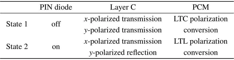
Table 1. Working states of PIN diodes and functions of PCM.
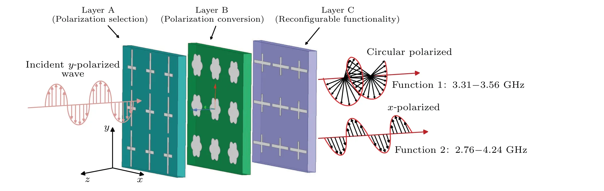
Fig.1. Schematic diagram of proposed PCM for polarization conversion.
Fig.2. The schematic diagram of the propagation of waves in PCM,as the state of PIN diode is switched(a)off and(b)on.
For describing the operational principle, we have established an F–P resonate model based on the PCM as shown in Fig. 2. They-polarized waves illuminate PCM along−zaxis,and the transmission directions of waves in PCM are indicated by the arrows. They-andx-polarized components are denoted by solid and dashed lines,respectively. First,the incidenty-polarized waves pass through layer A and interact with layer B, then the reflected and transmitted waves which includey- andx-polarized components are excited by layer B.They-polarized backward wave penetrates into layer A,thexpolarized one is reflected by layer A and interacts with layer B once again. In contrast, the propagation processes of forward waves depend on states of layer C.If layer C is in state 1, as shown in Fig. 2(a), they- andx-polarized components can pass through it. When layer C is in state 2, as shown in Fig.2(b),only thex-polarized component can pass through it.They-polarized component will be reflected by layer C and undergoes the multiple reflections. It should be noted that the above descriptions of wave propagation in state 1 ignore the reflection of layer C,in fact,a few ofy-andx-polarized components will be reflected by it and participate in the round trips within the PCM.
Based on the analysis of the interactions between waves and metasurface (see Appendix for details), we derived the condition for the PCM achieving LTC polarization conversion as follows:
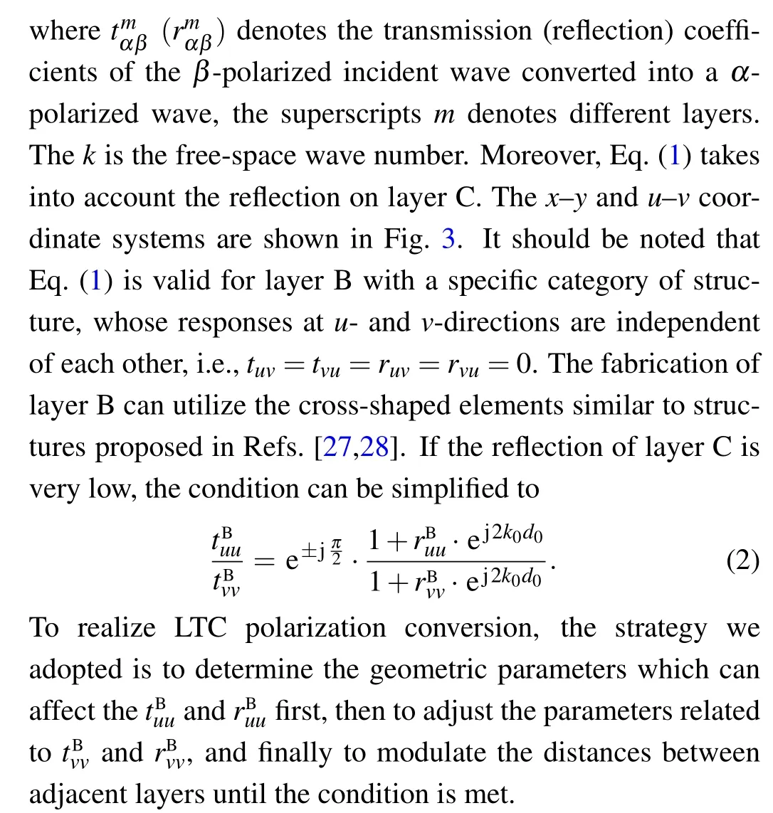
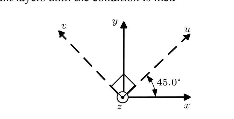
Fig.3. Schematic diagram of the x–y and u–v coordinate systems.
2.2. Design of geometric configuration for each layer
The unit cells of layer A and B are shown in Fig. 4.The dielectric substrates are FR4 with relative permittivityεr=4.3. Several metal stripes alongx-axis are etched on front side of layer A, which form a grating. For filtering out thex-polarized incident waves, the geometry parameters of layer A are chosen asw1=2.5 mm,g1=3.5 mm,the thickness of substrate in layer A ist1=0.5 mm. The metal stripes and successive lines are orthogonal,they are etched on the front side of layer B.The thickness of substrate in layer B ist2=1.6 mm.The equivalent circuits of layer B atu-andv-polarization are illustrated in Fig.5,whereLuandLvdenote the inductance introduced by the metal strips alongu-andv-axis,Cvdenotes the capacitance of the gap between two strips aligned withvaxis.Zsubrepresents the equivalent impedance of the substrate.TheABCDmatrix of layer B can be expressed as[29]
Fig.4. The geometric configuration of unit cell: (a)layer A,(b)layer B.
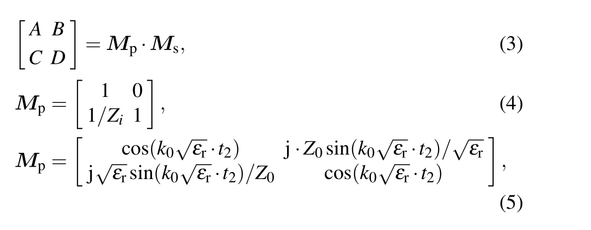
whereMpandMsrepresent the transmission matrix of metal patterns and substrate of layer B.Zidenotes the impedance of metal patterns withi=uori=vdepending on the polarization direction. The impedance can be derived asZu= jωLuandZv= j(2ωLv −2/ωCv). The circuit parameters can be obtained as follows:[14,30]
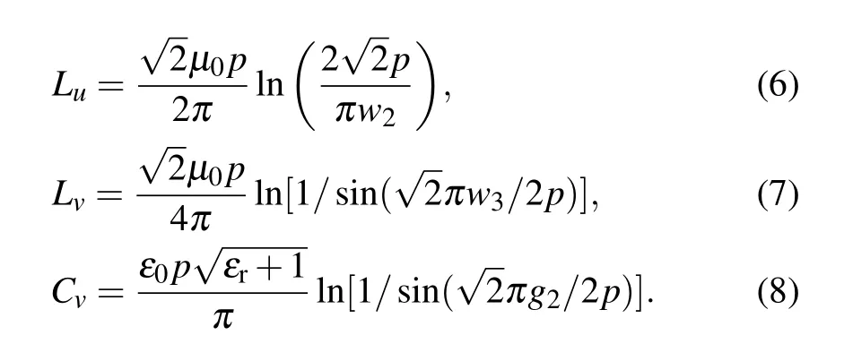
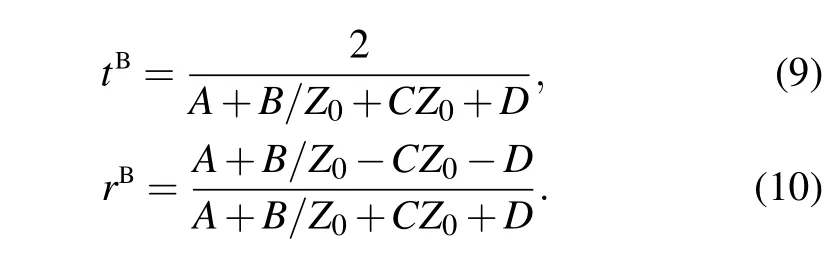
Then,the co-polarized transmission and reflection coefficients of layer B can be calculated by
Via adjusting thew2andg2, the co-polarization transmission and reflection coefficients aligned withu- andv-axis can be independently tuned. The value selections ofw2andg2according to performance of layer B will be described in the following section.
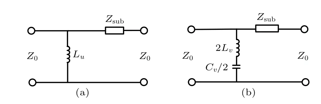
Fig.5. The equivalent circuit model of layer B.The incident wave is(a)u-polarized(b)v-polarized.
The periodic structure of layer C is presented in Figs.6(a)and 6(b), the rectangular metal patches are arranged on the front side. The PIN diodes are embedded into the gaps between adjacent patches. The orthogonal metal lines are etched on the back side of layer C. The PIN diode is Skyworks SMP1345-079LF. For the on state, it can be equivalent to a resistor of 2 Ω in series with an inductor of 0.7 nH. For the off state, it can be equivalent to a capacitor of 0.15 pF in series with an inductor of 0.7 nH. The dielectric substrate employed in layer C is same as in layer B.The geometric parameters of layer C are taken asl2=5.13 mm,g3=2.19 mm,w4=3.14 mm,w5=0.5 mm,w6=0.8 mm,w7=0.4 mm,andp1=16 mm. For describing the operational principle of layer C, the lumped circuit elements introduced by the metal patterns are illustrating in Fig. 6(a). HereL1andL3denote the equivalent inductance of the metal patch atyandxdirections, respectively,C1is the capacitor introduced by the gap between patches alongx-axis. The inductances of metal wires on back side are denoted byL2andL4,respectively. When the PIN diodes are switched off, the front-side structures exhibit capacitive responses alongxandydirections,after cascading with the inductive branches on the backside, layer C will exhibit band-pass response for incident waves. While the PIN diodes are switched on, layer C can be equivalent to a metal grating parallel toy-axis for blocking they-polarized waves.The simulated results of layer C are shown in Fig.6(c). With the changing of PIN states,there is obvious discrepancy for the transmission ofy-polarized wave. For the off state,the|tyy|is consistent with|txx|,which are higher than−1 dB within 2.42–3.80 GHz,for the on state,the|tyy|is less than−20.3 dB below 3.80 GHz.
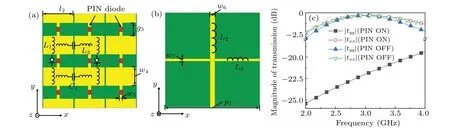
Fig.6. The geometric configuration of periodic structures in layer C:(a)front side, (b)back side. (c)Simulated transmission coefficients of layer C.
2.3. Integrated design of the PCM
By cascading the proposed three layers, as shown in Fig. 7, the PCM is constructed. Then, several geometric parameters need to be determined according to performance of the PCM, including the configuration of the layer B and the distances between adjacent layers. The optimization target for the PCM is to realize LTC and LTL polarization conversions within S-band,and the performances of LTC conversion are set as priority. Based on Eq. (1) and related discussions,the optimizations can follow the principles mentioned below.First, the periodic dimensionpand line widthw2should be determined,which mainly depend on the predetermined transmittance and operational frequency. The increase ofpand the decrease ofw2are conducive to improve the transmittancetBuubecause the equivalent inductances of successive metal lines are raised. However,pshould not exceed half a wavelength in order to suppress the gating lobes.[30]Next, we can optimize the performances of LTC conversion by adjustingg2andd.The frequency responses of the AR with differentg2anddare shown in Fig.8 withp=48 mm andw2=0.1 mm. The AR of PCM is obtained as follows:
It can be found that the minimal value of AR is mainly determined byg2, and the operational frequency is mainly determined byd. We can select the value ofg2first to guarantee the LTC polarization conversion, and then optimize the overlapping bandwidth and conversion coefficients of LTC and LTL polarization conversions by adjustingd. Finally, the performances of PCM can be finely tuned by adjustingd1.The optimized geometric parameters are taken asp=48 mm,w2=1.5 mm,g2=9 mm,d=7 mm,d1=7 mm.
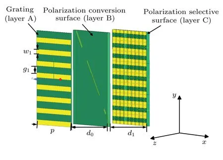
Fig.7. Configuration of unit cell of the proposed PCM.
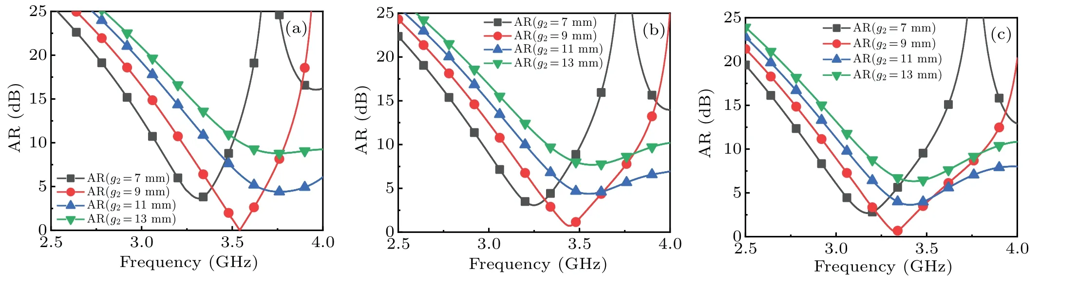
Fig.8. The comparison of AR with different g2 and d: (a)d=5 mm,(b)d=7 mm,(c)d=9 mm.
3. Simulation and measurement results
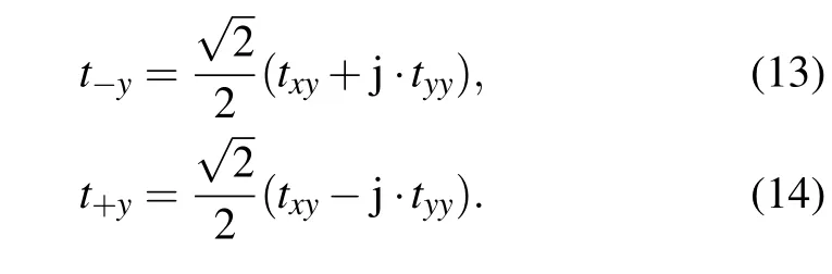
The model of proposed PCM is simulated by the CST Microwave Studio, and the prototype of PCM is fabricated and measured. The experimental setups are illustrated in Fig. 9,two horn antennas are placed on different sides of prototype,which are connected to the Keysight N5227B vector network analyzer (VNA) through RF cables. The size of prototype is 330 mm×330 mm×17.7 mm,and the thickness is 0.2λ0(λ0is wavelength corresponding to the central frequency). The simulation and measurement results are shown in Fig. 10, wheret−yandt+ydenote the transmission fromy-polarized to lifthanded and right-handed circular polarizations, respectively.They can be obtained as follows:
The PCR at LTC and LTL mode is defined as|t−y|2/(|t−y|2+|t+y|2) and|txy|2/(|txy|2+|tyy|2).[10,30]As shown in the measurement results, when the PIN diodes are switched off, the PCM can achieve LTC polarization conversion with the AR less than 3 dB from 3.31 GHz to 3.56 GHz. Meanwhile, the PCR of LTC polarization conversion is higher than 0.95.
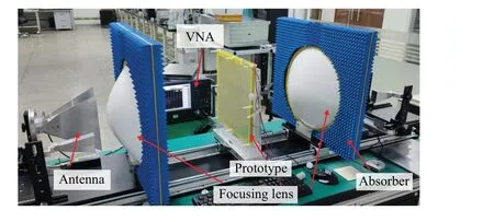
Fig.9. The measurement setup and prototype.
When the PIN diodes are switched on, the PCM can rotatey-polarized wave tox-polarization with the PCR higher than 0.95 within 2.76–4.24 GHz. The fractional bandwidths at LTC and LTL modes are 7.3%and 42.3%,respectively. In the overlapping frequency band, the magnitudes of transmissions of both functions are higher than−1.84 dB.In Fig.10,the measurement results show agreement with the simulation ones, there are some discrepancies which may be caused by the deviations in fabrication of prototype and instrument alignment. Moreover, we obtain the analytic transmission coefficients of PCM according to the discussions in Appendix,which are basically consistent with the simulation and measurement results. Even if there are deviations,the comparison in Fig.10 indicates that the proposed expressions in Appendix can effectively represent the transmission coefficient of PCM.In Appendix,it is assumed that the magnitude of transmittance of layer A toy-polarized wave (the same as the magnitude of reflectivity tox-polarized wave)is 1,whereas the transmittance of layer A in fact will be slightly smaller, which may cause the deviations of the analytic results.
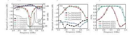
Fig.10. The measurement and simulation results of the PCM:(a)magnitude of transmission and AR for LTC polarization conversion,(b)magnitude of transmission for LTL polarization conversion,(c)PCR for LTC and LTL polarization conversions.
The transmission coefficients of layer B are shown in Fig. 11, where the shadow area indicates the operational frequency band of LTC polarization conversion. It can be found that the magnitude oftBvvrapidly declines with frequency increasing in the operational band. Although the condition of polarization conversion can be satisfied near 3.43 GHz, the sharp change of parameters will limit the functionality to a narrow band. If a metasurface with stable response against frequency is used as layer B, the frequency band will be expanded, such as the multi-resonant structures[31]and multilayer surface,[32]while the profile or insertion loss may be higher than the proposed design. Moreover, if the proposed layer B is replaced by a reconfigurable metasurface with appropriate configuration, the PCM may integrate more functions,such as co-polarized transmission and linear-to-elliptical polarization conversions.
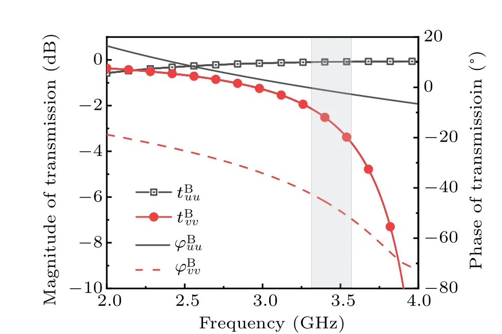
Fig.11. The simulated magnitude and phase of transmission for layer B.
4. Conclusion
In summary, we have proposed a transmission-type reconfigurable PCM as well as detailed procedure,which has the reconfigurable functions of LTC and LTL polarization conversions. The reconfigurable functions are obtained by changing the states of PIN diodes embedded on the PCM. The operation of PCM is based on F–P resonances which have been illustrated. Moreover, to guide the design, the conditions for achieving LTC polarization conversion have been derived.From the measurement results of prototype, the overlapping frequency band of two functions is from 3.31 GHz to 3.56 GHz with the transmission higher than−1.84 dB.The thickness of the proposed PCM is 0.2λ0. Because the transmission-type metasurfaces can be loaded on aperture of the feeding antenna, the proposed design is more suitable for compact system than reflector arrays. It can also quickly switch states due to its electronic adjustment. These advantages make the proposed PCM have the application prospects in S-band radar and satellite communication,meanwhile it also has the potential to merge more functionalities of EM wave manipulation.
Appendix A
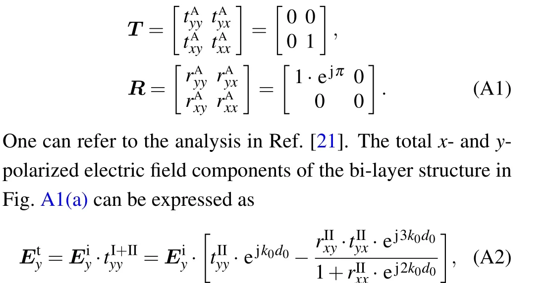
To analyze the propagation of incident waves in the PCM,we divide PCM into two parts at first. As shown in Fig. A1,layer A is named as part I,the layers B and C are regarded as a whole and indicated as part II.Thex-andy-polarized electric field components are denoted byEt/rxnorEt/ryn, wherenin the subscript indicates the component experiencedntimes roundtrips within the space between adjacent layers.We assume that the Jones matrixes describing layer A satisfy
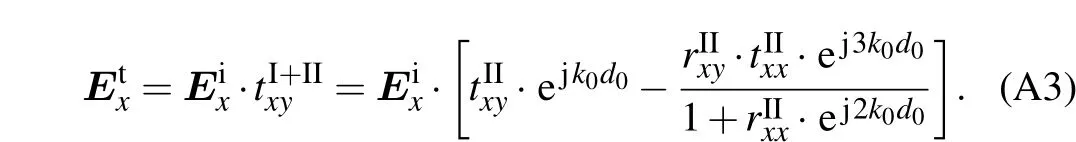
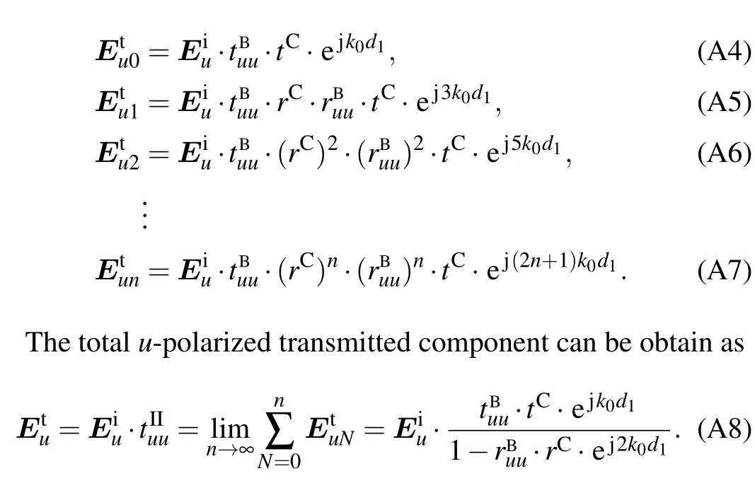
In this paper,the near-field coupling excited between layers is not considered in the analysis of wave transmissions. Next,we present the propagation of waves in part II.The schematic diagram is given in Fig. A1(b). For simplifying analysis, the transmission coefficients in theu–vcoordinate system is discussed first. As mentioned above, the responses of layer B aligned withuandvaxes are independent of each other.Therefore,u-polarized transmitted components can calculated as
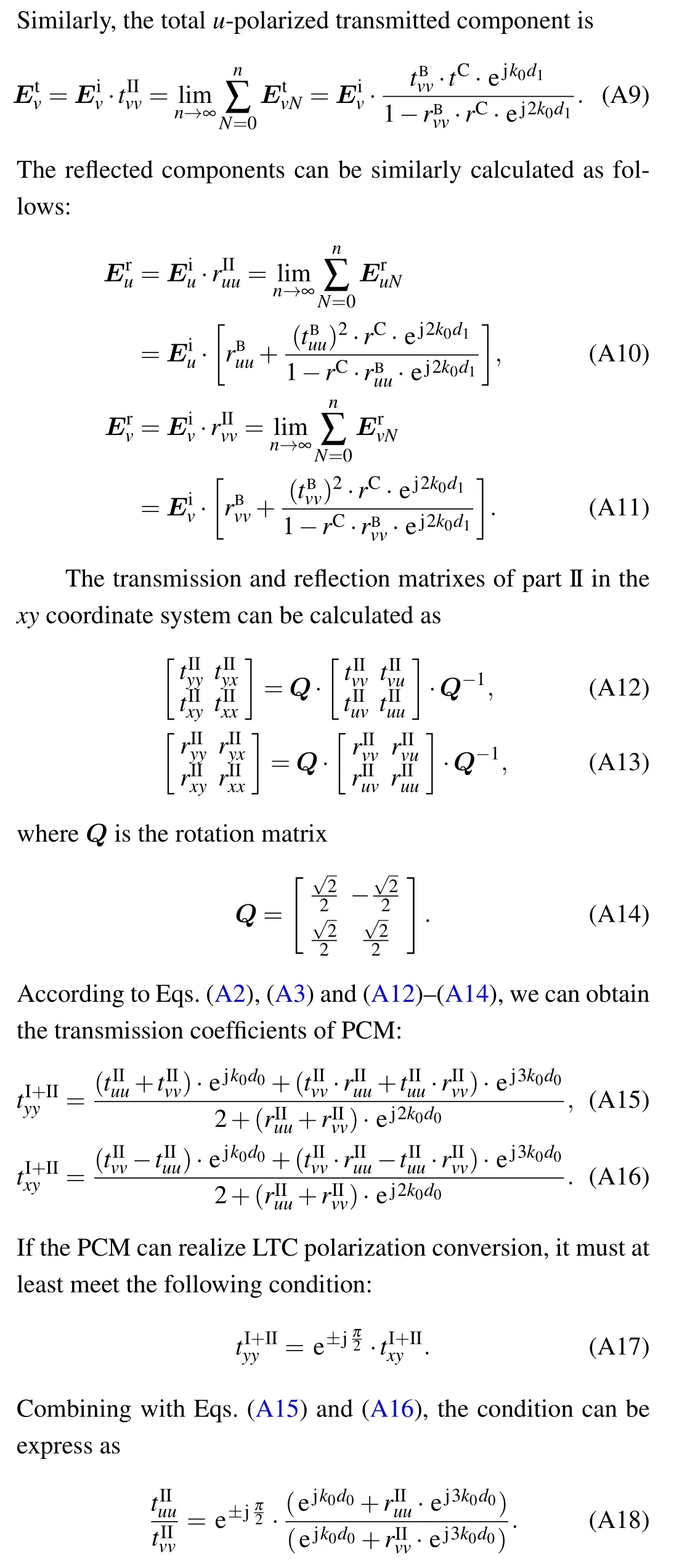
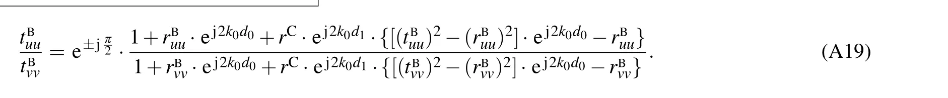
Substituting Eqs.(A8)–(A11)into Eq.(A18),the condition for achieving LTC polarization conversion based on coefficients of each layer can be derived as follows:
Acknowledgement
Project supported by the Fundamental Research Funds for Central Universities(Grant No. 2682020GF03).
猜你喜欢
杂志排行

Chinese Physics B的其它文章
- Editorial:Celebrating the 30 Wonderful Year Journey of Chinese Physics B
- Attosecond spectroscopy for filming the ultrafast movies of atoms,molecules and solids
- Advances of phononics in 20122022
- A sport and a pastime: Model design and computation in quantum many-body systems
- Molecular beam epitaxy growth of quantum devices
- Single-molecular methodologies for the physical biology of protein machines