Hard X-ray focusing resolution and efficiency test with a thickness correction multilayer Laue lens
2022-11-21ShuaiPengYueLiangZhouYiMingYangHongShiBinJiMingLiPengLiuRuYuYanJingTaoZhuGuangCaiChang
Shuai-Peng Yue• Liang Zhou • Yi-Ming Yang • Hong Shi • Bin Ji •Ming Li • Peng Liu • Ru-Yu Yan • Jing-Tao Zhu • Guang-Cai Chang
Abstract The multilayer Laue lens (MLL) is a diffractive focusing optical element which can focus hard X-rays down to the nanometer scale. In this study, a WSi2/Si multilayer structure consisting of 1736 layers, with a 7.2-nm-thick outermost layer and a total thickness of 17 μm,is prepared by DC magnetron sputtering. Regarding the thin film growth rate calibration, we correct the long-term growth rate drift from 2 to 0.6%, as measured by the grazing incidence X-ray reflectivity (GIXRR). A one-dimensional line focusing resolution of 64 nm was achieved,while the diffraction efficiency was 38% of the - 1 order of the MLL Shanghai Synchrotron Radiation Facility(SSRF) with the BL15U beamline.
Keywords Synchrotron radiation ∙Multilayer Laue lens ∙DC magnetron sputtering ∙Grazing incidence X-ray reflectivity ∙Hard X-ray nanofocusing
1 Introduction
The size of an X-ray probe is determined by the quality of the light source, the stability of the facility, and the performance of the focusing element. Advanced synchrotron radiation sources across the world all consider X-ray nanofocusing technology to be an important development direction. Since nanoprobes can characterize the microstructure of matter using X-rays, the means for the design, fabrication, and characterization of X-ray focusing elements have rapidly developed over the past decade. A large number of micro-beam [1] and nano-beam line stations [2] are currently under construction across the world and have significantly promoted many fields such as material science, environmental science, life science, and new energy research [3], and have additionally promoted the development of advanced optical manufacturing technology. The multilayer Laue lens (MLL) has become one of the most effective elements to achieve nanometer focusing of synchrotron radiation hard X-ray sources [4].The MLL is a relatively new type of nano-focused X-ray optics. It is necessary to alternately deposite multilayer of high-density and low-density materials on a flat substrate,whereby the position of each layer is determined by the zone plate formula. The first layer is the thinnest layer within the zone plate in order to minimize roughness and maximize the layer position accuracy in the most sensitive region [5], and subsequently, the thickness of the film is gradually increased until the final coating is completed.This process can obtain any aspect ratio and an enhanced film quality, so the MLL is also known as ‘‘thick zone plates’’. The plated film is sliced and polished to achieve the required thickness. When this part is illuminated by an X-ray plane wave, the X-rays will be focused to a line.Orthogonal placement of two MLLs enables two-dimensional nanofocusing. As a diffractive and transmissive focusing element, its theoretical numerical aperture can reach approximately unity,and the size of the focused spot reaches the order of the wavelength of the incident X-ray[6]. The MLL overcomes two major difficulties encountered in zone plate lithographic fabrication that limit its high resolution and diffraction efficiency: a small outermost layer thickness and a large aspect ratio.Atomic-scale layers can be easily produced using thin-film deposition techniques and can be cut to any thickness using various methods [7]. Further, the MLL has a large aspect ratio which can meet the requirements of diffraction dynamics,and therefore, a nanometer focusing spot can be achieved for hard X-rays while a high diffraction efficiency can be maintained. It is fabricated by inversely depositing the depth-graded multilayer on a flat substrate and subsequently slicing and thinning the multilayer sample to an ideal penetration depth. Because the degree to which the Bragg diffraction condition is satisfied varies,the MLL can be divided into four types [8]. Tilted and wedged types have been more extensively studied. The wedged type has a high diffraction efficiency[9],but is difficult to fabricate.The tilted type is less efficient but is easy to fabricate and can match different photon energies.
The fabrication methods of an MLL are mainly divided into three parts. The first part involves the coating process to meet the zone plate law.The second involves the microprocessing technology to satisfy the diffraction dynamics.The third involves determining whether the results can meet the requirements of focusing lens performance parameters using a scanning electron microscope (SEM),grazing incidence X-ray reflectivity (GIXRR), and other technical means, and to provide parameters to further improve the processing technology [10]. Through several rounds of sample test and preparation, the processing technology will meet the requirements of the focusing parameters. Compared with traditional multilayer preparation, the most important characteristics of the MLL is that it contains a large number of layers (thousands or above) and has a high precision of layer location and thickness. In order to ensure the accuracy of each layer thickness, magnetron sputtering technology is one of the most well-suited methods to be adopted for multilayer deposition due to of its high coating precision over a long period of time (dozens of hours) and low film stress [11].Multilayer preparation consists of the alternate target sputtering of two different materials.Theoretically,the two materials have a combination of high and low atomic numbers,and the absorption should be as small as possible.In general, the thickness of the lens and the spatial coherence length of the beam of light are on the order of tens of microns. Therefore, a practical lens in two dimensions is on the micron scale, but the layer thickness and lens position accuracy is on the nanometer scale,which will significantly affect the focusing effect. How to realize high-precision lens processing without destroying the multilayer structure is another key consideration of MLL fabrication. The MLL lens processing mainly consists of two sets of fabrication processes. The first is to stick and cut in the chemical mechanical polishing process [12],whereby the lens is easily broken because of the large stress, and it is therefore difficult to process to a few microns, meaning the accuracy is not sufficient to achieve the optimal diffraction efficiency.The second is low-stress technology, which uses lithography and reactive ion etching(RIE),dicing,and focused ion beam(FIB)to realize the practical preparation of several microns accurately[13].By using FIB polishing technology, the flatness, smoothness and verticality of the lens are further improved.
Currently, the MLL is being extensively studied to improve the aperture of the MLL in order to pursue high diffraction efficiency, high resolution, and a large focal length. The Advanced Photon Source (APS) in the United States was the first to attempt to prepare an MLL,whereby a good focusing effect in the one-dimensional direction was achieved.A combination of WSi2/Si MLL with a total thickness of 12.4 μm was prepared, of which the focusing efficiency was 44% at 19.5 keV and the spot size was 30 nm, with a focal length of 4.72 mm [14]. The total thickness of the MLL film comprised of WSi2/Si material was then increased to 13.25 μm, whereby the focusing efficiency was 31%at the same energy,and the spot width was reduced to 16 nm [15]. Subsequently, the production of low-error multilayers and the stress-free micromachining technology of the film were conducted, which realized the practical preparation which satisfied the requirements of diffraction dynamics, with a one-dimensional focusing spot of 11 nm [16]. In addition, numerous research institutions are studying the material combination of metal oxides,such as ZrO2/Ti[17]and Al2O3/Ta2O5[18],etc.,to explore the method of pulsed laser deposition (PLD), in which the MLL is prepared for application in the soft X-ray band.
In China, Tongji University first started the study of MLL. The quality of a 7.9 μm MLL was characterized by sectioning and SEM [19], and was tested at Shanghai Synchrotron Radiation Facility (SSRF) with the BL15U beamline to obtain a one-dimensional focused spot of 205 nm [20]. Subsequently, a 27 μm MLL was prepared and a 92 nm one-dimensional focusing spot was tested at SSRF [21]. This is the smallest hard X-ray focusing spot ever reported. However, no diffraction efficiency test was conducted. Beijing Synchrotron Radiation Facility (BSRF)has studied an MLL offline characterization method based on the actual film thickness and the couple-wave theory(CWT), which can analyze the influence of higher frequency film information on the focused spot [22]. The full width at half maximum of the focus spot was 18 nm,which is close to the theoretical result of 17 nm.However,the test results of actual synchrotron radiation sources are lacking.The BSRF has additionally studied a new compound MLL structure[23].This structure does not require each layer to satisfy the Bragg condition, but divides the lens into several tilted MLLs. The included angle of a section of tilted MLL can satisfy the Bragg condition, and its processing difficulty is smaller than that of the wedged MLL, but the diffraction efficiency is close to that of wedged MLL and is much higher than that of tilted MLL. However, the preparation and test results regarding this are also lacking.
Since the resolution limit of an ideal full MLL is approximately equal to the outermost layer thickness, and the efficiency is determined by the depth along the optical axis, within this study, the multilayer is prepared by direct current(DC)magnetron sputtering deposition,and the lens is fabricated by photolithography masks, RIE, dicing, and FIB in order to obtain higher resolution and efficiency.The rate drift of long-term coating is calibrated by multilayers deposited on the bottom and top of the MLL, with measurements from the GIXRR. We report our theoretical calculation,fabrication process,and focus tests of the MLL structure of tilted type with a 7.2 nm outermost layer, a total thickness of 17 μm, 7.5 μm depth along the optical axis, which consists of a total of 1736 layers.
2 Theoretical calculations
The film thickness distribution of the MLL is similar to that of a Fresnel zone plate(FZP),i.e.,a circular diffraction grating that focuses incoming waves to a series of focal points, as shown in Fig. 1a. It consists of alternating regions made of two different materials. A phase shift is created between waves passing through adjacent regions within the constraints of the zone plate equation, resulting in a focusing effect.The position of the nth layer of the film is determined by the zone plate formula:

where xnrepresents the position of the thin film, λ is the wavelength of the X-ray, and f is the focal length of the MLL. Additionally, the thickness of each layer dncan be expressed as follows:
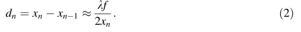

Fig. 1 (Color online) a Schematic diagram of the tilted MLL,b efficiency versus depth of the MLL along the optical axis, and c layer position. The calculated optimal efficiency of the 17.2 μm-MLL was 43.7% at tilted angle of 3.2 mrad at 10 keV
The MLL used within this study was designed at 10 keV using alternate target sputtering of WSi2and Si on a substrate. The one-dimensional diffraction effect is calculated using the dynamics theory of X-ray diffraction. This was first used by Takagi and Taupin (Diffraction, TTD) to describe the wavefront change of X-rays propagating when a crystal is distorted. In 2007, Yan et al. made some transplants and changes to the TTD theory, and used it to describe the propagation of X-rays in an MLL. After simplification,the wave field E of the MLL exit surface can be expressed as follows [6]:

where β represents the degree of deviation from the Bragg condition, θ is the incident angle of the plane wave X-ray,and h represents the diffraction order. Given the boundary conditions of the MLL, the partial differential equations can be solved, and the distribution of diffracted waves of different orders at different waveband positions and different depths of light can be obtained when X-rays propagate in the MLL. A variation curve of efficiency with the depth along the optical axis and layer position is shown in Fig. 1. The tilt angle affects the layer position of the tilted MLL to satisfy the diffraction dynamics, thereby affecting the focused spot and the diffraction efficiency. The range of the tilt angle is usually on the order of millimeter radians. As shown in Fig. 1b, the optimal tilt angle of the MLL is 3.2 mrad. When the tilt angle changes by 1mrad,the diffraction efficiency will decrease by approximately 10%.The most efficient layer position is approximately 0.7 times the total thickness, therefore, the tilt angle should be also approximately 0.7 times the outermost diffraction angle,as shown in Fig.1c.By optimizing the tilt angle,the optimum depth along the optical axis was determined to be approximately 7.5 μm. Following the above analysis, the calculated optimal efficiency of the 17.2 μm-MLL was 43.7% at tilted angle of 3.2 mrad at 10 keV.
3 MLL deposition
The multilayer was deposited onto a super-polished silicon substrate using a DC magnetron sputtering machine with a 4-inch target. The base pressure was below 2.0 × 10⁻⁴Pa before deposition, and Argon was used as the working gas with a pressure of 0.6 Pa, considering the factors of interface roughness and film stress.The working gas used during deposition was high-purity Ar gas(99.99%). The substrates used in the experiments were all single-sided polished Si (100) substrates with a roughness below 0.3 nm and a thickness of approximately 0.6 mm.In order to ensure the stability of film thickness, stress,roughness, as well as other factors, WSi2and Si were selected as the material combination for the preparation of MLL within this study due to their relatively small stress[11] and interface roughness [24]. The power of the WSi2target was 40 W, while that of the Si target was 80 W.
The layer thicknesses range of the designed MLL was varied from 7.2 to 36.1 nm. Several fixed individual thicknesses within the range were selected to process periodic multilayers to calculate the relationship between periodical thickness and deposition time. In this study, we used the X-ray diffractometer (XRD) produced by PANalytical to perform the GIXRR test of the periodic multilayer film samples prepared during the MLL rate calibration.The XRD is mainly composed of three modules: the light source, five-axis sample stage, and detector. X-rays are produced by electrons accelerated by a high-voltage electric field and hit a Cu target. After passing through a monochromator,slit,and collimating mirror,an X-ray with a wavelength of 0.154 nm and photon energy of 8.054 keV can be obtained. The multilayer film sample is placed on the sample stage, the translation of the sample stage is adjusted so that the light source illuminates the center of the sample and is in the half-cut position, and the rotation stage is scanned to maximize the light intensity. The reflectivity curve of the periodic multilayer was measured by the θ-θ scan mode,i.e.,the sample position is fixed and the angles of the light source and detector are increased.The fitting calculations of GIXRR curves were carried out to determine structural information about the multilayers,including thickness and interface roughness [25]. Table 1 shows the result of the d-spacing and individual layer thickness and roughness by fitting the measured GIXRR data.
The relationship between d-spacing (D) and time coefficient (t) is shown in Fig. 2. When t was equal to 1, the sputtering time for WSi2and Si was 22 s and 21 s,respectively, to make the thickness ratio of the two materials nearly 1:1, because the deposition rates of the two materials are slightly different. The time coefficient represents the ratio of the deposition time of the two materials to that when t is equal to 1.Similarly,when t is equal to 2,the growth time of WSi2and Si was 44 s and 42 s,respectively. The linear fit equation is D = 18.25t + 2.16.In the linear equation,the slope represents the growing rate of d-spacing, corresponding to the time coefficient, while the intercept represents the thickness when the substrate is moved back and forth above each target material.
For the preparation of the MLL, accurate control of the deposition rate calibration over a long period of time(dozens of hours)is crucial.Because magnetron sputtering is a target-consuming coating process,the deposition rate isbound to change as the target is used for longer periods of time. This problem exists in both high energy resolution multilayers and Laue-type multilayers, so the sputtering environment must be kept as stable as possible, and the sputter rate drift should be considered and corrected.

Table 1 D-spacing, individual layer thickness, roughness, and time coefficient of each multilayer
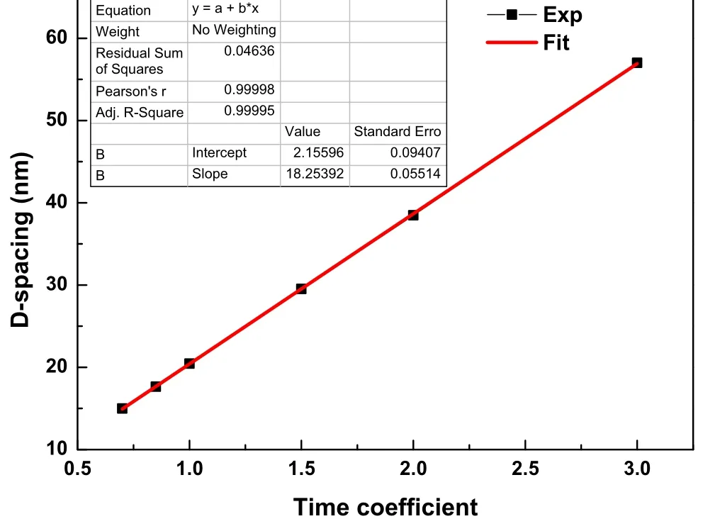
Fig. 2 D-spacing of WSi2/Si distribution obtained from periodic multilayers,where the relationship between the d-spacing(D)and the time coefficient (t) is D = 18.25t + 2.16
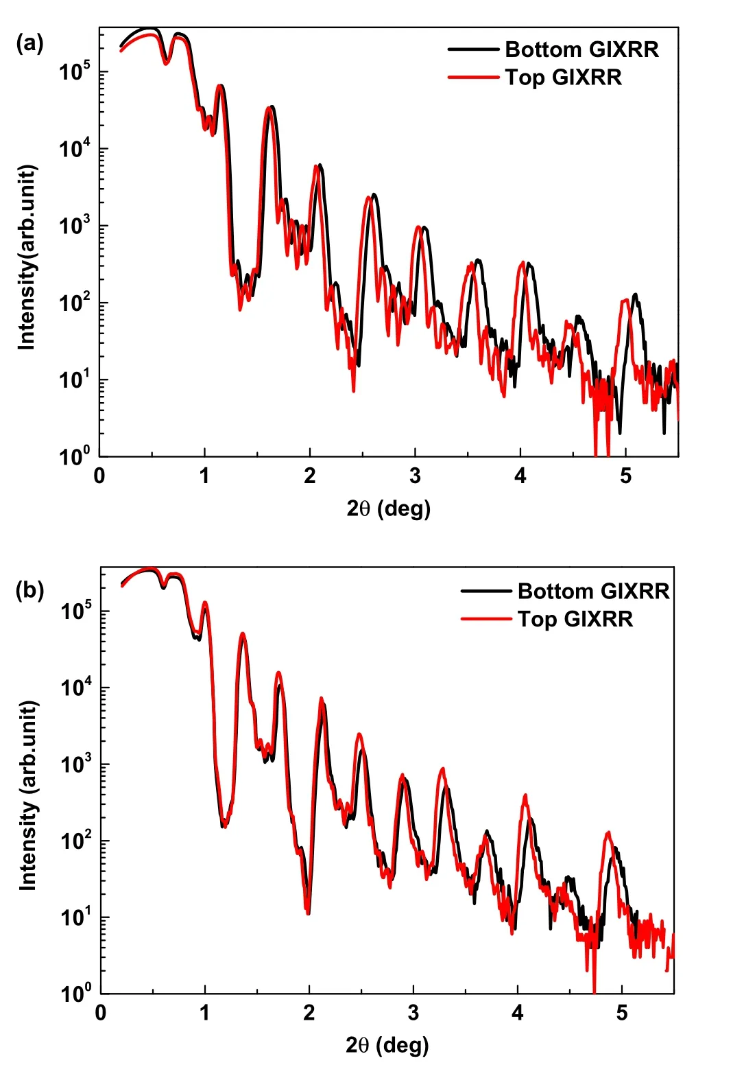
Fig. 3 (Color online) The change in periodic thicknesses measured by GIXRR a before and b after correction, where the long-term growth rate drift was corrected from 2 to 0.6%
Because the amount of target material will be decreased during the sputtering time, the sputtering rate will change accordingly. The layer deposition accuracy will be improved through the calibration sputtering rate at the sputtering time. The total coating time of the 17 μm-MLL is approximately 48 h. Therefore, we prepare periodic multilayers with the same coating parameters on the bottom and top of the MLL,with a d-spacing of approximately 20 nm. The periodic thicknesses are measured by GIXRR before and after correction, as shown in Fig. 3. The result presents a series of sharp Bragg peaks corresponding to different diffraction orders from the multilayer structure.This demonstrates that the film quality of the multilayer did not change significantly during the 48 h coating process.The periodic thickness of the multilayer film can be obtained by fitting the top and bottom GIXRR curves.The initial periodic thickness error between the top and bottom of the MLL was 2%,as shown in Fig. 3a,and the long-term coating resulted in a faster film deposition rate. We assumed that the drift of the sputtering rate had a slow linear change because the formation and deepening of the etch ring of the target was also slow,and subsequently,we added the rate correction. The Bragg diffraction peaks of the first five orders were essentially coincident,as shown in Fig. 3b.After the curve fitting,the periodic thickness error was reduced to 0.6%. The d-spacing calculated from the GIXRR curve was used to calibrate the d-spacing measurement error caused by the non-perpendicular crosssections of the multilayer film and the electron beam during the SEM test.
4 Lens fabrication
The incident X-ray energy determines the lens depth along the optical axis to achieve the best efficiency of high numerical aperture focusing. For the MLL designed in Sect. 2, the optimal depth was determined to be approximately 7.5 μm at 10 keV. In order to precisely control the depth of the lens and to achieve high-quality fine polishing of the entrance and exit surfaces, we used the semiconductor processing technology as a reference, such as photolithography masks, RIE, dicing, and FIB polishing.
Before the MLL etching, a mask pattern should be formed on the upper surface of the MLL to shield the etching of the ion beam, and the mask is formed with a photoresist material. This study draws on part of the process and technology of lithography. Lithography is mainly conducted under the action of light with a wavelength that is generally within the ultraviolet or extreme ultraviolet band,and the pattern on the mask plate is transferred to the substrate. The main process is as follows: first, a layer of photoresist is deposited on the surface of the multilayer;light is then irradiated to the surface through the mask,and when the photoresist selects the positive photoresist and the pattern of the mask is consistent with the pattern on the film, the photoresist in the exposed area undergoes a chemical reaction due to light exposure; the photoresist in the exposed area is dissolved and removed by developing so that the mask is retained on the MLL samples.
RIE is used to etch away the entire film,leaving only the mask portion. RIE is a relatively advanced dry etching technology that has arisen in recent years. The traditional wet etching method produces poor quality after etching due to the isotropy of the etching material,and the mask cannot be completely shielded. RIE is an anisotropic etching, and the etching rate and precision are flexible and controllable.It has become an effective method for etching micron or even nanometer patterns. The core principle of RIE is to pass a reactive gas between the plate electrodes, and to ionize the gas by applying a radiofrequency voltage. The generated plasma induces both chemical etching and physical bombardment on the sample. In the experiment,the combined reaction gas of O2and SF6was used,and the etching height was measured by a step profiler (Bruker Dektak XT).In order to prevent the photoresist from being consumed by the excessive etching of gas ions, we attempted to increase the thickness of the photoresist as much as possible,and simultaneously optimize the etching process to decrease the etching ratio of the photoresist to the thin film material. After each etching process, the shielding of the photoresist on the upper surface of the film was observed by an SEM (Hitachi S-4800),and finally the MLL etching result with a depth of more than 20 μm was achieved.
Because the working distance of the MLL is very small(on the mm-scale), a dicing machine was used to cut and separate the samples after RIE. The dicing machine is a precise numerical control equipment that integrates technologies such as air spindle, precision mechanical transmission, and sensor and automatic control. By optimizing the blade type,thickness,and cutting speed,the MLL is cut into sizes of 2 mm × 1 mm with almost no edge chipping.The 2-mm-long side was used for nanometer experiments to be parallel to the sample stage, and the 1-mm-long side was used for transmission focusing experiments. At present, a 10 mm × 10 mm multilayer can be separated into at least 30 individual lenses for subsequent processing.
The final process of lens fabrication is FIB.The purpose is to further thin the lens after RIE to the depth along the optical axis that satisfies the diffraction dynamics. It is simultaneously necessary to use FIB to finely polish the entrance and exit surfaces of the MLL to improve the surface roughness and to reduce scattering of X-rays. FIB is a cutting and polishing technology that focuses the ion beam into a very small size, with auxiliary functions such as imaging and coating. Ion beams are mostly drawn from liquid metal ion sources, and gallium ion sources with a low melting point and low vapor pressure are generally selected. The size of the ion beam is varied by a series of lenses with variable apertures, and the desired ion species are then selected. Finally, the ion beam is focused by a deflection device and an objective lens, which can be used for ion beam sputtering coating, or cutting or polishing.The generated secondary electrons and ions are collected and the surface information of the sample can be observed.When cutting with the ion beam, the image will be observed with the electron beam to characterize the quality of the lens manufacturing online. To optimize the etching beam,the process of chemical mechanical polishing(CMP)is used for reference,that is,a large ion beam(~100 nA)is used to thin a large area during the etching process, and the beam is gradually reduced during the polishing process to achieve precision polishing for enhanced processing efficiency and quality.The top and side view of final lens is shown in Fig. 4. The length and width of the MLL was approximately 100 μm and 17.2 μm, respectively, while the depth along optical axis was approximately 7.5 μm. It is clear from the SEM image that the FIB does not damage the structure of the multilayer film, and the film information remains intact. The white horizontal stripes in Fig. 4b represent the symbol layers,where the space between each symbol is approximately 1 micron in order to stitch the SEM figure in both high and same magnifications to measure the actual thickness of each layer. The accumulated layer position error was 4.15 nm (rms), which has been described in detail elsewhere [22].
5 Focusing measurement
To date,various focusing optics utilizing total reflection,Bragg diffraction,and refraction have successfully focused hard X-rays to sizes on the order of tens of nanometers.The direct measurement methods applied to the nanoscale focusing spot mainly include fluorescence knife edge scanning and fluorescence nanowire scanning. The principle is to generate fluorescence through a fluorescent film(usually Cu, Ni, etc.). The unevenness of the fluorescent knife edge will cause the focused spot to be broadened,which is not suitable for the measurement of small spots,but the diffraction efficiency can be measured. The fluorescence scanning nanowires prepared by magnetron sputtering coating technology and subsequent thinning and polishing technologies can have very high smoothness and are suitable for the measurement of focused spots of tens of nanometers to several nanometers.
In this study, a new preparation method of fluorescent scanning nanowires was designed, which was prepared by a series of non-contact processing methods, such as magnetron sputtering, ion beam etching (IBE), and FIB polishing technology,which is similar to the fabrication of the MLL in Sect. 4.The preparation method of this fluorescent nanowire first utilizes magnetron sputtering to deposit a fluorescent film on the substrate with a thickness of 5 nm,which has very little influence on the broadening effect of the nano-focusing spot. The method then involves IBE to etch the fluorescent film and substrate to a depth of ~20 μm, uses the ion beam sputtering deposition (IBSD)method to coat a protective layer on the fluorescent film,uses the FIB method to thin the fluorescent film to a depth of 5 μm along the optical axis, and achieves double-sided polishing by continuously reducing the processing ion beam current. The length and width are approximately 100 μm and 20 μm, respectively. With high precision and less stress,the film will not fall off and be damaged during preparation, installation, or testing. More importantly, this fluorescence scanning nanowire is independently supported on the substrate,which can be directly fixed on the sample stage, so X-rays can penetrate the nanowire and image in the far-field scintillator which can be easily adjusted, as shown in Fig. 5b. Consequently, the difficulty regarding the relative positioning and posture of the nanowire and the MLL is reduced. The depth along the incident X-ray direction is smaller than the focus depth of the MLL(~60 μm),thus avoiding the broadening of the focus spot.At present, no similar preparation method has been established.

Fig.4 a Top and b side view of the MLL after lens fabricating by SEM,the length and width of the MLL is approximately 100 μm and 17.2 μm,respectively, while the depth along optical axis is approximately 7.5 μm

Fig. 5 a Nano-focusing experimental device at BL15U1, SSRF and b image of the MLL and nanowire on the far-field scintillator from the synchrotron radiation source
The nano-focusing experiment of the MLL began at the Shanghai Synchrotron Radiation Facility (SSRF) BL15U1 with an undulator as the insert device.X rays pass through a water-cooled four-knife slit to limit the receiving angle.The toroidal mirror is used to focus to a ratio of 2:1 in the horizontal direction, and the vertical direction is collimated. At 10 keV, the energy resolution can reach 1.5 × 10⁻⁴by a Si (111) double crystal monochromator(DCM). The monochromaticity (temporal coherence) satisfies the requirement. A diffraction-limited focused spot can only be obtained if the optimal coherence condition is satisfied.The secondary slits are placed 33.8 m away from the light source. At the experimental station, the incident beam size is shaped by a four-knife slit to a size of 17 μm × 100 μm (V × H). The experimental device of the nano-focusing test is shown in Fig. 5. The MLL is mounted on the 3D rotation and translation stages, and are focused in the vertical direction because the incident beam demonstrates a better spatial coherence in this direction.One of the most important factors here is to adjust the Bragg angle of the MLL to maximize the diffraction efficiency.The fluorescent nanowire and knife are mounted on the sample stage,including 3D translation,1D rotation,and the nanostage. The rotation stage can ensure the nanowire and MLL are parallel, the translation stage is used to find the focus, and the nanostage can accurately scan out the distribution of the spot.
In the test experiment,a laser interferometer was used to determine the positional accuracy of the MLL stage and sample stage.A scintillator,placed at a far-field diffraction position of approximately 1 m to several meters, was used to measure the diffraction pattern at each position and posture of the MLL and flourescent nanowire.Considering that this method is very sensitive to the movement of the position,there was a large number of moving steps,a long experimental time for collecting the diffraction pattern,and an extremely high stability of the system was required[26],which was ensured at approximately 0.05 °C. For fluorescence scanning, a silicon drift detector (SDD) was used,which was placed at a position 90 degrees from the straight through light. A fluorescent nanowire made of an Ni film with a width of 5 nm and depth of 10 μm was used to measure the spot size, while the Ni knife edge was used to measure the diffraction efficiency. In terms of angle adjustment, the projection angle was determined by observing the change in the light intensity of the diffraction spot of the scintillator and the distribution of the spot. The swing angle was judged by observing whether the MLL and the flourescent nanowire coincided,because the length dimensions of the two were equal.The relative roll angle of MLL and nanowires were the most important factor causing the broadening of the focus spot.This was observed on the scintilator whether the upper edges of the two were completely coincident or not, because the scintillator was far away from the MLL, which is equivalent to the projected image having been enlarged dozens of times,so that the adjustment accuracy is relatively high.
The intensity of Ni Kα was monitored by an X-ray fluorescence detector. The nanowire as placed at the focal point of the MLL(~3 mm away from the MLL),and the scanning step of the nanostage was 20 nm. First, the approximate position of the focus was determined by rough scanning of the nanowire, and two-dimensional mapping was subsequently conducted to accurately determine the focus position. The one-dimensional focused spot size at the focal point was 64 nm, as shown in Fig. 6a. The knife edge was placed close to the exit surface of the MLL, and this scanned from the outermost layer to the innermost layer of the MLL,so that it first passed through the through light, and then passed through the -1st-order diffracted light.The diffraction efficiency was determined to be 38%,as shown in Fig. 6b, which was close to the theoretical calculation of 43.7%, but the focused spot had a certainbroadening. The reason may be that the relative posture of the nanowire and MLL was not optimally adjusted. The cumulative film position error of the MLL, the relative vibration of the MLL stage and the sample stage, and the high frequency position vibration of the incident beam can also broaden the spot.
Fig. 6 (Color online) a Fluorescence intensity distribution measured by the nanowire at the focal spot and b knife edge near the exit surface of the MLL. The one-dimensional focused spot size was 64 nm, while the diffraction efficiency was 38%
6 Conclusion
In this paper,the diffraction properties of the MLL were calculated. A multilayer structure consisting of a total of 1736 layers with a 7.2 nm outermost layer and a total thickness of 17 μm was prepared using a DC magnetron sputtering machine.The sputtering rate of WSi2and Si and the rate drift of long-term coating were calibrated using the multilayer deposited on the bottom and top of the MLL and the GIXRR measurement. The lens which met the requirements of diffraction dynamics was fabricated using photolithography masks, RIE, dicing, and FIB polishing.The focusing resolution and diffraction efficiency of the MLL were tested at the SSRF BL15U and the MLL vertical focusing spot was scanned using a fluorescent nanowire and knife edge. At a photon energy of 10 keV, the onedimensional line focusing resolution of MLL was 64 nm,and the diffraction efficiency of the -1st order was 38%.This is the best nanometer focusing result in the hard X-ray field in China. Further effort will be made to improve the fabrication process, the experimental system, and methods such as ptychography, in order to further increase the resolution of the MLL.
AcknowledgementsThe authors thank Ai-Guo li, Hui Jiang, Hua Wang, Shuai Yan, Dong-Xu Liang from SSRF BL15U for their technical support.
杂志排行

Nuclear Science and Techniques的其它文章
- Monte Carlo study of the neutron ambient dose equivalent at the heavy ion medical machine in Wuwei
- Experimental investigation on the characteristics of molten lead–bismuth non-eutectic alloy fragmentation in water
- Configurational information entropy analysis of fragment mass cross distributions to determine the neutron skin thickness of projectile nuclei
- Differences in MBUs induced by high-energy and medium-energy heavy ions in 28 nm FPGAs
- Thin-film approximate point scattered function and its application to neutron radiography
- Mechanical properties and surface characteristics of SiC fibers irradiated by swift heavy ions