Physical analysis of normally-off ALD Al2O3/GaN MOSFET with different substrates using self-terminating thermal oxidation-assisted wet etching technique
2022-09-24ChengYuHuang黄成玉JinYanWang王金延BinZhang张斌ZhenFu付振FangLiu刘芳MaoJunWang王茂俊MengJunLi李梦军XinWang王鑫ChenWang汪晨JiaYinHe何佳音andYanDongHe何燕冬
Cheng-Yu Huang(黄成玉) Jin-Yan Wang(王金延) Bin Zhang(张斌) Zhen Fu(付振)Fang Liu(刘芳) Mao-Jun Wang(王茂俊) Meng-Jun Li(李梦军) Xin Wang(王鑫)Chen Wang(汪晨) Jia-Yin He(何佳音) and Yan-Dong He(何燕冬)
1School of Integrated Circuits,Peking University,Beijing 100871,China
2Beijing Chip Identification Technology Co.,Ltd,Beijing 102200,China
Keywords: atomic layer deposition Al2O3/GaN MOSFET, normally-off, interface/border traps, thermal oxidation-assisted wet etching
1. Introduction
GaN, as wide band gap semiconductor material, has a bright future in the field of power semiconductor devices due to its advantages of high thermal conductivity, high breakdown electric field, and high electron saturation drift velocity. Two-dimensional electron gas(2DEG)with high concentration and high mobility can be formed at the AlGaN/GaN interface due to the strong polarization effect in III-nitrides.However, the traditional AlGaN/GaN high electron mobility transistor (HEMT) is a depletion-mode device, Considering the design of driving circuit. single polar power supply, and the safe operation,it is necessary to realize enhancement mode(E-mode)AlGaN/GaN device. Various techniques have been proposed to realize the normally-off operation of AlGaN/GaN HEMTs.[1-4]Among them, the recessed-gate with insulator gate dielectric is a commonly used structure to realize E-mode GaN device because of its high gate voltage swing, low gate leakage current, and high threshold voltage, which has been widely studied for realizing E-mode GaN HEMTs.[4]
Our research group has developed a self-terminating thermal oxidation-assisted wet etching technique[5]to realize the E-mode MOSFET structure,the device which is simple to fabricate, easy to control, and possesses reliable performance,has broad market prospects. In this work, based on this technique,the enhancement mode Al2O3/GaN MOSFETs of sapphire substrate and Si substrate were developed, respectively.And the characteristics of the two devices were analyzed.The indicators reflecting the significant improvement in the sapphire substrate device are maximum drain current (Idmax),field-effect mobility (µFEmax), and on-state resistance (Ron).The experimental results show that the difference in device performance depends on the difference in Al2O3/GaN interface state. The interface/border trap density in the Si substrate device is one order of magnitude higher than that in the sapphire substrate device. The border traps in Al2O3dielectric and the interface traps in Al2O3/GaN gave a significant effect on device channel mobility. The quality of GaN grown on Si is not so good as that grown on sapphire.
2. Device fabrication
2.1. Sapphire substrate device
The AlGaN/GaN epitaxial structure studied here were grown on a 3-in(0 0 0 1)sapphire substrate by metal organic chemical vapor deposition(MOCVD)(1 in=2.54 cm). In the AlGaN/GaN epitaxial structure, the GaN buffer layer is 1.5-µm thick, GaN channel layer is 120-nm thick, AlN spacer layer is 1-nm thick,Al0.23Ga0.77N barrier layer is 18-nm thick,and GaN cap layer is 2-nm thick. Its structure is shown in Fig.1(a).
2.2. Si substrate device
The epitaxial structure studied here was grown on a 3-in p-type(111)Si substrate by metal-organic chemical vapor deposition (MOCVD). In the epitaxial structure, GaN buffer layer is 1.5-µm thick,GaN channel layer is 120-nm thick,AlN spacer layer is 1-nm thick, Al0.23Ga0.77N barrier layer is 25-nm thick, and GaN cap layer is 2-nm thick. Its structure is shown in Fig.1(b).
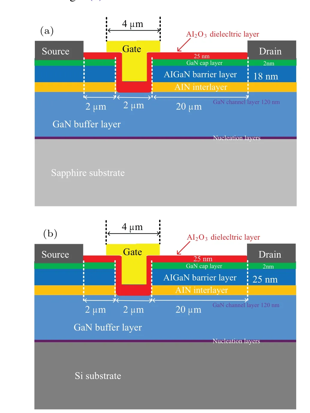
Fig.1. Structure diagram of GaN MOSFET with 25-nm-thick ALD Al2O3,showing(a)sapphire substrate GaN MOSFET with ALD Al2O3 and(b)Si substrate GaN MOSFET with ALD Al2O3.
Self-terminating thermal oxidation assisted wet etching technique process flows of these two devices were identical.First, the fabrication of devices started with gated recess fabrication, GaN cap layer served as a recess mask.[6]Specifically,650-°C thermal oxidation lasted 50 min,and then 70-°C wet etching in KOH rtook 75 min. And then at 250°C, 18-nm or 25-nm-thick gate dielectric Al2O3layer was deposited by atomic layer deposition(ALD).After removing the dielectric Al2O3at the source and drain positions by buffered oxide etch, Ohmic contact Ti/Al/Ni/Au (20/160/50/100 nm) metal stack was fabricated by e-beam evaporation. Then at 870°C,rapid thermal annealing lasted 30 s. Then,multi-energy F-ion implantation for device isolation was conducted. Finally, a gate region was defined by the lithography technique,and the Ni/Au gate stack was completed by e-beam evaporation.
3. Results and discussion
TheID-(VGS-Vth)andID-VDScharacteristics of the GaN MOSFETs with sapphire substrate and Si substrate are shown in Fig.2. The geometrical dimensions of both samples are as follows. A gate-source distanceLGSis 2 µm, a gate lengthLGis 2 µm, a gate-drain distanceLGDis 20 µm, and a gate widthWGis 20 µm. Figure 2(a) shows the transfer characteristics of the GaN MOSFETs with sapphire substrate device and Si substrate device atVds=7 V.TheVgsvoltage increases from-2 V to 7 V for the sapphire substrate device,and from-2 V to 7.5 V for the Si substrate device. The threshold voltage (Vth) is 0.2 V for the sapphire substrate device and 1.5 V for the Si substrate device. The two devices are well pinched off atVGS=0 V.With the upward scanning of gate voltageVGS,drain currentIDof sapphire substrate device rises rapidly,indicating better gate control performance of sapphire substrate device. The maximum drain currentIdmaxis~401 mA/mm and the maximum transconductanceGmis~75 mS/mm for sapphire substrate device, while theIdmaxandGmare~228 mA/mm and~55 mS/mm for the Si substrate device. Thus,it can be seen that comparing with the Si substrate device,the maximum drain current of sapphire substrate device is 1.76 times that of silicon substrate device. The output characteristics of the sapphire substrate device and Si substrate device withVGSscanning from 0 V to 8 V in steps of 2 V are shown in Fig. 2(b). The performance of sapphire substrate device is improved obviously. UnderVGS=8 V andVDS=10 V bias, GaN MOSFET of sapphire substrate has a very high drain current (401 mA/mm), and a very small onresistance(15.2 Ω·mm),in comparison with the the maximum drain current of 228 mA/mm and on-resistance of 21.2 Ω·mm of the Si substrate device.
It is obvious that the performance of the sapphire substrate device is better than that of Si substrate device. The difference in performance between the sapphire substrate device and Si substrate device is very large. In order to analyze its underlying mechanism, we evaluate the interface trap distribution of the GaN MOSFET with ALD Al2O3gate dielectric by the conductance method.[7]This technique is based on measuring the equivalent parallel conductanceGpof an MOS capacitor as a function of bias voltage and frequency. The MOS capacitor equivalent circuit is shown in Fig.3(a),where theCoxrepresents the capacitance of the gate insulator,andCsrefers to the capacitance of the channel depletion region. TheCitandRitin series describe the capacitance effect of the traps located at the interface between the gate insulator and the GaN buffer layer. TheRittogether with theCitdescribes the time delay(τit)required for the electrons trapped at the interface to form an equilibrium with those in the channel,τit=RitCitbeing the time constant of interface trap,andCitbeing related to the trap density(Dit). Simplified circuit of Fig.3(a)is shown Fig.3(b),whereCpandGpare the equivalent parallel capacitance and conductance respectively.
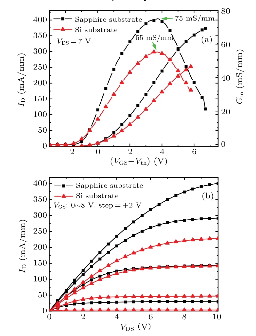
Fig.2. The I-V characteristics of the fabricated GaN MOSFET with device dimension of LGS/LG/LGD/WG=2/2/20/20µm: (a)transfer characteristics and(b)output characteristics.
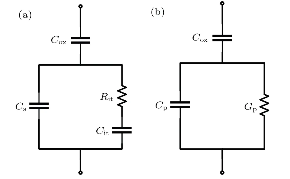
Fig.3. (a)Equivalent circuit of MOS capacitor with interface trap,and(b)simplified circuit of equivalent circuits of MOS capacitor with interface trap,with Cp and Gp denoting equivalent parallel capacitance and conductance respectively.
Figure 4 shows the curves ofGp/ω versus ωunder differentVgsfor sapphire substrate device and Si substrate device,
whereGp/ωnamed the normalized equivalent parallel conductance is the frequency-dependent values ofGpand can be used to calculate the interface trap density,andωis the angular frequency. The measured capacitance and conductance are used to extract the normalized equivalent parallel conductance(Gp/ω). By assuming a single trap level, the relationship ofGp/ω versus ωcan be given below:

Thefscanning frequencytranges from 1 kHz to 1 MHz in the experiment, the gate bias voltage scanning ranges from-0.5 V to 0.1 V and from 0.8 V to 1.4 V in steps of 0.1 V for the sapphire substrate device and Si substrate device, respectively. The MOS capacitor is biased at the depletion state so that the Fermi level is located within the GaN bandgap for the detection of interface traps. As can be seen from Fig. 4,the peak value ofGp/ωmoves towards high frequency as the bias increases.[8-15]It has similar characteristics to other existing reports. But theGp/ωvalue of Si substrate device is significantly higher than that of sapphire substrate device. For sapphire substrate device, theGp/ωvalue is small when the frequency is below 105s-1, instead,Gp/ωvalue of Si substrate device is still large. Indicating that the deeper level trap of Si substrate device is higher than that of sapphire substrate device.

Fig. 4. Characteristics curves Gp/ω versus ω of MOS capacitor for (a)sapphire substrate device bias (from -0.5 V to 0.1 V in steps of 0.1 V)and (b) Si substrate device at bias (from 0.8 V to 1.4 V in steps of 0.1 V).Gp/ω is normalized equivalent parallel conductance,with ω being angular frequency.
As can be seen from Fig.4,the curve obviously has more than one peak value, and the equivalent parallel conductivity model of single-level trap cannot be applied to our system.Hence, in order to quantitatively extract the interface states,theGp/ωcurves are fitted through considering two or three different distributions of trap density levelsDitwith different values of time constantτitby using the following equations:[7]

whereω=2π fis the radial frequency,Dit1,Dit2,andDit3are the interface trap densities,τit1,τit2,τit3are the time constants of traps. Figure 5 show the experimental and fitting curves of MOS capacitor with sapphire substrate and Si substrate at bias voltages of-0.2 V and 0.9 V,the measurement curves and fitting curves of the two MOS devices are in good consistency with each other. For devices of sapphire substrate,each measured curve can be decomposed into two fitting curves,showing that there are two types of traps at a given bias voltage.For Si substrate device,each measured curve can be decomposed into three fitting curves. It can be seen from Fig.5 that there are at least two peak values in theGp/ωcurve of sapphire substrate device, and at least three peak values in theGp/ωcurve of Si substrate device. TheDitof traps is a function of trap characteristic time constant (τit) and trap energy level as shown in Fig.6. The relationship between the time constants and trap energy level is expressed as

wherevth= 2.6×107cm/s is the thermal velocity,Nc=2.7×1018cm-3is the effective density states in the GaN conduction band,[15]andσn=1×10-14cm2is the electron capture cross section.
In Fig. 6, There are two kinds of traps that are continuous distributions of energy level ranging from 0.34 eV to 0.41 eV and from 0.42 eV to 0.46 eV. Both traps should be attributed to common interface states,[10]marked as interface trap in Fig. 6. And the other kinds of traps are very possible to be border trap states, for they exhibit single trap energy level of around 0.48 eV,marked as border trap in Fig.6.Note that the time constant of a border trap is~1.5×10⁻⁴s,which is close to our extraction value~1.8×10⁻⁴s reported at Al2O3/GaN interface.[13]Moreover, what is observed at SiO2/GaN interface[14,15]is also a similar border trap with a time constant of~1.4×10⁻⁴s-3×10⁻⁴s. Figure 6 shows the curves of interface trap and border trap extracted from sapphire substrate and Si substrate MOS capacitors, and the increase of measured trap density withVGSincreasing,indicating the apparent differences in trap distribution and density.First, the interface trap concentration of Si substrate device with energy distribution between 0.34 eV and 0.41 eV is nearly one order of magnitude higher than that of sapphire substrate device. The Si substrate device has a wide interface trap distribution,while the sapphire substrate device has no interface trap distribution between 0.4 eV and 0.46 eV. Furthermore,the border trap concentration of Si substrate device is one order of magnitude higher than that of sapphire substrate device.It shows that the quality of GaN grown on Si is inferior to that grown on sapphire substrate.which is likely to be due to the fact that the GaN grown on Si substrate has higher oxygen and nitrogen vacancies.[13,17-20]
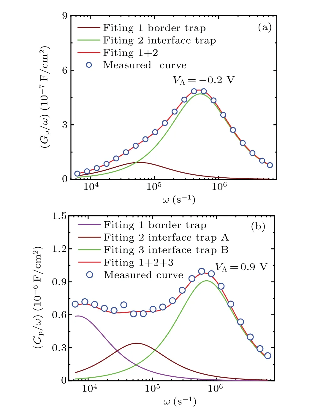
Fig.5.Measured curves and fitting curves of Gp/ω versus ω at VA of-0.2 V and 0.9 V for(a)sapphire substrate device and(b)Si substrate device.

Fig.6. Trap state density as a function of energy level for both devices.
It can be seen from Fig.7 that with the gate bias increasing,Si substrate MOS capacitor increases continually and the sapphire substrate MOS capacitor trends to saturate. Therefore,it can be reasonably inferred that the degraded transport performance in the channel of Si substrate device can be attributed to the presence of high density of interface traps and border traps at the Al2O3/GaN interface. The Al2O3/GaN MOS capacitor structure with interface trap and border trap distributions is shown in Fig.8.
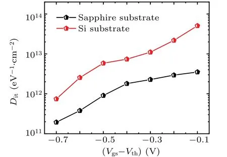
Fig.7. Curves of trap state density of border trap versus Vgs-Vth.
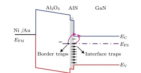
Fig. 8. Schematic band diagram of Al2O3/GaN MOS capacitor structure with interface trap and border trap distributions.
In addition,the field effect mobility at low field(µFE)for the sapphire substrate device and the Si substrate device are also extracted in the linear region (Vds=0.1 V) and shown in Fig. 9. When a GaN MIS HEMT device operates in a linear operating region, the drain currentIDScan be expressed as[6,21,22]
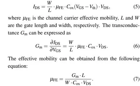
From Eq. (7), the maximum field effect mobility (µFEmax) is calculated to be 176 cm2/V·s for sapphire substrate device and 96 cm2/V·s for Si substrate device. The accumulation capacitance (Cox) is 378 nF/cm2for sapphire substrate and 386 nF/cm2for Si substrate.

Fig. 9. Curve of extracted field effect mobility (µFE) versus VGS-Vth for sapphire substrate device and for Si substrate device.
Some authors described the channel mobility on MOSFETs fabricated by wide bandgap semiconductor,[23-26]with consideration of the contributions to the Matthiessen’s rule,made by the bulk mobility factor (µB), the acoustic-phonon scattering (µAC), the surface roughness scattering (µSR), and the Coulomb scattering (µC) due to the presence of interface charges,specifically

The study of the temperature behavior of the field-effect mobility is a useful method to acquire the information on the insulator/semiconductor interface properties in MOSFETs. Figure 10 shows the experimental results of the field-effect mobilityversus VG-Vthat different measured temperatures(298 K-398 K).As can be seen,the maximum values of these curves decrease as the measured temperature increases.
Figure 11 shows the peak of the field-effect mobility values as a function of temperature, extracted from Fig. 10. As can be seen, the experimental peak mobility values decrease with the measured temperature increasing. As can be seen from Eq.(8),the limiting factor of the mobility comes from the contributions made by the surface roughness(µSR),the acoustic phonon (µAC), and the Coulomb scattering (µC) contributions.Because the larger value of bulk mobility only has a negligible effect on the total mobility. The sapphire substrate device is mainly responsible for acoustic-phonon scattering,and Si substrate device is mainly responsible for the surface roughness scattering. It should be mentioned that the subthreshold region of theIDS-VDScan be affected by the non-steep change in the gate capacitance. The early ascending part of the curve of field-effect mobilityversusVGS-Vthcan be influenced by the soft gate-capacitance variation. However, forVGS-Vth>1 V the device is in accumulation and the capacitance value is almost constant. Hence, the peak mobility values used in the following are not affect by the capacitance value variation.
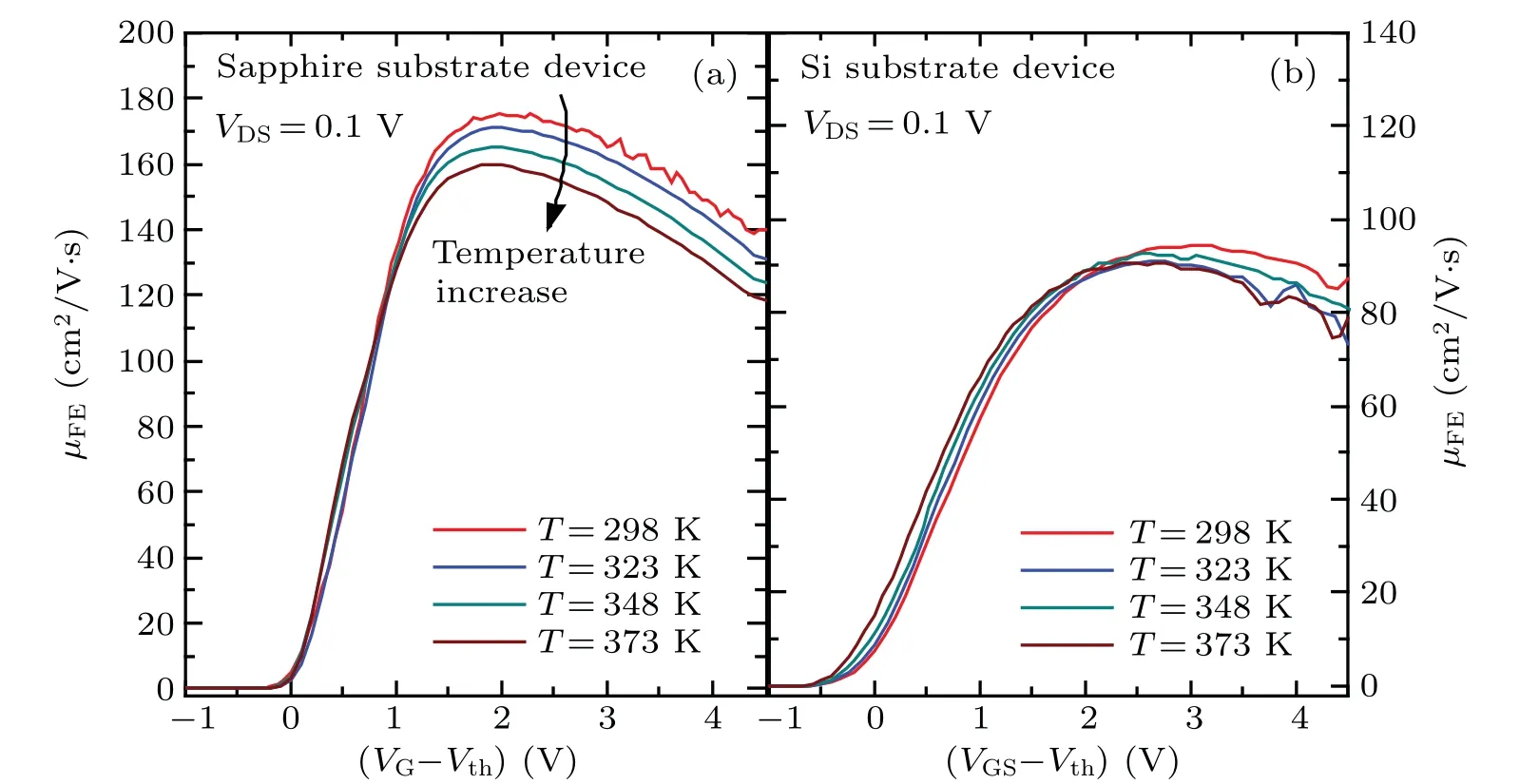
Fig.10. Curves of field-effect mobility(µFE)versus VG-Vth at different temperatures for(a)sapphire substrate device and(b)Si substrate device.
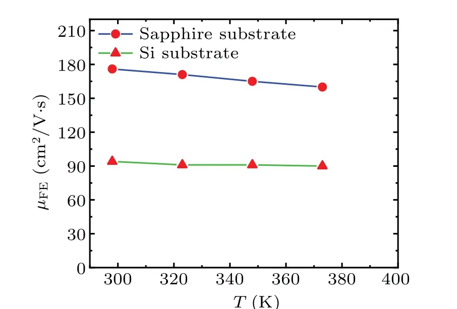
Fig.11. Peaks of the field-effect mobility values as a function of temperature.
Figure 12 displays the temperature-dependentC-Vmeasurement results for GaN MOSFET with sapphire substrate and Si substrate, respectively, showing that our model reproduces the characteristic shapes ofC-Vcurves from the MOS capacitors,specifically,a nearly flat part of the voltage above threshold voltage (Vth), a rapid change in the capacitance atVth, and a very small capacitance in the subthreshold region(belowVth). The capacitance for the gate voltage of the voltage above threshold voltage(Vth)is determined by the capacitance of Al2O3layer and is almost bias-independent. The capacitance in the subthreshold region depends on the background doping in the GaN layer. The effect of increasing temperature onC-Vcurve is a reduction of the slope caused by the increased Debye length and the thermal broadening of the Fermi-Dirac distribution.[27]The slope of sapphire substrate device,KSapphire,is greater than that of Si substrate device,KSias shown in Fig. 12. The higher the trap concentration, the lower the slope is. It shows that the trap concentration of the interface of Si substrate device is higher that of sapphire substrate device.
On the other hand, the increasing in temperature led theC-Vcurves to shift positively by around 0.04 V for sapphire substrate device. But the increasing in temperature results in a negative shift ofC-Vcurves by around 0.2 V for Si substrate device as shown in Fig.13. The temperature-dependent voltage shift is attributed to the depletion and redistribution of carriers.[28]The negative shift of theC-Vcurve of the Si substrate device indicates that the shallow level trapped electrons are detrapping and a positive charge appears. The larger the trap charge concentration, the larger theVthshift is, indicating the excellent Al2O3/GaN interface quality for sapphire substrate device.
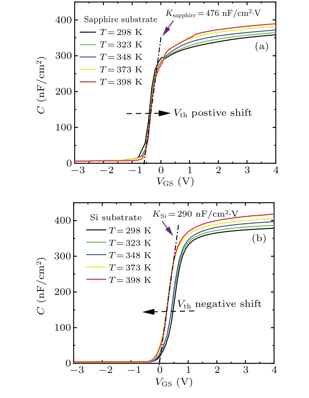
Fig. 12. The VGS-dependent gate capacitance for (a) sapphire substrate device and(b)Si substrate device at various temperatures.

Fig.13. The Vth shifts versus temperature for sapphire substrate and Si substrate.
To further study the crystalline quality of the GaN epilayers on sapphire substrate and Si substrate,the crystal quality of GaN is analyzed by high resolution x-ray diffraction measurements.The measurement results of symmetric(002)plane and asymmetric(102)plane of GaN epilayer are shown in Table 1.The full width at half maximum(FWHM)values of the(002)and(102)planes for the GaN of sapphire substrate are 316 arcsec and 613 arcsec,while those for the GaN of Si substrate are 688 arcsec and 941 arcsec respectively. The FWHM value of(002)plane for the GaN of Si substrate is about twice that for the GaN of sapphire substrate,and the FWHM value of(102)plane for the GaN of Si substrate is about one and a half times that for the GaN of sapphire substrate. Because the FWHM value is associated with threading dislocation density in GaN epilayer,this significant difference FWHM value confirms that quality of GaN of sapphire substrate is better than that of GaN of Si substrate.One of the biggest challenges is the large stress caused by the thermal mismatch between GaN epilayer and Si substrate.The large lattice mismatch between GaN and Si will result in high density dislocations. Owing to the existence of oxygen,silicon impurities and nitrogen vacancies,the quality of GaN grown on Si is not good.[29,30]

Table 1. X-ray diffraction measurement results of GaN epilayer on sapphire and Si.
By comparing the fabrication of the sapphire substrate device with the fabrication of the Si substrate device, it can be assumed that a self-terminating gate recess technique used for recessed GaN MOSFET fabrication can effectively inhibit the generation of interface and border trap at the Al2O3/GaN interface, thus improving the device performance. The selfterminating thermal oxidation assisted wet etching technique is shown to be effective and feasible. At the same time, the technique is also shown to cause different property changes in gallium nitride materials with different substrates. This finding can be used as a reference for further optimizing the Si substrate devices.
4. Conclusions
The improved GaN MOSFET device with sapphire and silicon substrates are developed based on our proposed the thermal oxidation-assisted self-terminating gate recess technique, and two kinds of devices are systematically studied.The experimental results demonstrate that the performance index of the enhanced device on sapphire substrate in terms ofIdmax(~76%),µFEmax(~83%) as well asRon(~39%) is significantly improved in comparison with that of the device on silicon substrate. Moreover,the frequency-dependent conductance measurement is used to evaluate the performance of the device. The results show that the improvement of the device performance on sapphire substrate should be attributed to the significant suppression of self-terminated groove gate technology that significantly inhibits the Al2O3/GaN interface and border trap,and reduces the time constant of interface trap to~1×10⁻⁶s-8×10⁻⁶s and the time constant of border trap to~1.6×10⁻⁴s-3×10⁻⁴s, respectively. Our experimental results demonstrate that(i)the Al2O3/GaN interface traps have a significant influence on the performance of device, (ii) the self-terminating gate recess technique can effectively suppress the generation of interface/border traps of at Al2O3/GaN interface,thus improving the performance of the device,(iii)the improving of performances varies according to GaN materials with different substrates.The research results in this work can provid a reference for further optimizing the performances of silicon substrate devices.
Acknowledgements
The authors would like to thank the National Key Micrometer/Nanometer Processing Laboratory, Atomic Nanomaterials and Equipment Co. Ltd (ANAME) and the Suzhou Institute of Nano-Tech and Nano-Bionics(SINANO)for help in device fabrication.
Project supported by the Research on Key Techniques in Reliability of Low Power Sensor Chip for IOTIPS and the Technology Project of Headquarters, State Grid Corporation of China(Grant No.5700-202041397A-0-0-00).
猜你喜欢
杂志排行
Chinese Physics B的其它文章
- Characterizing entanglement in non-Hermitian chaotic systems via out-of-time ordered correlators
- Steering quantum nonlocalities of quantum dot system suffering from decoherence
- Probabilistic quantum teleportation of shared quantum secret
- Spin–orbit coupling adjusting topological superfluid of mass-imbalanced Fermi gas
- Improvement of a continuous-variable measurement-device-independent quantum key distribution system via quantum scissors
- An overview of quantum error mitigation formulas
