Design and high-power test of 800-kW UHF klystron for CEPC
2022-08-31OuZhengXiao肖欧正ShigekiFukudaZuShengZhou周祖圣UnNisaZaibShengChangWang王盛昌ZhiJunLu陆志军GuoXiPei裴国玺MunawarIqbalandDongDong董东
Ou-Zheng Xiao(肖欧正) Shigeki Fukuda Zu-Sheng Zhou(周祖圣) Un-Nisa Zaib Sheng-Chang Wang(王盛昌)Zhi-Jun Lu(陆志军) Guo-Xi Pei(裴国玺) Munawar Iqbal and Dong Dong(董东)
1Institute of High Energy Physics,Chinese Academy of Sciences,Beijing 100049,China
2High Energy Accelerator Research Organization,KEK,Oho,Ibaraki 305-0801,Japan
Keywords: klystron, cavity, beam–wave interaction, circular electron positron collider (CEPC), high-power test
1. Introduction
After the discovery of the Higgs particle at Large Hadron Collider(LHC)in 2012,a 240-GeV circular electron positron collider (CEPC) was proposed in China. Considering the power level and efficiency requirement,klystrons are the baseline choice for RF power sources in the main ring of CEPC.The main ring will require about 128 klystrons. Each klystron can provide 800-kW continuous wave(CW)RF power at frequency of 650 MHz. As the total RF input power is more than 100 MW,[1]energy conversion efficiency is the key factor to control electrical energy consumption and operating cost.So,the high efficiency klystron is regarded as the key technology to be developed at the Institute of High Energy Physics(IHEP).Recently,the efficiency of commercial ultra-high frequency (UHF) CW klystrons with output power of about 1 MW is between 60% and 66%.[2–4]Our goal is to improve the efficiency above 80%.For this purpose,the high efficiency klystron cooperation group, composed of IHEP, Institute of Electronics (IE) and Kunshan GuoLi Electronic Technology Company (GLVAC), was set up in November 2017. With decades of development,several bunching methods to improve the efficiency of klystron have been proposed.The second harmonic bunching method has been applied in most high power UHF CW klystrons successfully.[5]The other bunching methods are being validated in laboratory such as the bunchingalignment-collection (BAC),[6]the core stabilization method(CSM),[7]and the core oscillation method (COM).[8]Due to lack of design and manufacturing experience of the UHF high power CW klystron in China,the R&D of CEPC klystron is divided into three phases. In the first phase, the initial goal was to develop a klystron to achieve the efficiency of about 65% using a second harmonic cavity. The design of gun and collector is presented in the reference.[9]In this paper,the detailed design of RF section and high-power test results of this klystron are presented.
2. Klystron design consideration
The effect of perveance, normalized beam radius, beam filling factor,drift length,cavity tuning,and output gap transit angle on klystron power conversion efficiency is described in detail in these papers.[10,11]To get high efficiency,the low perveance should be selected to reduce space charge force. However,it will lead to high beam voltage of the gun that will increase the risk of breakdown. So these two parameters should be compromised. According to the empirical relation between the perveance and the klystron efficiency,[12]the perveance is selected to be 0.65 µA/V3/2to obtain efficiency about 65%,therefore the beam voltage is 81.5 kV with 800-kW saturation output power. The cutoff frequency of fundamental mode TE11in drift tube is selected to be 5 times of the operating frequency, then the drift tube radius is 27 mm. To prevent electron interception especially in CW klystron,the beam filling factor is 0.65. The drift length between the penultimate cavity and the output cavity should be as short as possible to improve efficiency. The output gap transit angle is 0.8 radian to increase the coupling coefficient between beam and cavity fields to get high kinetic conversion efficiency of the output cavity. Considering the gain of more than 45 dB,the number of cavities is 6 including a second harmonic cavity. The first two cavities are stagger tuned to improve the bandwidth. The third cavity is a second harmonic cavity,tuned to slightly below the second harmonic frequency, which can produce two bunch centers to reduce the bunch core charge density. The fourth cavity and the fifth cavity have great influence on the klystron efficiency, which are tuned to outside the bandwidth at the high frequency side.
The main design parameters for the CEPC klystron are listed in Table 1.
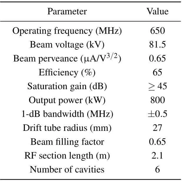
Table 1. Main design parameters.
3. Beam–wave interaction simulation
The RF section plays an important role in efficiency,gain and bandwidth, which includes 6 cavities and drift tubes between cavities. The drift length and the cavity characteristic parameters such as frequencies, characteristic impedance,coupling coefficients and external quality factorQeof input and output cavity are optimized to obtain maximal efficiency in the absence of returning electrons in the output cavity.At the same time, the length of klystron should be as short as possible. With the development of computer technology,many codes for the klystron simulation have been developed,which makes computer simulation technique to become a main method for klystron design. Several different codes are used to simulate the beam–wave interaction. AJDISK[13]is a onedimensional (1D) large signal klystron simulation software based on disk model developed by SLAC, which is mainly used for parameters optimization due to its fast calculation speed. The klystron efficiency depends largely on the quality of electron bunching. The high fundamental beam current and the low velocity spread are prerequisites for obtaining the high efficiency. The simulation results using AJDISK are shown in Fig. 1. The maximum ratio of fundamental current to DC current is 1.77. The minimum ratio of electron velocity to light velocity after the deceleration of the output cavity is 0.04, which can prevent the klystron oscillation caused by reflux electron. The total length of RF section is 2.1 m.
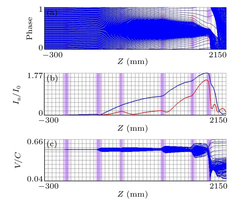
Fig.1. AJDISK simulation results. (a)Phase plot,(b)current plot,(c)velocity plot.
KLYC1D/1.5D is a free klystron simulation code developed by Jinchi Cai and Igor Syratchev,[14]at European Organization for Nuclear Research(CERN).KLYC1.5D based on the ring model uses two-dimensional(2D)cavity field but the particle motion is one-dimensional. In our simulation,the 2D electric field is imported from CST and the layer number is set to be 8. Due to the inhomogeneous cavity field,the transverse depression of potential and the variation of the space charge force over the beam cross section, the beam stratification occurs, as shown in Fig. 2. The fundamental current increases gradually along the radial direction,which results in the drop of klystron efficiency by 4.5% compared to the 1D and 1.5D simulation results in KLYC code.
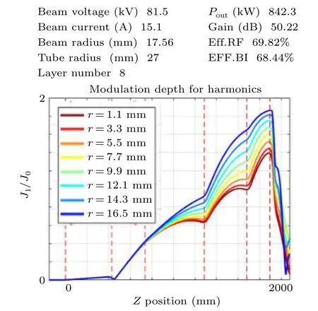
Fig.2. KLYC1.5D simulation results.
EMSYS[15]is a 2.5D klystron simulation software based on PIC algorithm,which is used to optimize the focusing magnetic field to get maximum efficiency and prevent beam interception. To adjust the magnetic field conveniently,the electromagnet focusing system is adopted,which consists of 15 coils and one bucking coil. These coils are divided into three region such as electron gun region,bunching region and output region to reduce the number of focusing coil power supply.After beam optics design, the optimization of magnetic field is mainly focused on the output region. The magnetic field increases from 180 Gs(1 Gs=10−4T)to 270 Gs to compensate the growth of the space charge force along the longitudinal direction,as shown in Fig.3.

Fig.3. EMSYS simulation results. (a)Beam profile plot,(b)energy profile plot,(c)magnetic field profile plot.
The PIC solver of CST[16]is a 3D self-consistent beam–wave interaction simulation code,which can completely simulate the real structure of klystron with high accuracy. Therefore,to study the effect of field asymmetry caused by coupler of input and output cavities on klystron efficiency, a full 3D simulation of klystron has been carried out in CST,as shown in Fig.4. The particle interface is defined to import particle data from a gun simulation used tracking solver in CST.The magnetic field is imported from 3D solenoid design. The asymmetry gap field of the output cavity due to the perturbation of the coaxial coupling loop results in efficiency degradation of 4.5%.
The simulation results with different codes are summarized in Table 2.
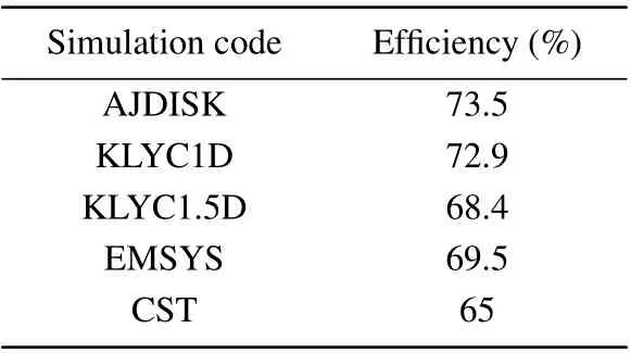
Table 2. Efficiency with different codes.
In the manufacturing process, the cavity frequency error occurred sometimes. The effect of cavity frequency error on efficiency of klystron is simulated in EMSYS, as shown in Fig.5. Because the frequency of the second cavity is close to operating frequency and the unloaded quality factorQis high,the cavity impedance is sensitive to the variation of frequency,which results in a big change in the klystron gain. However,the efficiency can maintain almost the same value by adjusting the input power. Therefore,the frequency tolerance of all cavities is allowed to be±0.5 MHz.
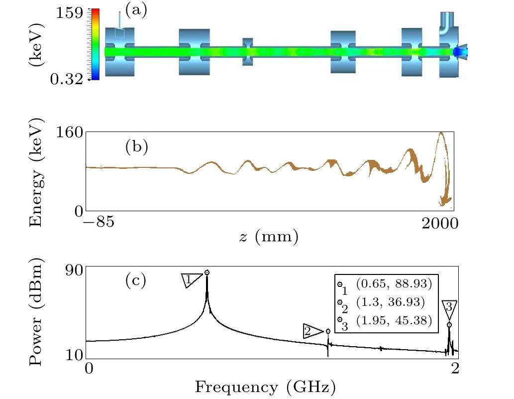
Fig.4. CST simulation results. (a)Beam profile plot,(b)energy profile plot,(c)spectrum plot.

Fig.5. Efficiency as a function of frequency error.
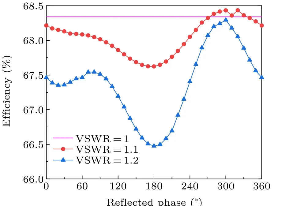
Fig.6. Efficiency as a function of reflected phase at different VSWRs.
The mismatch load can affect the efficiency of klystron due to the variation of gap impedance of the output cavity,[17]which is also simulated in KLYC1.5 code to keep a safety margin for stable operation even at voltage standing wave ratio(VSWR) of 1.2 without returning electrons from the output gap. Figure 6 shows that the maximum efficiency degradation is less than 2%with the variation of reflected phase in the case of VSWR of 1.2.
4. Cavity design and cold test
The klystron includes six cylindrical reentrant cavities with knife edge nose operating in the TM010mode. The third cavity is a second harmonic cavity. The main cavity characteristic parameters determined by beam–wave interaction simulation are listed in Table 3.
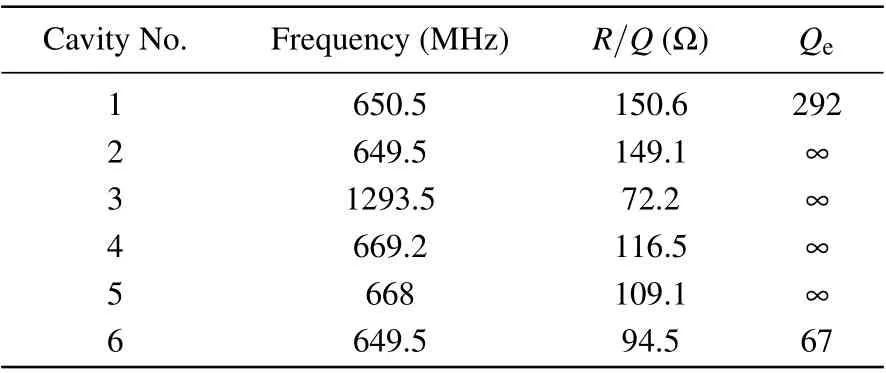
Table 3. Cavity parameters.
While designing the cavities, we pay attention to several issues such as high order mode oscillation,electric field breakdown, multipacting effect and ohmic heat loss. The high order mode oscillation like TM011can be suppressed by keeping mode frequency away from the beam current harmonic frequency.[18]The electric field breakdown usually occurs in the nose cone of the output cavity. The electric field distribution of the output cavities is shown in Fig. 7. The maximum surface electric field is 14.2 MV/m, which is less than 23.6 MV/m calculated from Kilpatrick criterion.[19]The coupling loop of the output cavity is designed to achieve externalQof 67.

Fig.7. Electric field distribution of the output cavity.
The multipacting effect can be avoided by manufacturing grooves in nose cone.[20]The oxygen free high conductivity copper(OFHC)is used for cavity fabrication due to the low ohmic losses and the high thermal conductivity. All cavities are cooled by water to take away the ohmic heat loss on the copper surface and maintain the cavity frequency stable.The gap distance and the drift tube radius are determined in beam–wave interaction simulation. With the aid of electromagnetic simulation code CST,the length and diameter of all cavities have been optimized to meet cavity characteristic parameters requirements. To avoid electron bombardment on the end drift tube of the output cavity, the asymmetric nose cone gap and enlargement of the end drift tube radius are adopted. All cavities were fabricated at Institute of Electronics. After several iteration of cavity radius adjustment during the manufacturing process,the cavity frequency was achieved the desired value before final brazing. After manufacturing,all cavities are measured with Keysight vector network analyzer. The probe method is used to measure the frequency and unloadedQof the intermediate cavities. The externalQof the output cavity are measured accurately with group delay time method.[21]And the frequency at the maximal group delay time is the cavity resonant frequency. Figure 8 shows the cold test of the output cavity. The resonant frequency and externalQare 649.5 MHz and 69 respectively,which are in good agreement with the simulation.
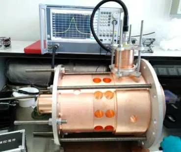
Fig.8. Cold test of the output cavity.
5. Conditioning and high-power test
A high-power test bench for the first prototype klystron was built, which mainly includes a pulse step modulation(PSM)power supply,an RF driver amplifier,a ferrite dummy load, WR1500 waveguide transmission system, RF power measurement system,interlock system and water-cooling system. Figure 9 shows the first prototype klystron test bench.
The commissioning of the high-power klystron is carried out at first,which includes gun high voltage conditioning,high voltage beam conditioning and RF power conditioning. Then,the pulse RF power test was performed using a 400-kW ferrite dummy load. A waveguide directional coupler with 60-dB coupling factor and 27-dB directivity is used for the measurement of klystron forward and reflected power. When the gun operated at DC voltage of 80 kV and current of 15.4 A, the klystron peak power reached 804 kW at 40%duty cycle. The pulse width and repetition frequency are 8 ms and 50 Hz respectively. The output efficiency is 65.3%. Also, the output power was verified from inlet and outlet temperature difference and flow rate of the cooling water for the dummy load,which is about 3% lower than directional coupler test result mainly due to the insertion loss of the waveguide transmission system from the klystron to the dummy load. No instability,such as multipactor,spurious frequency or sideband frequency due to returning electron is observed.The transfer curve shows the saturation power achieved at input power of about 16 W in Fig.10. Figure 11 indicates that the 1-dB bandwidth is about±0.8 MHz and the gain is about 47 dB. Figure 12 compares the relation between output power and beam voltage in EMSYS code with the test results. After the 800-kW dummy load delivered to IHEP,the CW RF power test was started. The ceramic of the coaxial window was cracked when the CW power is achieved about 700 kW.No punctures and surface discharge phenomena are found on the air side of the ceramic. The reason for the failure of coaxial window need to be analyzed in detail after the klystron was disassembled.
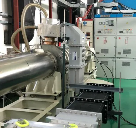
Fig.9. Klystron high-power test bench.
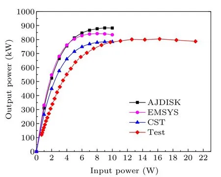
Fig.10. Klystron transfer curve.
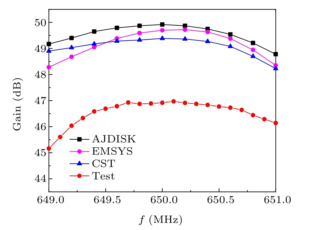
Fig.11. Klystron bandwidth.
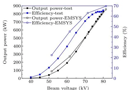
Fig.12. Relation between output power and beam voltage.
6. Conclusion
The R & D of 800-kW CW klystron operating at 650 MHz for CEPC was started in 2016. So far,the first prototype klystron has been designed,fabricated and high-power tested. We succeeded in obtaining 804-kW peak power in pulse mode and about 700-kW average power in CW mode.The high-power test results are in good agreement with simulation. During the whole process, we have accumulated a lot of design and fabrication experience for high power CW UHF klystron. The design and manufacturing of next prototype of high efficiency klystron in the second phase are in progress.
Acknowledgments
We would like to acknowledge the Institute of Electronics(IE)and Kunshan GuoLi Electronic Technology Company(GLVAC) for their great cooperation. Thank are also due to colleague in accelerator group at IHEP for their valuable contributions.Project supported by Yifang Wang’s Science Studio of the Ten Thousand Talents Project.
猜你喜欢
杂志排行

Chinese Physics B的其它文章
- Magnetic properties of oxides and silicon single crystals
- Non-universal Fermi polaron in quasi two-dimensional quantum gases
- Purification in entanglement distribution with deep quantum neural network
- New insight into the mechanism of DNA polymerase I revealed by single-molecule FRET studies of Klenow fragment
- A 4×4 metal-semiconductor-metal rectangular deep-ultraviolet detector array of Ga2O3 photoconductor with high photo response
- Wake-up effect in Hf0.4Zr0.6O2 ferroelectric thin-film capacitors under a cycling electric field