Design and evaluation of prototype readout electronics for nuclide detector in Very Large Area Space Telescope
2022-07-26HaiBoYangXianQinLiYuHongYuYongChenJieKongYongJieZhangShuWenTangJianHuaGuoBingYangFengJiaoSuWenJianSunJinXiangWangChengXinZhao
Hai-Bo Yang· Xian-Qin Li · Yu-Hong Yu · Yong Chen · Jie Kong·Yong-Jie Zhang · Shu-Wen Tang· Jian-Hua Guo· Bing Yang ·Feng-Jiao Su · Wen-Jian Sun · Jin-Xiang Wang · Cheng-Xin Zhao
Abstract China plans to develop the next generation dark matter particle explorer satellite, referred to as the Very Large Area Space Telescope (VLAST). As an essential step in this process, the prototype design of detectors and electronics for the VLAST is currently underway. The nuclide detector is a core detector in the VLAST.It mainly measures nuclides’ charges and distinguishes high-energy gamma rays and electrons. This paper will discuss the prototype readout electronics for the VLAST’s nuclide detector, which accurately measures the charge signal of the photomultiplier tubes using the VATA160 applicationspecific integrated circuit chip; furthermore, we consider a series of critical problems, including radiation-hardening and environment monitoring.The test results show that the system exhibits stable operation, good performance, and good technical indicators. Furthermore, each electronic channel achieves a dynamic range of 0–12.5 pC, the random noise level exceeds 1.6 fC, and the integral nonlinearity exceeds 0.35%.
Keywords Dark matter · VLAST · Nuclide detector ·Prototype readout electronics·VATA160·Large dynamic range · Irradiation test · Performance test
1 Introduction
China’s first astronomical science satellite, the DArk Matter Particle Explorer (DAMPE) ‘‘Wukong,’’ was successfully placed into the predicted sun synchronization orbit using the Long March 2D carrier rocket, launched from the Jiuquan Satellite Launch Center on December 17,2015. It has been stably operated for more than six years,retrieving a large amount of data [1, 2]. Physicists have published several observation results, including direct measurements of high-energy cosmic-ray electrons and positrons in the energy range 25 GeV–4.6 TeV [3], measurements of cosmic ray proton fluxes with kinetic energies from 40 GeV to 100 TeV [4], and measurements of the energy spectrum for cosmic ray helium nuclei from 70 GeV to 80 TeV [5]. However, this is not sufficient to determine whether dark matter exists. To strengthen our ability to search for dark matter particles via gamma rays and cosmic ray sources, China plans to develop the Very Large Area Space Telescope(VLAST) [6].The VLAST is a new generation of cosmic ray detector with a higher expected performance;it will measure high-energy gamma rays and electrons of up to 20 TeV and further expand the range of nuclides charges.It is expected that several of the existing suspect signals will be eliminated or confirmed,and the search for dark matter will continue. Figure 1a shows the detector profile of the VLAST(from the current proposal). The core detectors are the calorimeter (ECAL),nuclide detector (ND), anti-coincidence detector (ACC),silicon tracker (STK), neutron detector, and so on. The ECAL measures the total energy of incident cosmic rays.The ND identifies cosmic ray nuclides and distinguishes between high-energy electrons and gamma rays. The ACC is used to distinguish neutral particles from anti-coincidence charged particles.The STK measures the direction of incident cosmic rays and has already been researched[7, 8]. Finally, the neutron detector further improves our ability to distinguish electrons and hadrons, by measuring secondary neutrons.
The nuclide detector will apply an extended version of the plastic scintillator detector (PSD) used in the DAMPE[9, 10]. It consists of multiple plastic scintillator strips,with a total size of approximately 2 m × 2 m. The electronic signal is read out from both ends of each plastic scintillator strip. The nuclide detector needs to cope with an event rate of ~2–4 kHz. In contrast, the event rate of the PSD in the DAMPE is 50 Hz, and its size is 0.82 m × 0.82 m. The event rate and size of the nuclide detector are 80 and 6 times higher than those of the DAMPE PSD, respectively. In addition, the nuclide detector participates in system triggering, which can improve its discrimination of particle events. Thus, the nuclide detector can better identify nuclides in cosmic rays.
This nuclide detector distinguishes charged particles and photons and identifies heavy-ion particles in the range of Z = 1–40. Hence, the readout electronics should have an extensive dynamic range,to enable them to read weak and strong signals. Therefore, the light yield of the plastic scintillator strips is tuned to its maximal limit. The photomultiplier tubes(PMTs)are designed in a double dynode readout scheme: both the charge signal of the first stage dynode and the charge signal after the first and second stage dynodes are read out.The first stage dynode(with the highest gain) corresponds to the low-energy range, whilst the second stage dynode(with the lowest gain)corresponds to the high-energy range.The two output signals are sent to different channels of the readout electronics. Every end of the PSD crystal corresponds to a PMT with two readout channels; these need to reach a total dynamic range of 2.5 × 10⁵[0.1–2500 million instructions per second(MIPs)]. In total, 160 PMTs are required, and the corresponding number of readout electronics channels is 320.To allow each plastic scintillator strip to cover the dynamic energy range of 0.1–2500 MIPs, the readout electronics channels must achieve a minimum charge measurement sensitivity of 24 fC. In this paper, the development of the prototype readout electronics (PREs) for the nuclide detector is described. The research results will provide possible solutions for the engineering design of the VLAST.
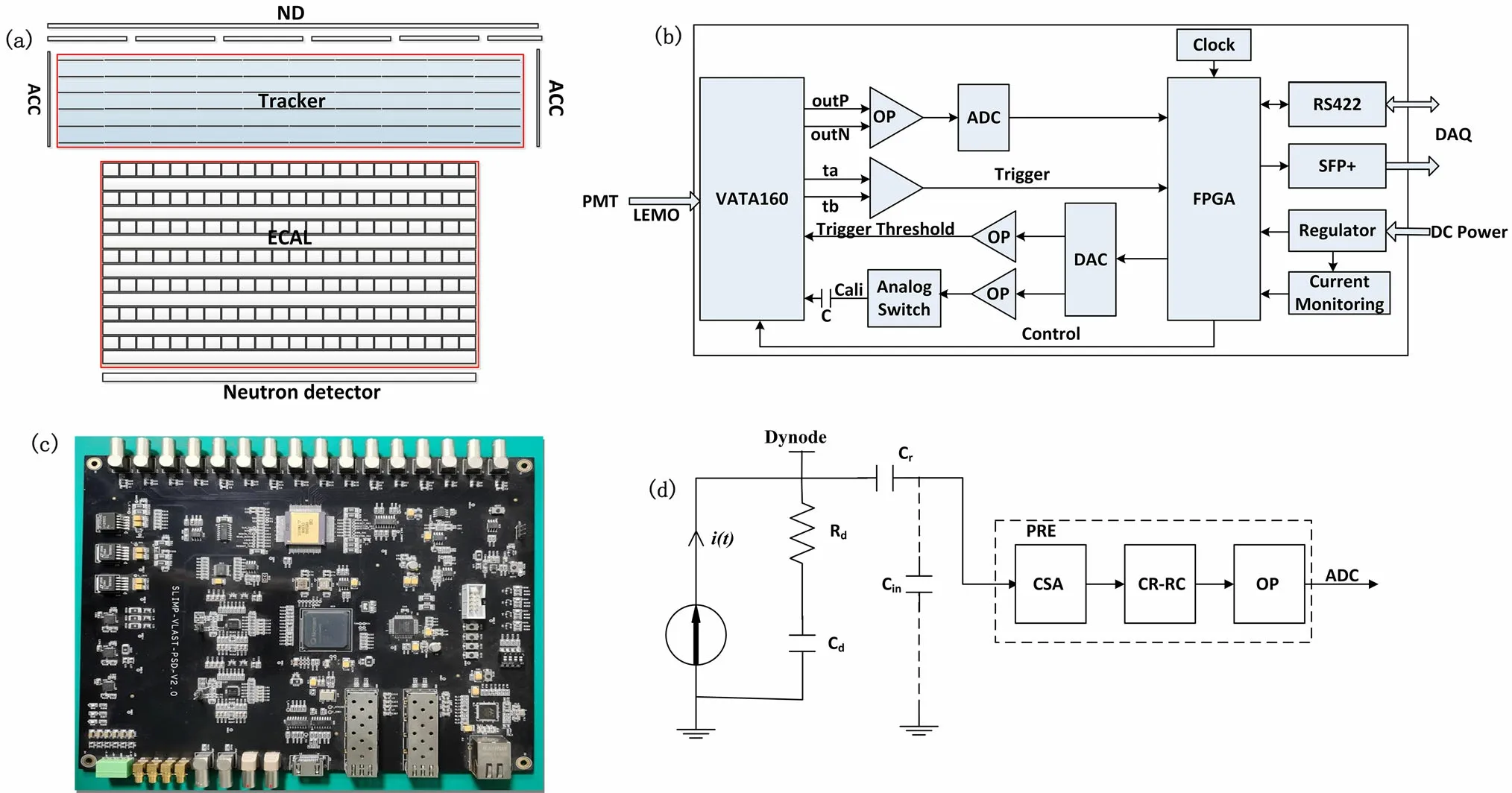
Fig. 1 (Color online) a Architecture of the VLAST payloads. b Block diagram of the prototype readout electronics. c Image of the prototype readout electronics. d Front-end equivalent circuit
2 Readout electronics
Solar panels are used to power the satellite platform;hence, the total power consumption of satellite loads is strictly limited, and low-power electronic components should therefore be used. Generally, each readout electronics power consumption is less than 2 W. In addition,the readout electronics must be able to endure harsh space irradiation. With the energy requirements for cosmic ray detection and the limitations of satellite power consumption and hardware, the PRE must have high speed, low power consumption, low noise, and radiation-tolerant characteristics. The PRE uses the commercial applicationspecific integrated circuit (ASIC) chip VATA160 (developed by IDEA) to realize low-noise and large-dynamicrange charge measurements. The complete front-end readout electronics prototype is designed to use the VATA160 as the core chip.For convenience of testing,the LEMO standard connector was selected as the signal input connector.Owing to the space limitations of this connector,the PRE was only designed with 16 signal input channels.Figure 1b,c show an overview and picture of the PRE.The PRE includes the VATA160 circuit, instrumentation amplifier circuit, analog-to-digital conversion circuit, calibration circuit, current monitoring circuit, field-programmable gate array(FPGA),power management circuit,and communication interface circuit.First,the PMT output charge pulse is sent to the input of the VATA160 via the LEMO coaxial cable. Next, the signal undergoes chargesensitive preamplification as well as shaping and peak holding inside the VATA160; finally, a proportional differential current is outputted.The instrumentation amplifier circuit completes the current-to-voltage and differentialsignal-to-single-ended-signal conversions. The analogueto-digital converter (ADC) digitizes the output of the instrumentation amplifier circuit with a sampling frequency of 2.5 MHz. The FPGA receives the digitized results,packs the data, and finally sends it to the data acquisition(DAQ) module via the data transmission interface. In addition,the PRE can receive serial data commands via the DAQ module through the communication interface, whilst the PRE replies to response commands or status parameters. An optical link and RS422 interface are used for communication between the PRE and DAQ. In addition, a current sampling circuit is used on the PRE to perform online monitoring of the current.Moreover,the PRE can be calibrated online, which is convenient for the monitoring system’s long-term stability.
Figure 1d shows the PRE’s transfer function, Cinis the equivalent input capacitance of the VATA160.Cris a readout capacitor placed in series with the dynode; it has a capacitance of 0.5 nF in the current design,and it also plays a role in high voltage isolation. Rdis used to supply high voltage to the anode with a resistance of 10 KΩ.Finally,Cdis a high voltage bypass capacitor on the divider of PMT,with a capacitance of 1 nF. The equivalent input capacitance is

2.1 VATA160 ASIC

Fig. 2 a Block diagram of the VATA160. b Block diagram of the overvoltage protection circuit. c Block diagram of the instrumentation amplifier circuit
The VATA160 ASIC chip[11,12]measures the charge collected by the plastic scintillator strips and generates triggers. Each VATA160 has 32 input channels, which meets the design requirements of multi-channel, high integration, and low power consumption. Figure 2a shows a block diagram of the VATA160. Each signal channel consists of a charge-sensitive pre-amplifier connected to a slow shaper with a nominal 1.8–2 μs shaping time and a fast shaper with a 100 ns shaping time. The charge-sensitive preamplifiers are optimized for positive input charge and provide a dynamic input range from 0 to + 13 pC.The slow shaper is used for energy measurement. The energy signal from each slow shaper is stored in the Sample and Hold block. The energy signal from all channels is transmitted through one differential analog current output buffer(AOB), which is controlled by a multiplexer. Thus, an external ADC is necessary to digitize the differential signal from the AOB. The fast shaper is used for trigger generation. Each fast shaper output is connected to a comparator and triggers when the pulse height exceeds the standard threshold (Vthr) level. All the comparators’ outputs are summed by a logic OR module to generate a trigger output.The chip requires positive and negative supply voltages (–2.5, + 2.5 V). The total power dissipation of the chip is 185 mW in steady state and has a 225 mW maximum,depending on the readout rate. The chip has a 165-bit configuration register that allows us to program various features of the chip, including the triggering component,programmable gain stage,trim digital to analog converters(DACs), test mode, and channel disabling. The VATA160 allows us to test and measure its gain by injecting an external charge. It has a bias generation network that generates all bias currents and voltages needed for its operation.The VATA160 is also radiation tolerant[13,14].
2.2 Protection circuit
A sudden change in the PMT’s high voltage or an electrostatic discharge on the readout electronics will lead to a high transient voltage coupling to the input of the VATA160 chip. This may damage the chip or reduce its lifetime. Hence, an overvoltage protection circuit at the signal input of the PRE is compulsory. As shown in Fig. 2b,the clamping diode can be quickly turned on when the input signal voltage exceeds–0.8 V or falls lower than–3.2 V. The 1N4148 fast-switching diode was selected for this.This overvoltage protection circuit has been verified in the laboratory.A large voltage pulse from the signal source is injected into the VATA160 through a capacitor. The current of this VATA160 chip increases abnormally,which poses a risk of chip damage. After adding this overvoltage protection circuit, the abnormal current of the VATA160 chip no longer arose. Hence, this circuit can effectively protect the VATA160 chip from damage under large transient current changes.
2.3 Analog-to-digital converter circuit
The output of the VATA160 chip is a differential current signal. Before the analog-to-digital conversion, the output of the VATA160 must be preprocessed. The differential current signal should be converted to a single-ended voltage signal.Next,the voltage signal is adjusted to a dynamic range of 0–5 V via an instrumentation amplifier circuit.The instrumentation amplifier circuit is composed of operational amplifiers, as shown in Fig. 2c. To effectively suppress the common mode noise,the upper and lower bypath parameters of the amplifying circuit must possess good symmetry. In the design, the same operational amplifier package is selected for the two operational amplifiers in the first stage of the circuit; hence, both process parameters can be kept consistent.The AD9243 of the analog devices facilitates digitization of the signal.The AD9243 is a 14-bit ADC. The input analog voltage signal ranges from zero to 5 V.The power supply voltages of the AVDD and DVDD are + 5 V, and the power supply voltage of DRVDD is + 3.3 V.
2.4 FPGA circuit
Under the control of the main FPGA, each PRE is responsible for receiving the charge signal from the detector and packaging the data to be uploaded to the DAQ system. The FPGA logic unit primarily consists of the VATA160 driver,data transmission,and command control modules. Therefore, the FPGA is a critical component of the PRE. The Flash-based SmartFusion2 (SF2) FPGA(M2S090T-1FGG484I [15]) from Microsemi was chosen as the main FPGA.Compared with the configuration unit in the SRAM-based FPGA (which is easy to flip), the Flashbased FPGA has a floating gate structure which is not very sensitive to single event effects and is less susceptible to radiation. Therefore, this FPGA is suitable for radiationhardened applications and has several radiation-hardened functionalities [16, 17].
2.5 Current-monitoring circuit
Single event latch-up(SEL)may lead to a large transient current and damage the electronic component during PRE operation. Thus, the power supply of the PRE needs to be switched off when SEL occurs. As shown in Fig. 3a, a current monitoring circuit was implemented in the PRE. It consists of a multi-channel 200 Kbps ADC, operational amplifiers, and sampling resistors. The TLK2548 from Texas Instruments was used as the ADC.The PRE current is sampled every second.If three successive sample current values exceed the pre-set threshold value, the PRE will automatically power off to protect itself. Afterwards, the PRE is powered on after 10 ms to prevent the electronic components from being burned by the large transient current arising from the SEL.
2.6 VATA160 calibration and threshold generation circuit
The calibration module is mainly used for system performance calibration and trigger threshold generation. As shown in Fig. 3b, the calibration circuit primarily consists of a DAC, two operational amplifiers, and an analog switch.The TLV5638 from Texas Instruments was used as the DAC. This DAC has two output channels: one calibrates the signal channels in the VATA160 ASIC;the other generates the trigger threshold. To calibrate the VATA160 ASIC, the DAC generates a voltage signal of equal step length; this is sent to the analog switch after the op-amp follows the voltage. A step pulse can then be generated when the analog switch is turned on.The amplitude of this voltage pulse ranges from zero to Vcaj. Using an onboard 10pF ceramic capacitor,this voltage pulse is converted into a charge pulse and sent to the VATA160’s input pin for calibration.By selecting the input channels,all channels of the VATA160 ASIC are calibrated stepwise. The linearity and noise of all signal channels are measured by plotting the scanned curves. To set the trigger generation threshold for the VATA160, the DAC generates a voltage signal.This voltage signal feeds into an adder and subtractor circuit, to create the trigger threshold voltage into the VATA160’s corresponding input pin. The trigger generation scheme has been presented in Sect. 2.1. The trigger signal from the VATA160 is a differential current output signal (ta and tb), which is converted into a voltage signal by a 1 KΩ resistor at each end of the differential current signal outside the VATA160. The DS26LV32, a highspeed complementary metal–oxide–semiconductor(CMOS) differential receiver, converts the differentialtrigger signal into a single-ended voltage signal and sends it to the main FPGA.

Fig. 3 a Block diagram of current monitoring circuit.b Block diagram of the VATA160 calibration and threshold generation circuit
2.7 Power supply circuit
A highly reliable power supply scheme was designed for the PRE, to ensure its stability. The PRE requires three power supplies (+ 6 V, + 3.3 V, - 3.3 V), provided by an external power source. A set of power regulators generate the voltage to the main FPGA, VATA160, and the other onboard components. Firstly, the PRE’s three input power supplies are designed with high stability, according to the specifications. Secondly, the power supplies for the FPGA, VATA160, ADC, OP, and DAC are converted by low dropout regulators from the three input power supplies.These designs ensure stability in the PRE.
3 Performance measurement
To evaluate the function and performance of the readout electronics, we conducted a series of tests.
3.1 ADC dynamic performance
An effective number of bits(ENOB)test was performed using the specifications defined in IEEE 1057-2017 [18].For an input sine wave signal with a specified frequency and amplitude, the ENOB is defined as

where N is the number of bits digitized, FSR is the fullscale range of the recorder,NAD is the noise and distortion,and εQis the root mean square (RMS) ideal quantization error.
In the test, a sine wave signal was generated with a peak-peak value of ~2 V, the frequency was 4 kHz.Figure 4a gives the typical results, NAD = 0.45 mV,

. These values are substituted into Eq. (6) to obtain ENOB = 14 - log2(0.45/0.0882) = 14 - 2.35 = 11.65 bits.
3.2 Baseline characterization
The baseline characterization aims to determine the baseline noise of each channel in the readout electronics system. The test results are shown in Fig. 4b, which indicates the RMS values for each channel.The horizontal axis denotes the numbers of the 16 input channels, and the vertical axis shows the channel value of the ADC.The PRE was placed in a shielding box with unconnected signal input pins. As shown in Fig. 4b, the RMS of all channel baselines was less than the two ADC values, equivalent to 1.6 fC; this represents a relatively small (0.013%) proportion of the readout electronics’ dynamic range.
3.3 Channel linearity test
3.3.1 Signal source test
In the test, a precise signal source (Tektronix AFG3252C[19])was used to scan and test each channel of the PRE, to understand the performance of each readout electronics channel. During the test, the signal source was used to output a voltage pulse signal. The voltage pulse signal was sent to a series capacitor. After the capacitor, a charge pulse was generated and sent to each input channel of the PRE. When the series capacitor was 10 pF and the signal source generated a 1 V voltage signal, the input charge was Q = C × U = 10 pF × 1 V = 10 pC. For the test, the signal source had to generate voltage signals of different amplitudes (50 mV–1.5 V) with a step length of 50 mV, and each amplitude was tested 1024 times. Figure 4c is the linear fitting curve for one of the channels,where the horizontal coordinate is the input charge in fC and the vertical coordinate is the output ADC channel value. The linear fitting function of the signal source test was ‘‘y = 11.67 x + 349.63’’. The fitting result was obtained by fitting the 0–12.5 pC interval in the linear region. It can be found that the integral nonlinearity of the channel exceeded 0.35%.
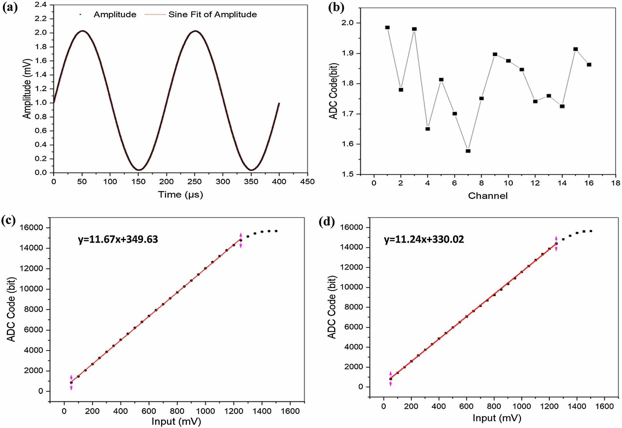
Fig. 4 a Reconstruction of 4 kHz sine wave signal sampled at 2.5 MHz. b RMS test results of all channels on the PRE. c Channel scan test linearity results of the prototype readout electronics. d Calibration test linearity results of the prototype readout electronics
3.3.2 Calibration test
The calibration test can verify the effects of the operating performance parameters for each signal channel upon the readout electronics. The calibration circuit generates a voltage pulse signal with different amplitudes and equal steps. The voltage pulse signal is sent to the VATA160’s calibration signal input pin via the 10 pF capacitor. All signal channels were scanned and tested. Figure 4d shows the linear fit curve for one of these channels.The horizontal coordinate is the input charge in fC.The vertical coordinate is the output ADC channel value.The linear fitting function of the calibration test was ‘‘y = 11.24 x + 330.02’’. By applying a linear fit, the linear region ran from 0 to 12.5 pC, and the non-linearity was less than 0.3%.
Under an identical input voltage, the ADC code of the calibration test was lower than the signal source test. This is because the voltage output of the calibration circuit passes through paths involving analog switches and resistors;this produces some amplitude attenuation but does not affect the system calibration. In addition, the non-linearity of the calibration test is slightly less significant than that of the signal source test.This is because the calibration circuit is located on the PRE, which is closer to the charge measurement channel. The noise and interference of the calibration signal were insignificant.
3.4 Equivalent noise level test under different input signals
To more precisely identify the variation of the equivalent noise under different input signals,scanning tests were performed using the signal source and onboard calibration circuit, respectively. The signal source and onboard calibration circuit generated voltage signals from zero to 1500 mV, respectively, in steps of 50 mV. The test was performed 10,000 times for each voltage amplitude, to obtain a random distribution of test results under the given input signal amplitude. The RMS value was considered to be the equivalent noise level of the board. Figure 5a is the test result obtained when using the signal source and onboard calibration circuit to test a certain channel of the PRE. The horizontal coordinate is the input charge in fC;the vertical coordinate is the RMS percentage compared to the measured average value. It is found that the random error tends to decrease roughly under the increase in the input signal amplitude. Figure 5a suggests that the equivalent noise level of the onboard calibration circuit is significantly higher than the test results of the signal source.This is because the calibration circuit is located directly on the PRE,and the voltage signal used for calibration suffers less interference.
3.5 Temperature stability test
The PRE was placed inside a temperature chamber,and the other modules were placed in the external environment.The change of the baseline with respect to temperature in the PRE was measured. In Fig. 5b, the horizontal coordinates denote temperature values in degrees Celsius,and the vertical coordinates are the baseline values for each channel. Figure 5b shows the variation of the baseline for Channels 4,10,12,and 16 with respect to temperature.The baseline value increased slightly under the temperature increase. However, the baseline variation across different channels of the VATA160 was stronger.The baseline drift mainly arises from the change in the characteristics of the VATA160 chip itself. In the offline data analysis, the baseline drift of the PRE was corrected by deducting the baseline value in real-time.
3.6 Channel-to-channel crosstalk test
The channel-to-channel crosstalk tests were performed on Channel (CH) 7 using a signal source. The test method proceeded as follows:the charge scanning test of CH7 was conducted using the signal source. Due to crosstalk, the measured values of these adjacent channels also changed with respect to the input value of CH7. The different channels can be plotted by taking the input charge of CH7 as X and the ADC measurement results of other channels as Y to draw a curve. The linear fitting of these curves was performed,and the coefficient of the slopes was defined as the crosstalk coefficient value. Figure 5c shows the crosstalk coefficients to adjacent channels for standard signal(input charge: 0–15 pC). We found that the crosstalk coefficient of the adjacent channel was positive, at ~0.05%.The crosstalk coefficients of other nearby channels were negative, at approximately - 0.03%. In the PRE hardware design,the output signal of the high-gain channel produced by the PMT was connected to one VATA160 chip, and the output signal of the low-gain channel produced by the PMT was connected to another VATA160 chip, to minimize the crosstalk effect.
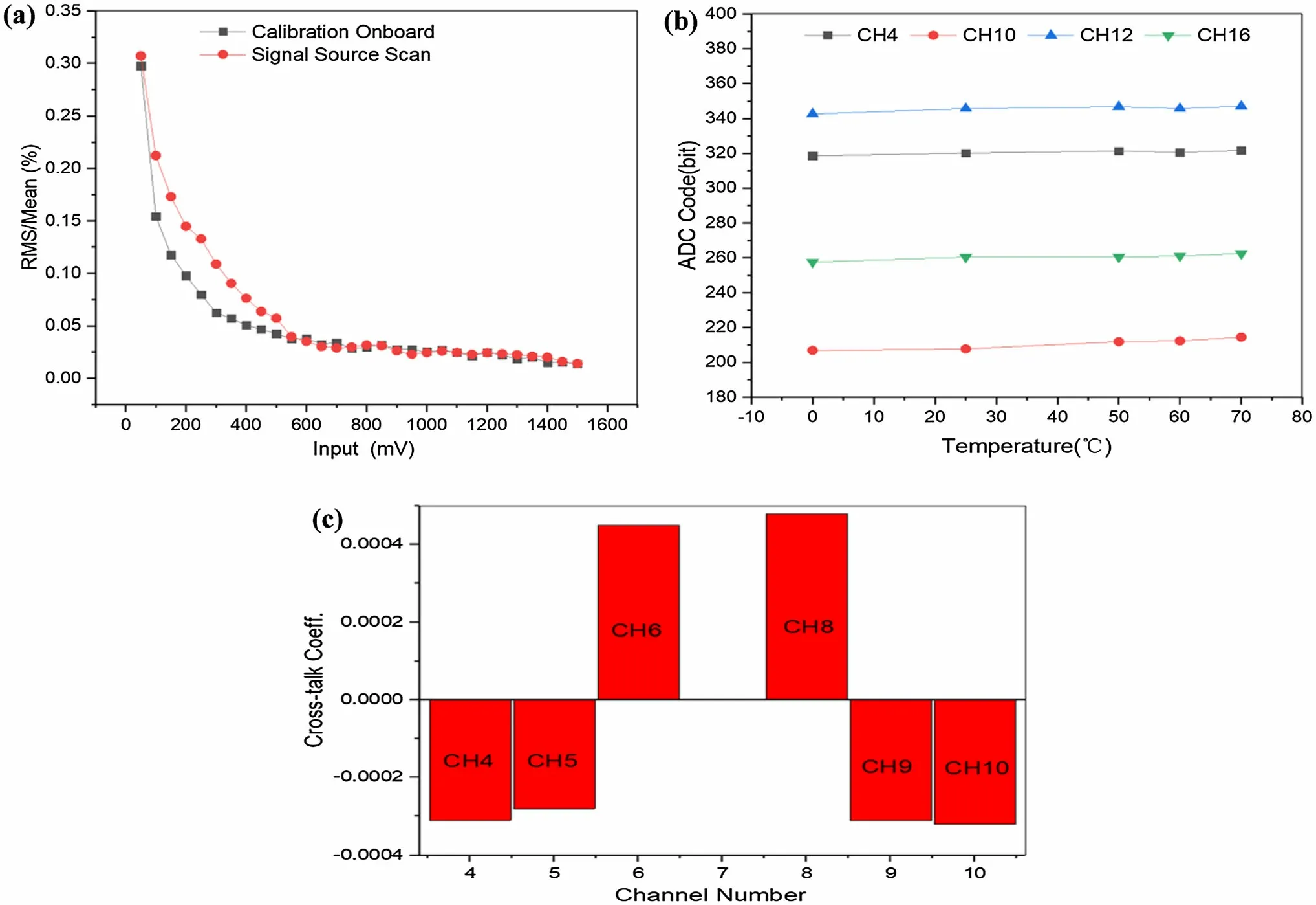
Fig.5 (Color online)a Results of relative error with respect to input charge.b Baselines of VATA160 Channels 4,10,12,16,which drift with respect to temperature. c Crosstalk coefficients (CH7 is the input channel)
3.7 Joint test with detector

Fig. 6 (Color online) a Joint test block diagram of the PRE and detector. b 90Sr radioactive source energy spectrum obtained from the test
To further verify the performance of the readout electronics system, it was necessary to combine the detector system with a joint test. Figure 6a shows the test block diagram of the readout electronic system and detector,which mainly consists of one detector, one high voltage power supply, one PRE, and one desktop computer. A radioactive source of90Sr [20] was used in the test. First,the particles emitted by the radioactive source were converted into a light signal via a plastic scintillator detector.Then,the light signal was converted into a charge signal by the PMT, and the readout electronics system processed the charge signal. Finally, the data were transferred to the desktop computer for processing.90Sr undergoes β-decay to release electrons and90Y,90Y will undergo further β-decay to generate stable90Zr; the maximum energy of the emitted β-decay is 2.274 MeV. The energy spectrum was continuous. The average energy of the energy spectrum was ~979.3 keV. The ratio of the maximum energy to the average energy was 2.32 [21, 22].Figure 6b shows the energy spectrum of the90Sr radiation source.The horizontal coordinate denotes the ADC values,and the vertical coordinate shows the counts for those values.The ratio between the maximum and average ADC values was ~2.3. This shows that the data obtained by our experiments are reliable. Through the above tests, the readout electronics design scheme was preliminarily confirmed to be feasible.
3.8 Irradiation test of the M2S090T-1FGG484I FPGA
An irradiation test was performed on this FPGA, to evaluate its radiation hardness. This was performed using the board in [23] at the back-streaming white neutron source of the China spallation neutron source (CSNS)[24,25].The energy coverage of neutrons emitted by white neutron sources ranges from several MeV to several hundred MeV. During the test, both single event upset (SEU)and SEL effects were monitored simultaneously. The FPGA was irradiated using a beam with a diameter of 30 mm during the experiment. Figure 7a, b show the test block diagram design and test setup of the irradiation test.The test system is mainly composed of a test board, a control board,and a PC.The optical fiber transmission link,Ethernet link,and basic units(e.g.,SRAM,PLL,Flip-Flop,etc.) were tested. All modules in the test design were completely separated to prevent failures in any one module from affecting the other modules.The PC was connected to the test board via three links: RS232, PHY, and JTAG.Together with the control board, the PC facilitates configuration and inspection of the operational status of the test board whilst generating log files and data sheets when recording the whole irradiation process. During the test period, when the system link function fails, the PC starts the power-on reset function in the monitoring system, to restart the test board.
SEL is potentially destructive and may cause permanent damage to electronic equipment. Therefore, an effective method is required to determine SEL in the test. SEL can cause sudden and significant increases in current consumption, leading to a noticeable non-linear current jump.The degree of change is strongly determined by the power supply voltage. Based on the above, the following method is implemented in the test system design, to identify SEL:First, we monitor the voltage and current of the power supply after turning it on and observing the current jump.If a current jump occurs and the amplitude is below 20 mA,the current is measured again after approximately one minute.Current jump disappearance should be produced by current consumption in the circuit instead of an SEL. On the contrary,if the current jump exceeds 20 mA,the power supply voltage is manually adjusted by 0.3 V to observe the current change. If an SEL phenomenon produces the current jump, the current will temporarily and irregularly return to the normal state after the voltage is adjusted.Otherwise, the potential current jump is caused by current consumption in the FPGA [26]. Suppose the SEL phenomenon occurs during the experiment; in that case, the corresponding control logic is required to record critical parameters (e.g., the operational status, occurrence time,and I–V parameters of the system)and restart the device in time.
The SRAM was performed by cyclically reading and writing the storage unit. According to the reading and writing results, the total number of errors in which the SRAMs were flipped by SEU was counted.To improve the precision and accuracy of the experiment, SRAMs should be instantiated in the design to the greatest possible extent.Moreover, to maximize the circuit utilization, the entire layout must be arranged in advance after synthesis. 72 L-SRAM (18 bit × 1024) and 2 U-SRAM (18 bit × 64)modules were used in the FPGA program. After initialization, the program writes 8’h0f to all SRAMs by default and enters the test mode. The controller judges the data read from the two sets of SRAMs. If the data error is detected, the controller calculates the bits of errors caused by unexpected flipping and writes the correct 8’h0f, to fix this error.Finally,all errors occurring within the test period are summarized.
The method to test the onboard PLL IP core is to cascade two PLLs for comparison. During the test, two scenarios were observed: one of the two PLLs lost the lock signal, and both the PLLs lost the lock signal simultaneously.This tests the PLL’s stability and verifies the impact of the PLL losing its lock upon the clock. If two PLLs always lose the lock signal,it indicates that the clock of the PLL is unreliable after losing the lock.This occurs because the frequency and phase of the clock are fixed after the clock is locked. Otherwise, the PLL can still output the clock, though the clock is in an unstable state at this time,and the impact on the sequential circuit is uncertain.

Fig. 7 (Color online) a Block diagram of the irradiation test. b Test setup of the irradiation test, taken from Ref. [27]. c Test results of the SRAM
In the optical fiber test, one board was put in the shielded area as a control board to realize data generation and inspection functions.The other FPGA board was a test board, which implements the loopback function in a radiation environment. The control board generates different types of binary numerical sequences and sends them to the test board at a speed of 2.5 Gbps. The test board in the radiation area receives serial data from the SFP interface.After deserialization, the original data are sent back to the parallel data end in a loopback mode. The control board can monitor the working status of SerDes, compare the difference between the data sent and received in real-time,count the number of errors of the two different channels and the number of link disconnections,and send the results to the PC for recording.
When testing the Ethernet link, the only main components exposed to radiation are the processor system and MAC core.Because the radiation exposure is limited to the SF2 FPGA chip, the performance of the off-chip physical layer PHY chip was not included in this radiation test.The test setup mainly consisted of the SF2 FPGA in the radiation area and a PC in the shielding area. These were connected and communicated via a network cable.The PC sent data packets to SF2 at a rate of 1000 Mbps. The data were received and looped in the SF2 FPGA. After receiving the data,the application layer immediately sent the data through the transmitting channel. Then, the PC compared the received and sent data,to test the working condition of the Ethernet link in the radiation.
In the test, the neutron fluence received by the SF2 FPGA was ~2.39 × 10⁹n/cm2. No destructive singleevent latch-up phenomenon occurred during the experiment.This shows that the FPGA chip can generally operate under the standard power supply voltage of 5 and 3.3 V.The PLL worked well; that is, the frequency and phase of the clock could be locked as usual,and the clock output of the PLL was meanwhile stable. Only one of the four flipflop chains (with an inverter) suffered an SEU in the test.The other three flip-flop chains all worked as intended.Several single-event errors occurred in the SRAMs. Figure 7c shows the number of errors with respect to time. In total, 23 SEUs occurred in the test. No problems were encountered with the FPGA optical fiber link.According to the calculated results, the cross-section of the SEUs was sufficiently low (greater than 1.02 × 10⁻⁸cm2). In addition,the cross-section of the SELs was also sufficiently low(greater than 4.3 × 10⁻¹⁰cm2). From the above experimental results, it can be seen that this Flash FPGA has a certain level of radiation hardness.
4 Conclusion
PREs (for pre-research of the nuclide detector subsystem in VLAST) were designed and tested. The PRE features 16 channels with a total power consumption of 1.6 W. The PRE primarily consisted of a charge measurement and threshold generation circuit, an instrumentation amplifier circuit, an ADC circuit, a calibration circuit, an environmental monitoring circuit, an FPGA circuit,a power management circuit,and a communication interface circuit.The readout electronics system was tested and found to work stably, achieve good performance, and exhibit good technical indicators. For example, each electronics channel achieved a dynamic range of 0–12.5 pC.Furthermore, the RMS obtained was less than 1.6 fC; the noise only accounted for 0.013% of the range of the entire readout system. Moreover, the integral nonlinearity of the channel exceeded 0.35%. To further verify the performance of the readout electronics system,we tested it with a90Sr radioactive source, to combine the detector system with a joint test. In addition, an irradiation test was performed on the FPGA to evaluate its radiation hardness.This shows that the FPGA has a strong anti-radiation capability. As a result, these prototype readout electronics can provide high integration, low power consumption, and a large dynamic range.
Author contributionsAll authors contributed to the study conception and design. Material preparation, data collection, and analysis were performed by Hai-Bo Yang, Xian-Qin Li, Yu-Hong Yu, Yong Chen, Jin-Xiang Wang, Jie Kong, Yong-Jie Zhang, Shu-Wen Tang,Jian-Hua Guo, Bing Yang, Feng-Jiao Su, Wen-Jian Sun, Jin-Xiang Wang, and Cheng-Xin Zhao. The first draft of the manuscript was written by Hai-Bo Yang, and all authors commented on versions of the manuscript. All authors have read and approved the final manuscript.
杂志排行

Nuclear Science and Techniques的其它文章
- Spatial resolution and image processing for pinhole camera-based X-ray fluorescence imaging: a simulation study
- Picosecond time-resolved X-ray ferromagnetic resonance measurements at Shanghai synchrotron radiation facility
- Nonrecursive residual Monte Carlo method for SN transport discretization error estimation
- Density fluctuations in intermediate-energy heavy-ion collisions
- Isospin effects on intermediate mass fragments at intermediate energy-heavy ion collisions
- Identification of anomalous fast bulk events in a p-type pointcontact germanium detector