Inorganic electron-transport materials in perovskite solar cells
2022-04-26LinXieLixiuZhangYongHuaandLimingDing
Lin Xie , Lixiu Zhang , Yong Hua , and Liming Ding
1Yunnan Key Laboratory for Micro/Nano Materials & Technology, School of Materials and Energy, Yunnan University, Kunming 650091, China
2Center for Excellence in Nanoscience (CAS), Key Laboratory of Nanosystem and Hierarchical Fabrication (CAS), National Center for Nanoscience and Technology, Beijing 100190, China
We have witnessed unprecedented progress of perovskite solar cells (PSCs) in last few years. The power conversion efficiency (PCE) has been boosted from 3.8% to the current record of 25.5%[1,2]. A typical PSC consists of a polycrystalline perovskite layer sandwiched between electron-transporting layers (ETLs) and hole-transporting layers (HTLs), with two configurations: regular (n–i–p) and inverted (p–i–n). Till now,the record efficiency of PSCs is still dominated by devices with the regular structure, which exploits inorganic electrontransport materials (ETMs) due to their low cost and chemical stability. This article overviews the latest progress of inorganic ETMs in regular PSCs, the interface treatments and other optimization strategies for high PCE and stability.
ETL plays a vital role in transporting and extracting photogenerated electrons and minimizing the charge recombination. The ideal ETMs in PSCs should possess following qualifications: a) solution processability; b) good energy level alignment with perovskite layer; c) high electron mobility; d) wide bandgap to ensure good transmittance in the visible light range; e) good chemical stability.
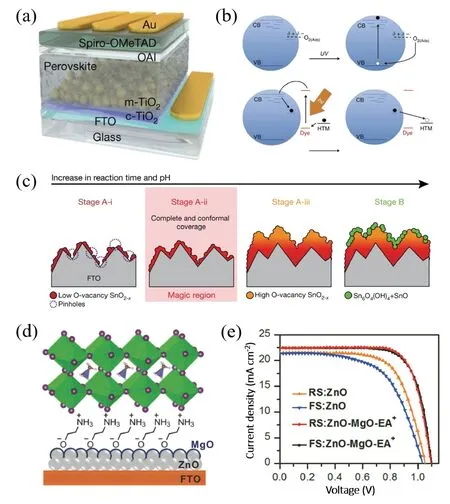
Numerous n-type inorganic semiconductors have been explored as ETLs in PSCs, such as TiO2[3,4], SnO2[5−7], ZnO[8,9],WO3[10,11], Zn2SnO4(ZSO)[12], BaSnO3(BSO)[13], etc. TiO2has been mostly used and many record efficiencies were obtained by using TiO2ETLs[3,4]. TiO2presents advantages like a wide bandgap to minimize parasitic absorption, an appropriate conduction band alignment with the perovskite for efficient electron injection, and good electron extraction capability. Currently, the most efficient structures adopt a compact TiO2layer via spray pyrolysis method and a mesoporous capping layer by spin-coating a TiO2paste diluted by ethanol/terpineol solvent (Fig. 1(a))[3,4]. The compact layer can protect perovskite layer from contacting the cathode and reduce leakage current, while the mesoporous layer can promote perovskite crystallization and facilitate charge transport.However, TiO2does have some disadvantages, e.g. UV instability (Fig. 1(b))[14], low electron mobility (0.1–4 cm2/(V·s))[15],and high processing temperatures (>450 °C)[3]. Though lowtemperature processing has been explored[16], the performance is not as good as that of high temperature-processed TiO2.
SnO2is a promising alternative in planar structure by virtue of higher electron mobility (240 cm2/(V·s))[15], suitable band structure, UV stability and low-temperature processibility. SnO2ETLs can be prepared via various approaches, including spin-coating nanoparticles[7], chemical bath deposition(CBD)[6], and atomic layer deposition (ALD)[17]. Spin coating SnO2nanoparticles diluted by H2O is easy to be processed,yielding many high efficiencies (>24%)[7]. But the open-circuit voltage (Voc) deficit is higher than that of TiO2. Given this,Seo et al. reported a facile carrier management through controlling the growth process of SnO2by using CBD[6]. By precisely controlling the reaction (Fig. 1(c)), a conformal film with sufficient coverage and ideal composition was achieved,leading to an enhanced carrier extraction and reduced nonradiative recombination, evidenced by high Voc(1.18 V) and PCE (certified 25.2%).

Fig. 1. (Color online) (a) Illustration of a regular PSC with ETL composed of compact TiO2 (c-TiO2) and mesoporous TiO2 (m-TiO2) layers. Reproduced with permission[3], Copyright 2021, Springer Nature. (b) The mechanism for UV instability of TiO2. Reproduced with permission[14], Copyright 2013, Springer Nature. (c) Illustration of synthesis progress of SnO2 ETL with stage A-i, A-ii, A-iii, and stage B through chemical bath deposition, with the increase of reaction time and pH. Reproduced with permission[6], Copyright 2021, Springer Nature. (d) Illustration of a planar n–i–p PSC with ZnO ETL modified by MgO and EA+. (e) J–V curves for PSCs with ZnO ETL with or without MgO-EA+ modification under forward and reverse scans. Reproduced with permission[8], Copyright 2018, John Wiley and Sons.
ZnO is another well-explored ETM[8,9]. Compared with TiO2, ZnO has similar matched energy level with perovskite and much higher electron mobility. ZnO with various nanostructures (e.g. nanorods, nanowires, nanoparticles,nanowalls, etc.) can be easily prepared at low temperature, enabling efficient electron extraction[18]. However, the problem of severe interface recombination and chemical instability greatly limits its application. The defects of ZnO induced during solution processing provide extra recombination path for charge carriers and degrade device performance. Besides, the alkaline surface of ZnO can trigger a deprotonation reaction with CH3NH3+(MA+), making the perovskite deposited on top susceptible to decomposition during thermal annealing[18].To solve this problem, element doping and interface modification were applied. Cao et al. modified ZnO surface by MgO and protonated ethanolamine (EA) to passivate the ZnO/perovskite interface and impede ZnO from reacting with perovskite, achieving hysteresis-free device with PCEs up to 21.1% (Figs. 1(d) and 1(e))[8]. ZnO is also an effective alternative for TiO2and SnO2in PSCs of MA-free perovskites[9].
Besides the most popular inorganic ETMs, various novel inorganic materials with desirable optoelectronic properties have been investigated as alternatives, but their performances have to be improved. WOxpresents good stability and acid resistance, a wide bandgap (2.0–3.0 eV) and high light transmittance[10]. Nanocrystalline WOxcould be prepared at temperature as low as 50 °C, and the efficiency of device with it exceeded 20%[11]. In addition, ZSO and BSO attract great interests due to their easily-tailored optoelectronic properties(e.g. bandgap, workfunction and conductivity) through altering the cation ratios. When using modified ZSO as ETL in planar PSCs, high efficiency (21.3%) and stability were achieved[12]. BSO has high electron mobility (320 cm2/(V·s))[15]and suitable energy level alignment with perovskite. Seoket al.reported La-doped BSO deposited with a superoxide colloidal method at relatively moderate temperature (<300 °C)[13].MAPbI3PSC with it offered a steady-state PCE of 21.2% and good light stability.
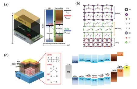
Solution-processed ETL contains defects originating from oxygen vacancies on the surface. The lattice mismatch between ETL and perovskite may generate a dangling bond at the interface. Uncoordinated sites can induce deep-level defect states in the bandgap, leading to poor charge transport and charge recombination. Interfacial engineering and trap state passivation at ETL/perovskite interface are essential.Seoket al. recently introduced an atomic-scale interlayer (FASnClx) to SnO2/perovskite interface through coating Cl-containing FAPbI3precursor solution onto Cl-bonded SnO2layer[2](Figs. 2(a) and 2(b)). The interlayer effectively passivates interfacial defects and boosts electron transport, yielding the record PCE of 25.5%. To achieve better energy level alignment with perovskite and reduceVocdeficit, many inorganic compounds have been introduced to tune the energy level of ETL. Kimet al.found that the introduction of Li-salt dopants(e.g. LiTFSI, Li2CO3, LiCl, and LiF) could improve the electrical properties of ETLs and device performance[19](Fig. 2(c)).Li2CO3-doped mesoporous TiO2(mp-TiO2) presents deeper conduction band than pristine mp-TiO2and other Li-salt doped mp-TiO2, which facilitates electron injection to perovskite. A certified efficiency of 24.68% was delivered.

Fig. 2. (Color online) (a) Left, a regular PSC with an interlayer between ETL and perovskite layer. Right, the energy level diagram. The interlayer suppresses back-recombination of the extracted carriers (purple arrow) without disturbing carrier transport. (b) The formation of the interlayer (FASnClx) between perovskite and SnO2. Reproduced with permission[2], Copyright 2021, Springer Nature. (c) Schematic for the PSC with mp-TiO2 ETL doped with different Li-salts and the energy level diagram for pristine mp-TiO2 and various Li-salt-doped mp-TiO2. Reproduced with permission[19], Copyright 2021, Elsevier.
In short, the optoelectronic properties of inorganic ETMs and the interface between ETL and perovskite significantly affect PSC performance. The performance of inorganic ETLs can be improvedviainterface modification and element doping.
Acknowledgements
L. Xie thanks High-Level Talents of Yunnan University(CZ21623201). Y. Hua thanks the National Natural Science Foundation of China (22065038), the Key Project of Natural Science Foundation of Yunnan (KC10110419), High-Level Talents Introduction in Yunnan Province (C619300A010), the Fund for Excellent Young Scholars of Yunnan(K264202006820), and the Program for Excellent Young Talents of Yunnan University and Major Science (C176220200). L.Ding thanks the National Key Research and Development Program of China (2017YFA0206600) and the National Natural Science Foundation of China (51773045, 21772030, 51922032,and 21961160720) for financial support.
杂志排行
Journal of Semiconductors的其它文章
- In-situ/operando characterization techniques for organic semiconductors and devices
- Frontier applications of perovskites beyond photovoltaics
- Comprehensive, in operando, and correlative investigation of defects and their impact on device performance
- Study of structure-property relationship of semiconductor nanomaterials by off-axis electron holography
- In-situ monitoring of dynamic behavior of catalyst materials and reaction intermediates in semiconductor catalytic processes
- Structural evolution of low-dimensional metal oxide semiconductors under external stress
