Self-organized TiO2 Nanotube Arrays with Controllable Geometric Parameters for Highly Efficient PEC Water Splitting①
2022-03-12WANGTianMingCHENYanXinTONGMeiHongLINShiWeiZHOUJingWenJIANGXiaLUCanZhong
WANG Tian-Ming CHEN Yan-Xin TONG Mei-Hong LIN Shi-Wei ZHOU Jing-Wen JIANG Xia LU Can-Zhong
a (CAS Key Laboratory of Design and Assembly of Functional Nanostructures, and Fujian Provincial Key Laboratory of Nanomaterials, Fujian Institute of Research on the Structure of Matter,Chinese Academy of Sciences, Fuzhou 350002, China)
b (College of Chemistry and Materials Science, Fujian Normal University, Fuzhou 350007, China)
c (Xiamen Institute of Rare-earth Materials, Haixi Institutes,Chinese Academy of Sciences, Xiamen 361021, China)
ABSTRACT In this report, a series of self-organized TiO2 nanotube arrays were prepared by anodization of titanium foil in mixed electrolytes composed of water, ethylene glycol, and NH4F. Their photoelectrochemical(PEC) performance as a photoanode was characterized by the PEC water-splitting hydrogen (H2) generation reaction. The internal relationship between the TiO2 nanotube arrays (TNTAs) morphology and their PEC performance was thoroughly investigated. Our results show that when the etching time is 10 hours, the length of the as-prepared TNTAs is about 20.78 μm and the measured photocurrent density is around 1.25 mA·cm-2 with applied bias voltage 0.6 V (vs. Ag/AgCl) under simulated sunlight irradiation, which is 976 times higher than that of the TiO2 substrate without nanotubes architecture (0.00128 mA·cm-2). More interestingly, the results of the IPCE measurement show that the band-gap of the as-prepared TNTAs is reduced from 3.20 to 2.83 eV. The corresponding optical response limit is also extended from 400 nm to TiO2 nanotube arrays is 510 nm, which indicates that the increasement of the TNTAs PEC performance benefits from the great improvement of its utilization of both the UV and visible light irradiation.
Keywords: photoelectrochemistry, water-splitting, TiO2 nanotube arrays, H2;
1 INTRODUCTION
The photoelectrochemical (PEC) water-splitting has been considered as one of the most promising approaches for solar-to-hydrogen (STH) since it was discovered by Fujishima and Honda in 1972. Among a variety of the materials developed for PEC applications, titanium dioxide(TiO2) is the most promising one due to its high efficiency,low cost, chemical inert, and photostability[1-3]. The photoactivation of TiO2has been extensively investigated.However, the large band-gap and the fast recombination of photo-generated carriers of bulk TiO2lead to a decreased efficiency of its solar utilization. Great efforts have been made to enhance the absorption of visible light and the rapid transfer of photo-generated carriers to achieve high efficiency STH. It was found that a rational TiO2architecture with large internal surface area, good electrical transport, low charge carrier recombination losses and intimate contact between the semiconductor and the electrolyte can effectively improve the performance of TiO2in the solar assisted PEC water-splitting.TiO2nanotubes (TNT) and TiO2nanotube arrays (TNTAs)provide unique electronic properties, such as high surfacesurface-to-volume ratios and sizedependence properties,obvious quantum confinement effect and high electron mobility for PEC water splitting. The discovery of TNT with various interesting properties has stimulated the quest for the synthesis of TNT structures. Several recent studies indicate that titania nanotubes have improved properties compared to any other form of titania for the applications in photocatalysis[4-6], sensing[7-10], photoelectrolysis[9-11]and photovoltaics[12-14]. TNTA and TNTAs can be produced by a variety of methods, including deposition into a nanoporous alumina template[15-18], sol-gel transcription using organo-gelators as templates[19-20], seeded growth[21], hydrothermal processses[22-24]and electrochemical anodization. Among all the aforementioned nanotube fabrication methods, the method of highly ordered nanotube arrays made by the anodization of titanium in fluoride-based baths[25-31]has been demonstrated to have the most remarkable properties as the dimensions of TNTA and TNTAs can be precisely controlled. Uniform titania nanotube arrays with various pore sizes (22~110 nm),lengths (200~6000 nm), and wall thicknesses (7~34 nm)can be easily obtained by adjusting electrochemical conditions. Many literature reports[33-38]have given evidence of the unique properties and huge performance improvement of this material architecture method, which make it of considerable interests in both scientific researches and practical applications.
In this work, a series of one-dimensional ordered TNTAs with different geometry parameters were prepared and their corresponding quantum efficiency and PEC performance as a photo-anode were characterized. Compared to the bulk TiO2substrate (0.00128 mA·cm-2at 0.6 Vvs.Ag/AgCl), the as-prepared TNTAs with 20.78μm tube length present about 1.25 mA·cm-2photocurrent density with applied bias voltage 0.6 V (vs. Ag/AgCl) under the simulated sunlight irradiation,showing a huge performance improvement. Our results imply that with the thickness of TNTAs lowing and the diameter of the TNT increasing, the absorption threshold of the TNTAs red-shifted to visible light.

Fig. 1. Schematic illustration of the preparation process of TNTAs by secondary anodization
2 EXPERIMENTAL
2. 1 Materials synthesis
TNTAs were fabricated by secondary anodization (Fig. 1).Firstly, the Ti foil (99.0%) substrates were polished by emery paper up to 2500 mesh and were sonicated in an acetone ultrasound bath (KUNSHAN ULTRASONIC INSTRUMENT CO., LTD) followed by washing in soap solution and deionized water (Millipore water, 18 MΩcm) for 2 mines each and drying under nitrogen stream to remove the stains and the slight scratches on their surface. The pretreated titanium foils were then anodized at a constant potential of 60 V in a fluorinated glycol organic solution, which is composed of 0.35 wt% NH4F and 1.6 vol% H2O at 20 ℃ and in dual parallel electrode configuration with a titanium mesh cathode for 1 hour as the first step anodization. Before the secondary anodization, the TNTAs template was removed by ultrasonic treatment of the electrode in water for 30 min. Ti substrate without secondary etching was named as TNT-B as a reference group. The secondary electrochemical anodization etching was set at room temperature with 60 V for 1 hour(TNT-1), 6 hours (TNT-6), and 10 hours (TNT-10), respecttively. The anodized electrodes were then annealed by heating to 400 ℃ (0.8 ℃·min-1) in the air for 2 hours. After completing the heating and temperature holding process,TNTAs samples were cooled to room temperature naturally in the air.
In a typical electrochemical anodization process, the titanium metal foil was used as an etching anode, and the thickness of the surface oxide layer gradually increases during the oxidation process. A dense oxide film was formed on the surface of the titanium metal sheet, and the fluorinecontaining organic solution dissolved the oxide layer to form a fluoride ion metal complex ([TiF6]2-), which diffused along the etched pipe into the solution and finally formed an ordered array of TiO2nanotubes under an applied electric field.
2. 2 Materials characterization
The structure and morphology of the prepared TNTAs sample were characterized by a field emission scanning electron microscope (FE-SEM) operating at 2.0 kV equipped with field emission (Apreo SLoVac). The crystal phases and structures of as-prepared TNTAs was characterized by X-ray diffraction (XRD) on Rigaku Miniflex 600 X-ray diffratometer system, equipped with CuKα(λ= 0.15406 nm)radiation, which was scanned over the angular range of 20~80° (2θ) with a scanning speed of 5 °·min-1. Micro structural examinations were conducted on JEOL JEM-2100 transmission electron microscopy (TEM) operated at 120 kV.
2. 3 Photoelectrochemical measurements
The photocurrent density was measured with a CS350 electrochemical analyzer (Wuhan Corrtest Instrument Corp.,Ltd, China) in a standard quartz made three-electrode cell in a 0.1 M Na2SO4aqueous solution (pH = 7), in which the TNTAs is the working electrode, a Pt foil is a counter electrode and a Ag/AgCl (saturated KCl) is the reference electrode. A 300 W Xenon Lamp equipped with filter(AM1.5G) and power density 100 mW·cm-2(PLS-SXE300D,Beijing Perfectlight Technology. Co., Ltd.) was used as an illumination source. The measured potentialvs.Ag/AgCl was converted to the reversible hydrogen electrode (RHE)according to the Nernst equation (1):

WhereE0(vs.RHE) = 0.1976 V at 25 ℃. The photocurrent reaction and incident photon to electron conversion efficiency(IPCE) spectra were obtained under the incident light with wavelength of 300~600 nm and intensity density of about 100 mW·cm-2using a monochromator. IPCE was calculated from chronoamperometry measurements recorded photocurrent density, using the following equation (2):

It is calculated as a function of the output photocurrent density (Iph, A·cm-2) and incident light power density (Pin,W·cm-2) at each wavelengthλ(nm).
Linear sweep voltammetry (LSV) was measured with a voltage scan speed of 0.005 V·s-1, and the light was chopped by a shutter of 5 s-1. LSV test conditions were consistent with IPCE. In general, the applied bias photo-to-current efficiency(ƞ) can be determined by equation (3).ƞrepresents the photoelectric conversion efficiency of a photoelectrode under an applied bias from a potentiostat.

whereJphis the photocurrent density of photoelectrode measured under applied voltage,Eappmeans the applied bias potential between the working electrode and counter electrode, andPlightis the incident simulate sunlight power input.
The Mott-Schottky measurement results were used to illustrate the flat band potentials, which were usually equivalent to the position of the semiconductor conduction band. The frequency range of the electrochemical analyzer is 0.01~100000 Hz, the voltages increment is 0.005 V, and the AC amplitude is 10 mV. The working electrode was measured at 500, 1000, 1500, 2000, and 2500 Hz,respectively. The Schottky barrier can be used to express the position of the conduction band potential and calculate the flat band potential energy. The calculation expression of the Mott-Schottky model using parallel plate capacitors is as the following equation (4):

In the parallel plate capacitor model,Cscrepresents the space charge layer capacitance,ɛmeans the inherent dielectric constant of semiconductors,ɛ0is the dielectric constant in vacuum,NDstands for carrier concentration,Eapplis the applied bias voltage,EFBis the flat band potential, andkis the Boltzmann constant andTsignifythermodynamic temperature.
3 RESULTS AND DISCUSSION
FE-SEM and TEM were used to investigate the structure and morphology of the TNTAs. Fig. 2 shows the TNTAs samples with different tube lengths and pore diameters, as well as the Ti substrates with the surface arrays removed (Fig.2a). The top view and the side view of TNT-1, TNT-6 and TNT-10 are shown in Fig. 2b, 2c and 2d, respectively.Obviously, with the anodization time increasing, the length of the nanotube gradually increases from 3.422 to 20.78and the diameter increases from 52.35 to 102.35 nm. This effectively increases the effective reaction area between photocatalysis and water. Simultaneously increases the absorption efficiency of light, which greatly improves the light conversion efficiency of TiO2. Fig. 2e and 2f are the high resolution transmission electron microscope (HRTEM)of the TiO2nanotube (TNT-6). The lattice spacing of 0.36 nm observed in the TNTAs samples is consistent with the lattice spacing of TiO2(101).

Fig. 2. SEM images of TNT-B (a), TNT-1 (b) , TNT-6 (c) and TNT-10 (d); TEM image (e) and HRTEM image (f) of TNT-6
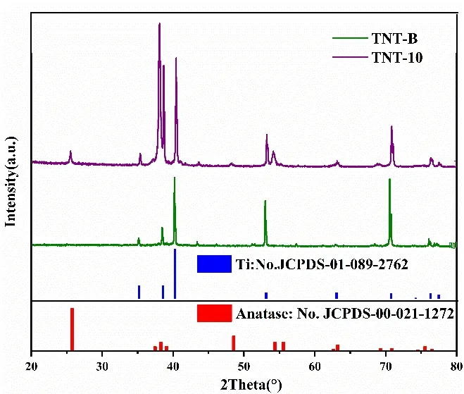
XRD patterns of the two TNTAs samples (TNT-10 and TNT-B) are shown in Fig. 3, which show that there are characteristic diffraction peaks of anatase TiO2at 2θ= 25.15°(101), 37.38° (004), and 47.78° (200). Obviously, the as-prepared ordered TNTAs are anatase, and the other appearing peaks come from the background of metallic titanium.

Fig. 3. X-ray diffraction patterns of ordered TNTAs
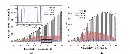
To better understand the synergistic effect of TNT architecture, systematic photoelectrochemical measurements were carried out on PEC anodes of TNT-B, TNT-1, TNT-6,and TNT-10, respectively. As shown in Fig. 4a, the measured photocurrent density of TNT-10 sample is around 1.25 mA cm-2with applied bias voltage 0.6 V (vs.Ag/AgCl) under simulated sunlight irradiation, which is 976 times higher than that of the TiO2bulk substrate (TNT-B: 0.00128 mA cm-2).Furthermore, with the increase of the length of the ordered TNT, its measured photocurrent density increases as well, for example, the photocurrent density of the TNT-6 array is about 0.38 mA cm-2, the photocurrent density of the TNT-1 nanotube is about 0.06 mA cm-2. Fig. 4b shows the total percent photoelectric conversion efficiency (η) of TNT-10,TNT-6, TNT-1 and TNT-B under simulated sunlight irradiation. A maximum photoconversion efficiency of 1.03 %was observed at an applied potential of 0.6 Vvs.Ag/AgCl for the TNT-10 nanotube array sample, while it was only 0.01 %for the TNT-B at 0.6 Vvs.Ag/AgCl.

Fig. 4. Linear sweep voltammogram (LSV) curves (a) and their corresponding photoelectric conversion efficiencies (b) of different nanotube arrays
As shown in Fig. 5, the photocurrent densities of different TNTAs PEC-anodes were measured under monochromatic light irradiation. In addition, the incident monochromatic photon to current conversion efficiency (IPCE) can be given as a function of wavelength (k) as shown in equation (2).

Fig. 5. Comparisons of different TNTAs samples at electrochemical noise mode (top) and at 0.6V applied voltage (vs. Ag/AgCl)mode (bottom): photocurrent density (a, b), the derived IPCE (%) spectra (c, d), and the band gap determination extracted from IPCE spectra by a function of (IPCE% × h)1/2 vs. h (e, f)
In particular, with the tube length of the as prepared TNTAs increases, the measured photocurrent density obtained with or without bias applied potential increases significantly, see Figs. 5a and 5d. The maximum photocurrent density of TNT-10 (19μA· cm-2at 365 nm) is around 1.5, 2 and 3.8 times higher than that of TNT-6 (12.6μA·cm-2at 360 nm), TNT-1(9.5μA·cm-2at 355 nm), and TNT-B (5μA·cm-2at 345 nm), respectively. Furthermore, with the increase of the length of the nanotube the TNTAs samples show a significant photo response red-shift in the wavelength range of 400~480 nm. All of these results give the insight that the TNTAs architecture highly enhances the PEC activity of the TiO2under both UV and visible light regions.
In order to deeper understand the interplay between the photocatalysis and the light absorption of four types of different length TNTAs, IPCE measurements were performed under monochromatic light irradiation. As shown in Fig. 5b,the maximum IPCE of TNT-10 obtained in the electrochemical noise mode (without any applied voltage) is around 28.89% at 354 nm. That is higher than that of the TNT-6 (17.66% at 353 nm), TNT-1 (15.52% at 350 nm) and TNT-B (9.7% at 350 nm). In addition, as shown in Fig. 5e,when 0.6 V (vs. Ag/AgCl) bias potential was applied on the TNTAs PEC anode, the peak IPCE of TNT-10 shifts to 42.98%at 355 nm, which is higher than that of the TNT-6 (37.91% at 354 nm), TNT-1 (33.82% at 352 nm) and TNT-B (21.99% at 350 nm). Meanwhile, the wavelength response cut-off range of TNT-10 red-shifts to 500 nm, see the inset curve in Fig.5(e).
In comparison with the four samples, it indicates that the UV and visible lights are effectively used for STH, in which the absorption and transportation of photogenerated charge carriers were as efficient as the nanotube arrays, with the increase of the length and diameter. The band gaps of samples can be evaluated from the IPCE spectra by a Tauc plotting (IPCE% ×hυ)1/2versus photon energy (hυ)[39,40]as shown in Fig. 5c. The extracted band gaps of TNT-10, TNT-6,TNT-1 and TNT-B were found to be 3.04, 3.10, 3.15, and 3.20 eV at electrochemical noise measurement. Fig. 5f illustrates that the obtained band gaps were narrowed, which were 2.83, 2.88, 3.01, and 3.20 eV at 0.6 Vvs.Ag/AgCl.Interestingly, when the nanotube array exists, with the application of external voltage, the band gap gradually narrows. This phenomenon implies that the modification of TiO2nanotubes from both the morphology and the semiconductor band gap is very successful.
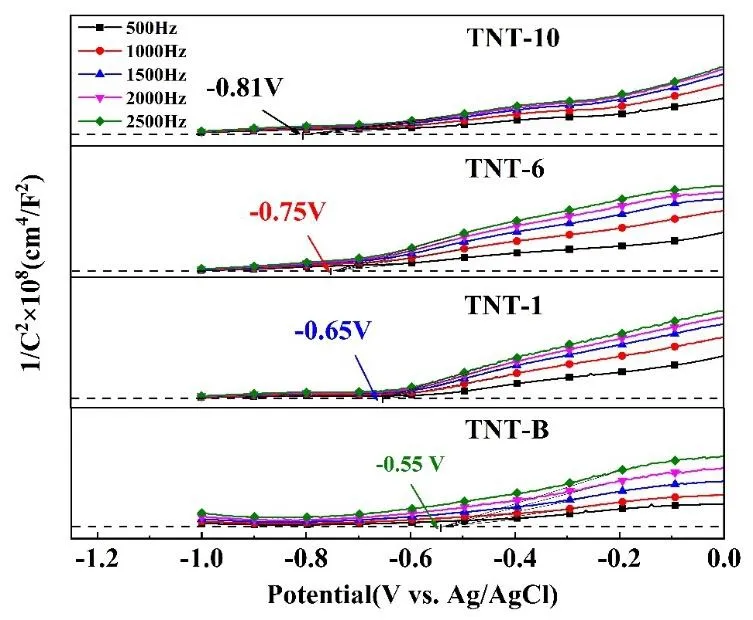
The Mott-Schottky measurements were employed to evaluate the flat band potentialVfbof TNTA electrodes with different tube lengths, which as shown in Fig. 6.

Fig. 6. Mott-Schottky plots of different TNTAs.
The Mott-Schottky plots of the TNTAs and base exhibited a positive slope, which indicates that both electrodes aren-type semiconductors. Additionally, as the length of the nanotube increases, the flat-band potential of the nanotube array shifts negatively, which is conducive to hydrogen
production. TheVfbof TNT-10, TNT-6, TNT-1 and TNT-B were observed at
-0.81 V, -0.75 V, -0.65 V and -0.55 Vvs.Ag/AgCl,respectively. The flat potential (in the units of volts, V) can be referred to the position of the conduction band (in the units of electron volts, eV)[41,42]. Thus, as the length of the nanotube increases, theEfbshifts negatively, which is beneficial to the PEC water splitting.
Based on the above results, we proposed the band structures of the as prepared TNTAs samples, TNT-B, TNT-1,TNT-6, and TNT-10 respectively, as shown in Fig. 7. As we can see, the length of TNT varies from 0 to 20.78μm, the band gaps gradually narrows from 3.24 eV to 3.04 eV, and the photo-response wavelength limits from 400 to 480 nm.

Fig. 7. Proposed band structure of TNTAs samples with different tube lengths and redox potentials for water splitting.Black and green dotted lines represent valence band of TNT-10 and TNT-B respectively.
4 CONCLUSION
In summary, the one-dimensional ordered TNTAs show a greater improvement in the light absorption range, and with the length of the nanotube increases, its absorption threshold red-shifted to visible light. By carefully investigated the internal relationship between the TiO2nanotube arrays(TNTAs) morphology and their PEC performance, we proved that when the anodization time goes to 10 hours, the length of the as prepared TNTAs is about 20.78 μm. The measured photocurrent density is around 1.25 mA cm-2with applied bias voltage 0.6 V (vs. Ag/AgCl) under simulated sunlight irradiation, which is 976 times higher than that of the TiO2bulk substrate (0.00128 mA cm-2). More interestingly, the results of the IPCE measurement show that the band-gap of the as prepared TNTAs is reduced from 3.20 eV to 2.83 eV with applied bias voltage 0.6 V (vs. Ag/AgCl). The corresponding optical response limit is also extended from 400 nm to 510 nm, which implies that the increase of the PEC performance of the TNTAs is due to the great improvement of the utilization of both UV and visible light irradiation. Our findings show that the unique ordered nanotube array structure can further improve the response of TiO2to light under the action of a small applied bias, which is of great significance for electro-optic synergistic catalysis.
杂志排行
结构化学的其它文章
- Synthesis, Crystal Structure and Fungicidal Activity of 3,4-Dichloro-5-(6-chloro-9-(4-fluorobenzyl)-9H-purin-8-yl)isothiazole①
- Synthesis, Crystal Structure and Antifungal Activity of New Furan-1,3,4-oxadiazole Carboxamide Derivatives①
- Syntheses, Crystal Structures, Anticancer Activities and DNA-Binding Properties of the Dibutyltin Complexes Based on Benzoin Aroyl Hydrazone①
- Synthesis, Crystal Structure, Fungicidal Activities and Molecular Docking of Acyl Urea Derivatives Containing 2-Chloronicotine Motif①
- Molecular Design and Property Prediction of High Density 4-Nitro-5-(5-nitro-1,2,4-triazol-3-yl)-2H-1,2,3-triazolate Derivatives as the Potential High Energy Explosives①
- A New Borate-phosphate Compound CsNa2Lu2(BO3)(PO4)2:Crystal Structure and Tb3+ Doped Luminescence①
