Topological circuit:a playground for exotic topological physics
2021-09-03LIUShuoZHANGShuangCUITiejun
LIU Shuo,ZHANG Shuang,CUITie-jun*
(1.School of Physicsand Astronomy,University of Birmingham, Birmingham B15 2TT,United Kingdom;2. State Key Laboratory of Millimeter Waves,Southeast University, Nanjing 210096,China;3. Department of Physics,The University of Hong Kong, Pokfulamroad 999077, Hong Kong,China)
Abstract:Exploring topological phases of matter and their exotic physicsappeared asa rapidly growing field of study in solid-state electron systems in the past decade.In recent years,there has been a trend on the emulation of topological insulators/semimetals in many other systems,including ultracold quantum gases, trapped ions, photonic,acoustic,mechanical,and electrical circuit systems. Among these platforms,topological circuitsmade of simple capacitive and inductive circuit elements emerged as a very competitive platform because of its highly controllable degrees of freedom,lowercost,easy implementation,and great flexibility for integration.Owing to the unique advantages of electrical circuits such as arbitrary engineering of long-range hopping,convenient realization of nonlinear,nonreciprocal, and gain effects,highly flexible measurement,many of the nonlinear, non-abelian,and non-Hermitian physics can be potentially realized and investigated using the electrical circuit platform.In this review,we provide the first short overview of the main achievements of topological circuitsdeveloped in the past six years, primarily focusing on their theoretical modeling,circuit construction,experimental characterization,and their distinction from their counterparts in quantum electronics and photonics.The scope of this review covers a wide variety of topological circuits,including Hermitian topological circuits hosting nontrivial edge state, higher-order corner state,Weyl particles;higher dimensional topological circuits exhibiting nodal link and nodal knot states;non-Hermitian topological circuits showing skin effects,gain and loss induced nontrivial edge state;self-induced topological edge state in nonlinear topological circuit;topological circuit having non-Abelian gauge potential.
Key words:topological insulator;topological semimetal;electrical circuit;edge stage; bulk-edgecorrespondence
1 Introduction
Topological Insulators(TIs)and semimetals are special types of materials that host nontrivial topologiesin the bulk band structure and show topologically protected edge statesat the boundary[1-2].Unlike normal insulators,TIs are insulating(or semiconducting)in their interior,but conducting on their surface[3].Although topological materials originate from condensed matter physics,they have attracted enormous attention from researchers in many other fields,and have been emulated in various systems such as photonic[4-5],acoustic and mechanical[6],and electrical circuit systems[7-8].Among these systems,electrical circuits are emerging as an ideal experimental platform for emulating topological effects,as they show much higher flexibility in implementing desired hopping,gain and loss,nonreciprocity and even nonlinearity.The wide variety of circuit devices allows direct mapping from tight-binding modelsto electrical circuits, thus enabling the realization of many novel topological systems with non-Hermitian, nonlinear, non-abelian effects,which are extremely challenging to implement in quantum systems.
Although the research on topological circuits only began in 2015[9],they have evolved rapidly and have covered almost all types of topological insulators/semimetals from Hermitian to non-Hermitian,from one dimension to four dimensions,from linear to nonlinear,from abelian to non-abelian.In this review,we attempt to summarize the development of topological circuits made over the past six years,mainly focusing on the theoretical modeling,circuit realization and experimental characterization.The intention of this review is to build bridges between research communities in electrical engineering and condensed matter physics, thus helping motivate more explorations on exotic topological physics in electrical circuits,and stimulating inter disciplinary collaboration on the practical application of topological circuits.
Before westart reviewing the progresson topological circuits,it is important to clarify several major differences on the design of topological insulators in electrical circuits and that in the condensed matter and photonic systems.The first difference is the theoretical formulation of band topology of circuit.The Hamiltonian for a circuit derived from Kirchhoff equations cannot always be directly mapped to the tight binding Hamiltonian established in condensed matter system,except for a few simple cases when the basis can be reduced to only the voltage set or current set,which are the voltage on every node and current through every branch,respectively.This is because for a circuit withNnodes, the natural Hamiltonian with eigenvalue ofωis written in the basis containing both voltage and current sets.Hence,the dimension of circuit Hamiltonian is doubled as compared to that of the tight binding Hamiltonian for the condensed matter system.However,one can always obtain the circuit Laplacian,also known as the admittance matrix(or the inverse of impedance matrix)in electrical engineering, whose basis is equal to the number of independent nodes in the circuit.The circuit Laplacian takes exactly the same form as the tight binding Hamiltonian in condensed matter system.However,it is important to note that circuit Laplacian is a function ofω,and therefore its eigenvalue does not correspond to the circuit eigenfrequency.The eigenfrequencyωcan either be obtained by solving the roots of the determinant of circuit Laplacian,or by solving the circuit Hamiltonian that is built from the capacitance,inductance and conductance matrices[10-11]. Alternatively,one can also obtain the circuit Hamiltonian by applying Euler-Lagrange(EL)equation of motion to the circuit Lagrangian[12],which avoid analyzing the circuit from the perspective of Kirchhoff equations.
Another difference that should be noticed for topological circuit is its boundary termination.A natural boundary truncation of the circuit is by simply cutting the circuit at the coupling term(i.e.discard the coupling term).However,thisconfiguration does not lead to the same boundary as in the condensed matter and photonic systems,because the coupling terms also contribute to the onsite term in the circuit Laplacian.Therefore, the removal of boundary coupling terms will result in changes in the onsite potential at the boundary sites,and thus affecting the existence of topological edge state.To solve this issue,additional grounding terms should be added to the boundary sites to maintain an identical onsite potential with that of the bulk sites.
Experimental characterization of topological circuits is also different from the photonic systems,including the measurement of topological edge state and band structure.The topological edge stage in electrical circuit is manifested by either the voltage on the node,current through the branch,or the impedance between neighboring nodes,depending on the basis chosen for the circuit Hamiltonian or the circuit Laplacian.For example,if the circuit Hamiltonian is written in the basis of only the voltage set or current set,the edge states as well as bulk states can be measured with an oscilloscope through the voltage across all nodes,or current flowing through all branches.In this configuration,the circuit needs to be excited by an external AC source,which can be done by either driving one of the circuit node through a resistor connected in series,or by inductively coupling the inductors with a driving coil[9].These two approaches tend to be equivalent when the value of the series resistor becomes infinity.However,maintaining an identical coupling coefficient for all measurements ischallenging for the inductive coupling approach.Besides,the AC source and oscilloscope need to be programmed to obtain the voltage/current spectrum.Alternatively,one can always access the full information of the circuit through the impedance spectra between every two neighboring nodes,which can be obtained by measuring the S-parameter matrix of the circuit using a Vector Network Analyzer(VNA)[13]. This method is more convenient and also reliable,allowing us to obtain the information of the topological edge state[10],the Local Density Of States (LDOS)[14],as well as the band structure of the circuit[15].
2 Topological edge states in passive topological circuits
Ref.9 represents one of the earliest works on topological circuit.In this work,Jia et al.demonstrated a spin-dependent topological edge state in a two-dimensional circuit lattice implemented with a network of inductors and capacitors(Figure 1a).The voltage across the two inductors within each unit cell was used to construct the pseudo spin degree of freedom.The hopping among neighboring unit cells was realized through a capacitor network with four different wire braidings as shown in Figure 1b,which is equivalent to four coupling phases of 0,π/2, π,3π/2.The gradient phase hopping along they-direction provides the circuit with π/2 flux per plaquette, which generated a spin-dependent topological edge state that propagated unidirectionally along the circuit boundary.The circuit was excited by inductively coupling a certain inductor using a 5-turn 8-mm diameter driving coil,and the edge state was detected by inductively probing the voltage acrossall theother inductors with a pickup coil.
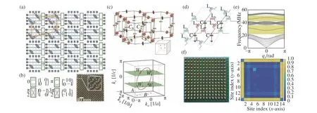
Fig.1 (a-b)Spin-dependent topological edge state in an electrical circuit mimickingπ/2 flux Hofstadter model[9].(c)3D topological circuit with topological nodal line stateand Weyl state controlled by the circuit parameters[16].(d-f)Two-dimensional version of the Su–Schrieffer–Heeger model circuit[17].图1 (a-b)具有π/2感应强度的Hofstadter 电路模型中的自旋依赖的拓扑边界态[9]。(c)三维拓扑电路中受电路参数调控的拓扑节线态和外尔态[16]。(d-f)二维形式的Su–Schrieffer–Heeger 拓扑电路[17]。
In 2018,Luo et al. presented a 3D circuit design that hosted topological nodal line state and Weyl state,and showed that they could be controlled by the circuit parameters[16]. The circuit was directly mapped from the tight binding Hamiltonian by engineering each site with an LC resonant tank and a hopping mechanism via capacitors(Figure 1c). Note that unlike the circuit design in Ref.9 which did not have a common ground,all circuit nodes in this work shared a common ground,which facilitated measurement using VNA.The circuit exhibited a nodal ring in the3D momentum space with a specific interlayer connection,which further degenerated into four Weyl points with an extra interlayer that broke the inversion symmetry.
In 2019, Liu et al. experimentally demonstrated a nontrivial edge state in a two-dimensional version of Su–Schrieffer–Heegermodel circuit[17],as shown in Figure 1d,in which each unit cell was composed of four grounded capacitors connected through alternating inductors in thexandydirections.Figure 1e shows the band structure of the circuit with closed boundary condition alongx-axis and open boundary condition (OBC)alongy-axis.Two isolated curves residing in the bulk band gaps represent the nontrivial edge states, which are characterized by the extended Zak phase(π,π).The topological edge state was manifested in experiment as pronounced absorption at the circuit boundary of the sample with 7.25×7.25 unit cells(Figure 1f), based onS11measurement at every circuit node using VNA.The authors also tested the robustness of the topological edge state with several different transmission measurements under different levels of circuit disordersand defects.
3 Ideal Weyl particles in topological circuit
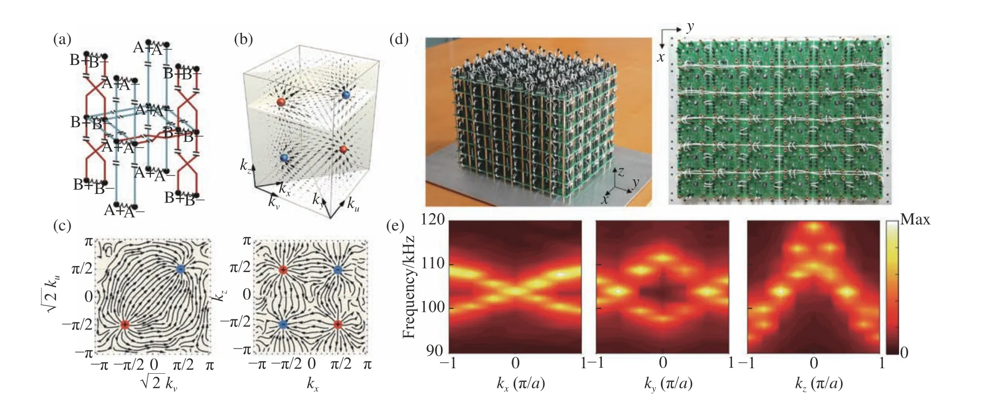
Fig.2 (a-c)Experimental observation of WPs in a 3D circuit lattice built with inductors and capacitors[15].(d-e)Experimental observationof ideal type-II WPs realized in a 3D topological circuits[23].图2 (a-c)由电容和电感构成的三维拓扑电路中的外尔点的实验观测[23]。(d-e)三维拓扑电路中的理想II型外尔点的实验观测[23]。
Weyl particles(WPs),also known as Weyl degeneracies or Weyl fermion,are solutions to the massless Dirac equation derived by Hermann Weyl,and have been demonstrated in the form of quasiparticles in condensed matter system and photonics[18-21].The Weyl points come in pairs in the three-dimensional momentum space with opposite chiralities, which are counter-parts of magnetic monopoles having positive and negative charges in real space.Hence,WPs gain a nontrivial topological invariant (Chern number),and exhibits chiral surface state at the materials surface that connect between the projections of WPs of opposite topological charges on the surface.The exotic features of WPs have aroused a great interest in its experimental observation in semimetals[18-19].Due to the stringent symmetry requirement of ideal WPs in which all the WPs are located at exactly the same energy/frequency, there have been very few reports on the realization of ideal WPs in bosonic or fermionic systems[20-22].
In 2019,Lu et al. reported the experimental observation of ideal WPs in a 3D circuit lattice built with inductors and capacitors[15].The unit cell takes the form of a half-flux Hofstadter model with π phase threading each plaquette,as shown in Figure 2a.By calculating the 3D band structure from the tight-binding Hamiltonian, the authors found in the momentum space the existence of four ideal WPs atk=(−π/2,0,−π/2)as the degeneracies of two bands.The near-sphere equifrequency surface around the Weyl frequency further confirms the linear degeneracy nature of the WPs.
A bulk sample containing 8×8×8 unit cells was fabricated with opposite surfaces of the sampleconnected via ribbon cables to impose Periodic Boundary Condition(PBC).The authors successfully recovered the full 3D band structure in the experiment by inductively measuring the voltage at all circuit nodes using a home-made automatic probing device.This is almost impossible in photonic and electronic systems as we cannot probe into the bulk of rigid materials.Figure 2b and 2c show the extracted Berry curvature of the lower band,where the vector flow from sources to sinks demonstrated the existence of four ideal WPs with topological charges of ±1.The locations of the Weyl point matched well with theoretical predictions.The chiral charge of the WPs was evidenced by the direct detection of Fermi-arc surface states connecting their surface projections.The authors added that the use of ferrites allows realization of T-broken Weyl semimetals[22].
In another work,Li et al.experimentally demonstrated an ideal type-IIWPsystem in an electrical circuit[23], which was different from the type-I WPsystem proposed in Ref.15 in that the dispersion around the band crossings is strongly tilted,leading to nonzero density of states at the Weyl frequency.Type-II WP was first theoretically predicted in 2015[24],and has been experimentally confirmed in condensed matter[19,25],and photonics[26-27].However,there has been a lack of experimental realization of ideal Type-II Weyl semimetals,in which all WPs reside symmetrically at the same energy with a large momentum separation and are clean from the nontrivial bands.The Type-II WPs were realized by stacking two layers of LC resonate dimersin each unit cell with broken inversion symmetry and preserved time-reversal symmetry.Figure 2d showsthe assembled sample which contains eight layers of PCB,with all three boundaries connected inloop to mimic the periodic boundary condition.The band diagrams shown in Figure 2e wereexperimentally obtained by mapping the impedance spectra of all circuit nodes using VNA,and followed by a Fourier transform.The existence of type-IIWPs was experimentally verified at theoretically predicted locations in the momentum space,as are shown in different projection planes in Figure 2e.The topological surface state was also demonstrated by another sample with OBC along one direction.The authors remarked that Type-II WPs featuring strongly tilted cone spectra near the WPs might motivate the design of some realistic and innovativedevices,and could be employed to explore some fascinating analogues in astrophysics such as the Hawking radiation and gravitational lensing.
Two more works reported the design of topological circuit that could switch between Type-I and Type-II Weyl semimetal phases[28],and transmission across heterojunctions consisting of a Type I Weyl semimetal source to a drain in the Type II or intermediary Type IIIWSM phase[29].
4 Higher-order topological circuits exhibiting corner state
Most of the research interestsof topological insulators have focused on the observation of protected nontrivial edge mode localized at the material surface.Recent emergence of Higher-Order Topological Insulators(HOTIs)hasled to discoveriesof topological boundary states with dimensions lower than that of the bulk by more than 1[30-32]. These quantized higher order multipole corner states are localized at the intersection of edges of a square(2D,quadrupole moment)or cubic(3D,octupole moment)lattice,and are protected by specially designed spatial symmetries. In 2018, Imhof et al.presented an experimental observation of a quadrupole moment induced corner state in a 2D electrical circuit[33], based on the theory proposed by Benalcazar et al.in 2017[30].Each unit cell comprised of four resonators coupled via inductors or capacitors as shown in Figure 3a.The admittance of the capacitor and inductor branches were designed to have equal amplitude but opposite phases,so that each smallest loop experienced a π-phase flux.This is key to endow the circuit with anticommuting mirror symmetries along thexandyaxes,which forms a quadrupole moment in the bulk circuit that forces theedge state to appear at the corners of circuit lattice.Figure 3b shows the eigenvalue spectra of the circuit Laplacian,in which an isolated curve passing through zero admittance at the resonant frequency represent the corner state (Figure 3b).The topological corner state was experimentally confirmed through a distinct peak in the impedance spectrum obtained at one of the circuit corners,as shown in Figure 3c.
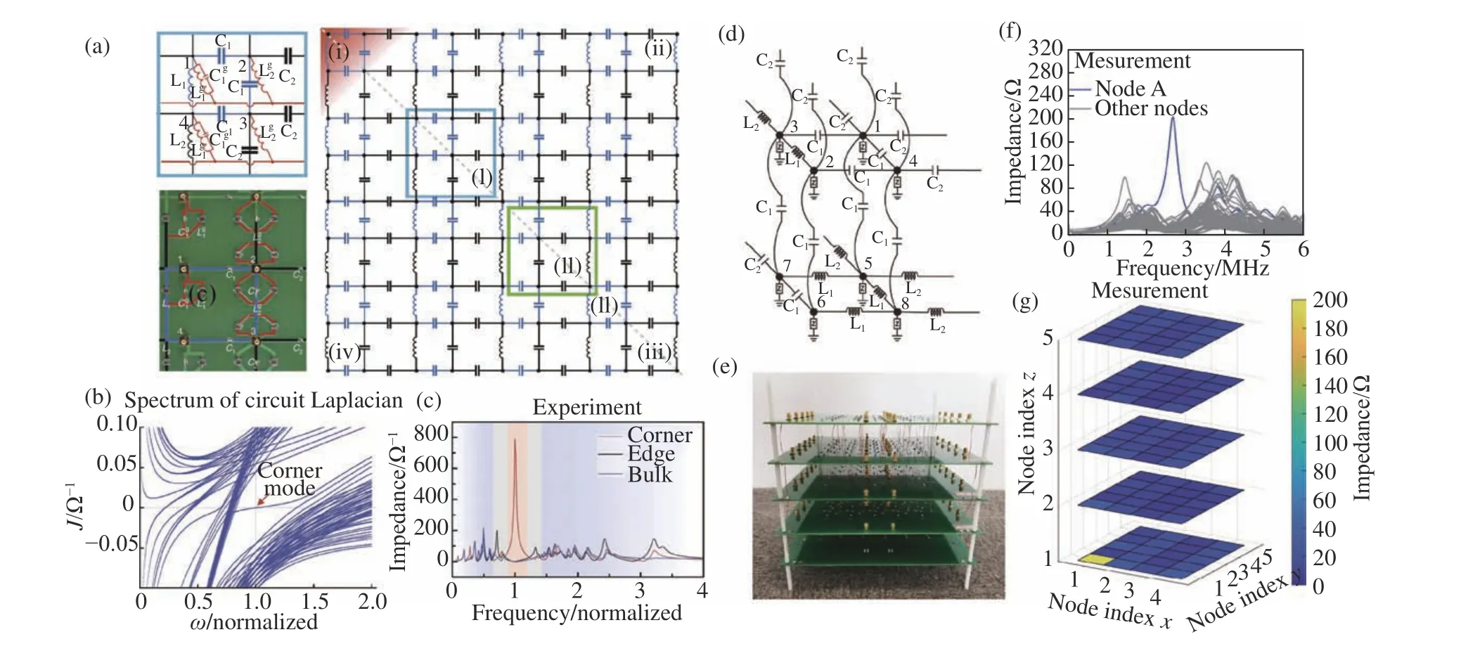
Fig.3 (a-c)Experimental observation of a quadrupolemoment induced corner statein a 2D electrical circuit[33].(d-e)3D topological circuit exhibiting 0D corner state topologically protected by octupole moment of the bulk circuit[34].图3 (a-c)二维高阶拓扑电路中由四极子动量导致的拓扑角模式的实验观测[33]。(d-e)三维高阶拓扑电路中由八极子动量所保护的零维拓扑角模式[34]。
In 2020,Liu et al.extended the concept to a 3D topological circuit which hosts0D corner state topologically protected by three anticommuting reflection symmetries of the bulk lattice[34].They verified that such corner state is induced by the nontrivial octupole moment of the 3D circuit,which was achieved by designing dimerized coupling along three axes and by letting each plaquette to have opposite sign to the other three,as illustrated in Figure 3d.They fabricated a sample that comprised of 2.5×2.5×2.5 unit cells using five layers of circuit board (Figure 3e),and measured the impedance spectra between every adjacent circuit node using VNA.A distinct peak was clearly identified from the impedance spectrum at exactly the corner mode frequency (Figure 3f),which was confirmed to be the octupole corner state(Figure 3g). Note that Ref.35 also reported a similar circuit for realizing octupole corner state in a 3D circuit.
HOTIs can also be realized by other means.In 2018,Ezawa proposed the circuit implementation for realizing Majorana-like corner states by applying an effective field on the Bernevig-Hughes-Zhang(BHZ) model[36].The square lattice circuit unit cell was composed of four resonators, whichwere coupled through LC components along thexdirection,and negative resistor modules along theydirection.The author found a pair of corner states residing at opposite corners of the 2D circuit lattice,which were detected by the emergence of the impedance resonance.As the evolution of the wave functions of corner states inherited the same braiding behavior of Majorana fermions,the author considered them to be Majorana-like corner states.
5 Four-dimensional topological circuit
Higher-dimensional topological insulators and superconductors,as theoretically predicted by the ten-fold classification of topological insulators[37],have attracted wide attention in condensed matter physics as they exhibit much richer physics than their 2D and 3D counterparts.For instance,Class AI TIs with four-dimensional (4D)configuration does not require any special spatial symmetries.However,as electrons can only move in three spatial dimensions, these hypothetical high-dimensional TIs cannot be realized with nature materials. Although there have been theoretical proposals for realizing high-dimensional TIs using synthetic dimensions[38-39],the extra dimensions do not physically exist but are some controllable parameters on the spatial degree of freedom,hence they do not support direct measurements of the topological edge states.Fortunately,it is possible to construct genuine higher-dimensional TIs with electrical circuits as each node supports unlimited number of connections to other nodes with arbitrary distances.
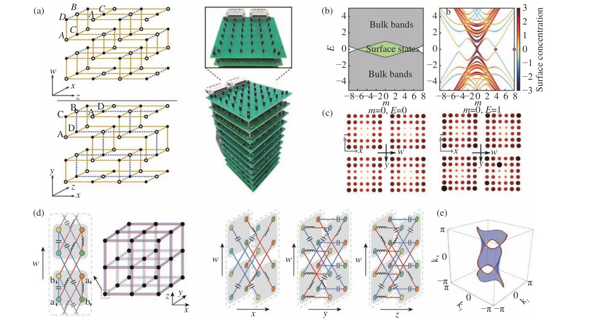
Fig.4 (a-c)Experimental implementation of the first 4D quantum Hall model in electrical circuit characterized by a nonzero second Chern number[40].(d,e)4D circuit topological circuit exhibiting a Seifert surface, which is 2D surface with its boundary tracing out a link or knot in 3Dmomentum space[41].图4 (a-c)具有二阶陈数的四维拓扑电路中的量子霍尔效应的实验验证[40]。(d,e)四维拓扑电路中的Seifert 表面,即三维动量空间中二维表面引出的节线或者节点[41]。
In 2020,Wang et al.experimentally implemented the first 4D quantum Hall model in electrical circuit which presents topological surface states that are characterized with a nonzero second Chern number but vanishing first Chern numbers[40].Figure 4a shows the circuit diagram of the unit cell,which contained four siteslabelled A,B,C,D connected to their nearest neighbors along all axis(x,y,z,w)through hopping parameter ±J.By adding longrange hopping in thex-zplane and masses to A/B sites,the circuit acquired a Class AI topological phase with T preserved.A 4D sample was fabricated which contained three unit cells in thexandzdirections,and one unit cell inyandw, with 16 bulk sites and 128 sites surface sites.Periodic boundary conditions were imposed on theyandwaxes.Figure 4b shows the band diagram of the finite circuit as a function of the mass detuning parameterm,which exhibits a nontrivial gap for |m|<6,with color indicating the level of localization of the energy state to the surface.The topological edge state was evidenced by the LDOS through impedance measurement at the edge mode frequency,as shown by Figure 4c.It is observed that the intensity of LDOS at the boundary sites is higher than those at the bulk sites.
At the same time,Yu et al. presented a 4D class AI TI in electrical circuit based on numerical simulations.They implemented the 4D circuit in a fully 2D layout,with LCresonators coupled through positive and negative capacitors.They observed surface Weyl states from the band structures obtained from Fourier transform of circuit transient simulations.They found that,as surface Weyl states with opposite charges resided on opposite surfaces of the 4D space,they could not be annihilated under slightly detuned onsite potential, but only experience certain shift in the momentum and frequency space.
Li et al. proposed in a 4D circuit lattice the emergence of Seifert surface, which is a 2D surface with its boundary tracing out a link or knot in 3D momentum space[41].These knotted structures lead to new phases of matter that are characterized by topological invariants in the form of polynomials rather than Z2and integers for ordinary TIs.As Seifert surfaces do not exist in 3D materials,they proposed to engineer such nodal links and nodal knots directly in 4D space, so that their projections onto the 3D subspace can form more complicated nodal linkages or knots. It isimportance to notethat,unlike in the 3D system,emergence of nodal links in 4D doesnot require any spatial symmetry.
Figure 4d shows the circuit diagram of the unit cell along thex,y,z,wdirections and overall circuit.Each unit cell contains four sites,which are connected to neighboring nodes through positive(red)and negative (blue)couplings realized with inductors and capacitors.By applying OBCalong thewdirection,they numerically obtained the Seifert surface of the2-link reconstructed from impedances across intra-unit cell diagonal sites as pronounced resonance peaks.The Seifert surface boundary forms two linked loops, which agree with analytical calculations.
6 Non-Hermitian topological circuit
Non-Hermitian topological systems are recently attracting increasing attention due to their novel topological phases and the breakdown of bulk-boundary correspondence[42-44]. Non-Hermitian systems involve gain/loss, or nonreciprocity,which bring new symmetries that require new topological classifications of bands[45]and new topological invariants[43,46-47].Experiments on non-Hermitian topological systems are challenging,as balanced gain and loss are difficult to be introduced in cold atoms or photonics.Recently, electrical circuits have emerged as an ideal platform for the experimental study of various non-Hermitian topological system due to the widechoicesof active devices.
Based on the theoretical work proposed by Takata[42],Liu et al. presented an experimental realization of a non-Hermitian electrical circuit whose nontrivial topology was induced by the introduction of gain and loss[48].The circuit contained a 1D array of LC resonators coupled with identical capacitors,with ordinary resistorsR1,R2,and negative resistors-R1,-R2connected in parallel with each LC resonator as shown in Figure 5a.The circuit exhibited four different phases for different combinations of the gain and loss settings(Figure 5b),which were characterized by the crossings among the four bulk bands.Three phases acquired a nonzero topological invariant, the normalized Berry phase,and exhibited nontrivial topological edge states.It is important to emphasize that,different from the theoretical model in Ref.42,an additional ordinary resistor functioning as a global loss term was added to all LC resonators in the circuit to guarantee a real-valued edge state.In addition, to provide stable working status for the operational amplifier,the imaginary part of most of the bulk modes were engineered to be negative(lossy).Experiments were carried out on the observation of edge states at the circuit boundary and interface state between two chains configured in different phases,which showed pronounced impedance peak at the edge mode frequency (Figure 5c).
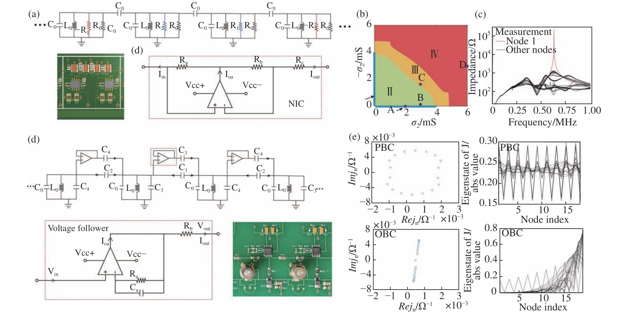
Fig.5 (a-c)Experimental realization of a non-Hermitian electrical circuit whose nontrivial topology is induced by the introduction of gain and loss[48].(d,e)Experimental observation of non-Hermitian skin effect in a variation of SSH topological circuit with nonreciprocity[13].图5 (a-c)由增益和衰减导致的拓扑相变的实验验证[48]。(d,e)具有非互易效应的非厄米拓扑电路中的趋肤效应的实验验证[13]。
Non-Hermitian systems also lead to some strange effects on the emergence of topological edge stage.In 2018,Yao et al. found the breaking of bulk-edge correspondence in non-Hermitian systems with nonreciprocity,and successfully solved this issue by assuming a non-Bloch wave number that take into account the gain and loss of the eigenstate[43].In 2021,Liu et al.demonstrated the non-Hermitian skin effect in a variation of SSH topological circuit with nonreciprocity[13], which was realized through the unidirectional coupling feature of voltage follower module(Figure 5d).By measuring theN-portS-parameter matrix using a two-port VNA,and then transforming it to the admittance matrix (circuit Laplacian),they experimentally confirmed the breakdown of the conventional bulkboundary correspondence by comparing the eigenvalue spectra of circuit Laplacian between the PBC and OBC.They observed that all the eigenstates oscillated in the entire chain with almost identical intensity under PBC,while decay exponentially from the circuit edge under OBC (Figure 5e). Note that another work by Helbig et al.also reported an experimental demonstration on the generalized bulk–boundary correspondencein non-Hermitian topolectrical circuits[49].
A few more works have been reported on the simulationsof non-Hermitian topological circuit,including the generation of higher-order corner states in a nonreciprocal circuit implemented with diodes[50],chiral edge states in a non-Hermitian Haldane model realized by voltage follower modules[51], bulk Fermi-arc states connecting the exceptional points and bulk drumhead states bounded by the exceptional lines in 2D and 3D non-Hermitian Honeycomb topological circuit[52].
7 Topological circuit with non-abelian topological gauge potentials
The mathematical structure of all the aforementioned topological circuits belong to the Abelian groups, with the topological charges being commutative and additive.That is,the number of edge states is strictly determined by the topological invariants(commonly as Z or Z2)of the material, as is governed by the bulk-edge correspondence.Most recently,topological system with non-abelian gauge potentials have received wide attention due to the unconventional properties such as trajectory-dependent Dirac node collisions,admissible nodal line configurations[53-56]and its potential applications in the implementation of fault-tolerant quantum computation[57].However, the construction of such non-Abelian topological systems requires noncommutative matrix-form gauge potential, making its experimental implementation a huge change in cold atom and photonic systems[58-62].Very recently, two groups suggested circuit approaches for the experimental realization of such topological systems with non-Abelian charges and non-Abelian gauge fields[63-64].
Guo et al. proposed to experimentally observe non-Abelian topological charges in a transmission line network with braiding connectivity[63],as shown in Figure 6a.A total number of 13 unit cells were used to build the sample,with each unit cells comprising of three circuit nodes(A,B,C)and each node having four identical sub-nodes.The complex-valued hopping among these stacked circuit nodes were realized through deliberately designed wire braiding,as illustrated in Figure 6a.The four permutations of the wire braiding enabled the four-node entity to experience hopping phases of 1,+i,−1,−i.Note that the method of realizing complex number hopping in topological circuit was initially proposed in Ref.9 to introduce spin-dependent topological edge state,and was later extended to a more generalized form by Zhao[12].The wire braiding approach takes benefits of the flexible connection of electrical circuits to enable ultimate control on the internal degrees of freedom of unit cells as well as the matrix form of couplings,showing remarkable superiority to the cold atoms and photonics systems.They generalized the non-abelian topological circuit into a three-band Hamiltonian,whose eigenstate space formed a non-Abelian quaternion group Q,with three anticommuting imaginary unitsi,j,ksatisfyingij=k,jk=i,ki=jandi2=j2=k2=-1.Dist inct from conventional Abelian topological charges which characterize the topology of a single bandgap and predict the number of edge state inside it,the non-Abelian charges in the proposed circuit took the value of +i,+j,+k(Figure 6b),which described the topology of all bandgaps and can provide prediction of both the existence and location of the topological edge state in the band structure. The arrows in Figure 6b represent group multiplications of all the elements of Q.Figure 6c shows the measured band structure of the topological charge +i,in which a peak is observed in the bandgap between the 2ndand 3rdbands.The authors also proposed a non-Abelian bulk-edgecorrespondence by considering the presence of edge states in relation to the non-Abelian domain wall charges, which opens the door towards non-Abelian topological phase characterization and manipulation.
In Ref.64,Song et al.experimentally demonstrated the Rashba-Dresselhaus[65]Spin-Orbit Interaction(SOI)in a passive electrical circuit with non-Abelian gauge fields.The complex-valued hopping is realized in the similar way as in Ref.63,through different wire braidings among the capacitor and inductor rings.Figure 6d shows the circuit diagram of eight such braidings to achieve the ±σ0,1,2,3formula hopping matrix.This configuration allows us to view the capacitor and inductor rings as a quasiparticle undergoing non-Abelian tunneling and thus enabling pseudo spin flips and non-abelian phase change.The phenomenon of Rashba-Dresselhaus SOI was experimentally observed from the dispersion of the circuit,which coincided well with theoretical results.
The authors also presented another design of topological Chern circuit with non-Abelian gauge fields,which was realized with an integrator module that broke time-reversal symmetry,as shown in Figure 6e.The nontrivial topology was confirmed by the non-zero Chern number calculated from the bulk Hamiltonian using method of Wilson loop.The chiral edge state localized at the circuit boundary was experimentally detected through the voltage distribution at all circuit nodes.
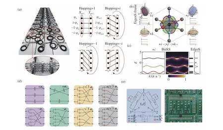
Fig.6 (a-c)Experimental observation of non-Abelian topological charges in a transmission line network with braiding connectivity[63].(d,e)Experimental demonstration of the Rashba-Dresselhaus spin-orbit interaction(SOI)in a passive electrical circuit with non-Abelian gauge fields[65].图6 (a-c)具有编织耦合的传输线网络中的非阿贝尔拓扑电荷的实验观测[63]。(d,e)具有非阿贝尔规范场效应的拓扑电路中的Rashba-Dresselhaus自旋-轨道耦合现象的实验验证[65]。
The research on the experimental realization of topological physics with non-Abelian potential is just in its infancy,due to the complex hopping requirement that poses great challenges for its implementation in cold atom and photonic systems.Electrical circuit provides an ideal experimental platform for studying non-Abelian topological systems using braiding structures,and thus allowing flexible combination of non-Abelian tunneling with spatialtemporal modulation, non-reciprocal coupling,PT symmetry and nonlinear effects to produce moreunconventional physicssuch as Majorana fermions[36-66]and anyons[67].
8 Nonlinear topological circuit
Most topological insulators/semimetals studied so far are limited to thelinear regime, due to the difficulties in the generation of sufficient nonlinearity in condensed matter and photonics.Fortunately,a wide range of choices of nonlinear circuit components(e.g.diodes, varactor diodes,Bipolar Junction Transistor) provides much easier realization of nonlinear topological systems in electrical circuits.
Hadad et al.reported the observation of self-induced topological protection in a nonlinear SSH model circuit[68],as shown in Figure 7a,in which one of the coupling capacitors in each unit cell wasreplaced by a pair of varactor diodes in the back-toback configuration.Asthecapacitance of the varactor diode decreases with the increasing of the voltage across it(Figure 7a), the circuit gains different level of nonlinearity at different level of input signals.They investigated the nonlinear dynamics of the circuit by analyzing the phase portrait,and found that the circuit entered the nontrivial state for large input signal,which was manifested as an even voltage distribution in both resonators of a unit cell with opposite phase.A sample having six unit cells was fabricated to confirm their theoretical predictions,which exhibited a self-induced topological edge state at large input signal(25 dBm),manifested as an obvious impedance peak at 98 MHz(Figure 7b),and was robust to circuit defects(mimicked by certain nodes short to ground).While for small input signals(0 dBm), the circuit was in the trivial state with multiple small impedance peaks that are susceptible to circuit defects.Based on the same nonlinear circuit array,the group also reported another work on the numerical simulations of self-induced solitons and propagating domain walls in a similar nonlinear circuit[69].
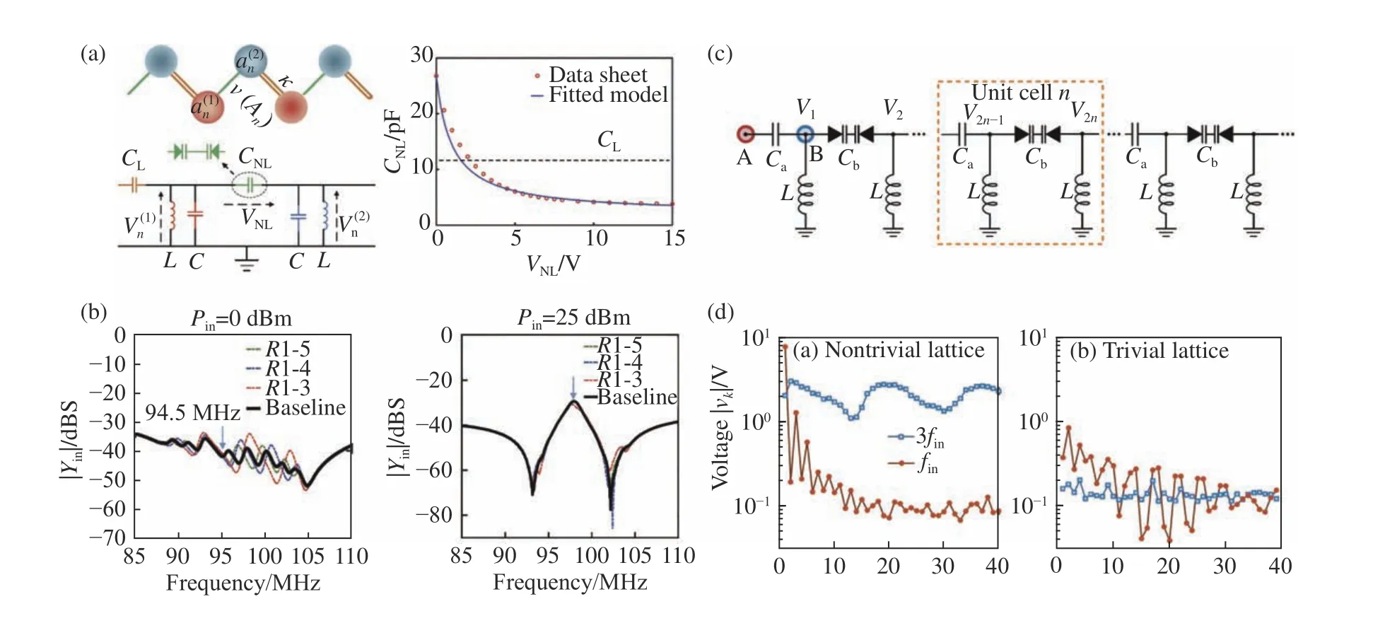
Fig.7 (a,b)Self-induced topological protection in a nonlinear SSH model circuit[68].(c,d)Topologically enhanced harmonic generation in a nonlinear circuit[70].图7 (a,b)非线性拓扑电路中的自感应拓扑保护[68]。(c,d)非线性电路中的拓扑增强的谐波产生[70]。
In 2019,Wang et al. presented topologically enhanced harmonic generation in a nonlinear circuit shown in Figure 7c[70].They found that the existence of topological edge state helped enhance the intensity of generated third-harmonic component by a factor of 250 as compared to the trivial case(Figure 7d).Such topologically enhanced nonlinear circuit may have applications in efficient and robust traveling-wave parametric amplification. Note that a variation of such nonlinear SSH circuits have been studied at an early time in 1970s by a group of scientists from Japan[71-75],in which a chain of varactor diodes was coupled with identical inductors.They called such circuit the Toda lattice,which supports soliton solutions to the Korteweg-de Vries (KDV)equation.
Due to the lack of efficient mathematical tool for analyzing the topology of nonlinear system and thedifficulties in detecting nonlinear state, the current study of nonlinear topological circuit is still limited to one dimension and in lack of a strict definition of the topological invariant.For the next stage, many exotic features of nonlinear effect including chaos,solitons,fractals can be expected to be introduced to topological circuit to induce new physics.
9 Conclusion
Here, we summarize some major advantages of topological circuits.Electrical circuits with flexible circuit connections and a wide choice of circuit devices provide a convenient and low-cost test bed for exploring many new topological models. The arbitrary connections among circuit nodes at arbitrary distances endow the circuits with unique properties of non-locality and higher dimensionality,giving access to genuine higher-dimensional topological systems,and all-bulk systems(with boundaries connected)possessing non-trivial manifolds such as Mobiüs strips and Klein bottles,complex nodal lines and nodal links with arbitrary linkageand knot topology in 3D/4D momentum space.Besides,electrical circuits allow us to probe into the bulk nodes and thus enabling recovering the entire band structure in experiment,which is impossible for rigid materials in condensed matter and photonics. Note that advanced data fitting algorithm or machine learning technique should be employed to assist the reconstruction of the circuit band structure[76], because it is not practically possible to experimentally measure theN-by-Ncircuit Laplacian of the entire circuit havingNcircuit nodes.
Topological circuitsarecurrently advancing toward non-Hermitian,higher-dimensional with higher-order topological states and peculiar knot topologies.A few representative works include the observation of corner state in a 4D circuit protected by hexadecapole moment[77],realization of nodal knots in circuits with mirror-image partners[76],exploration of reciprocal skin effect in a passive RLC circuit[78].Owing to the unique advantages of engineering long-range hopping and sufficient nonlinearity in circuit,topological circuits are becoming increasingly popular as a perfect platform for emulating non-Abelian band theory and nonlinear topological physics,and also a cost-effective platform for teaching topological materials.
Acknowledgements
This work wasfunded by the European Union’s Horizon 2020 Research and Innovation Programme under the Marie Sklodowska-Curie Grant Agreement No 833797, the Royal Society, the Wolfson Foundation,Horizon 2020 Action Project No.734578(D-SPA)and 648783(TOPOLOGICAL),the National Key Research and Development Program of China (Grant No.2017YFA0700201,2017YFA0700202,2017YFA0700203),the National Natural Science Foundation of China (Grant Nos.61631007,61571117,61875133,11874269),and in part by the111 Project (GrantNo.111-2-05).
