Passivation of PEA+to MAPbI3(110)surface states by first-principles calculations∗
2021-05-06WeiHu胡伟YingTian田颖HongTaoXue薛红涛WenShengLi李文生andFuLingTang汤富领
Wei Hu(胡伟), Ying Tian(田颖), Hong-Tao Xue(薛红涛),Wen-Sheng Li(李文生), and Fu-Ling Tang(汤富领),†
1School of Materials Science and Engineering,Lanzhou University of Technology,Lanzhou 730050,China
2State Key Laboratory of Advanced Processing and Recycling of Nonferrous Metals,Lanzhou University of Technology,Lanzhou 730050,China
3Department of Materials Engineering,Lanzhou Institute of Technology,Lanzhou 730050,China
Keywords: first-principles calculations,surface states,passivation
1. Introduction
Although the photoelectric conversion efficiency (PCE)has increased rapidly since the advent of perovskite solar cells(PSCs), researchers are still facing many challenges, such as preparing large-area perovskite films,[1]improving the oxidation stability of the device,[2]and developing effective technology to passivate the surface/interface defects.[3]Besides the properties of each layer material, the surface/interface structures and properties of solar cells are also crucial to the performance, which has led to a recent research focus in pursuing higher conversion efficiency.[4–9]For PSCs,defects of the bulk phase, the grain boundary, and the surface or interface will significantly affect carrier transport and charge recombination, which hinders improving the efficiency of PSCs. In addition,the battery materials prepared under mild conditions are far from the equilibrium state. Thus, there are rich interfaces,structural disorders and defects,which can lead to lower reproducibility of experiments and poor device stability.[10]For this reason,developers try to improve battery performance by modifying and adjusting the surface or interface. Surface states are one of the reasons for low conversion efficiency and poor stability of devices.Therefore,optimizing the passivation method is also a primary way to improve the efficiency and stability of the device. Below, we briefly review some experimental results of perovskite solar cell interface research and regulation. In 2019,You et al. summarized the latest progress of effective defect passivation about perovskite solar cells and described in detail the passivation methods of traditional solar cells.[11]For example, two-dimensional perovskite,[12,13]halogen ion,[14]and other materials with wide band gap[15]are commonly used to passivate surface defects. Moreover,the national renewable energy laboratory (NREL) also introduced the necessity of passivation of bulk or surface (interface) defects by additives and summarized the performances of additives used to control surface defects of perovskite,such as metal cations, fullerene derivatives, ammonium salts, low dimensional perovskite.[16,17]Abdi-Jalebi et al. found that when KI was added to the perovskite precursor, K+would accumulate on the surface to passivate those expanding defects; thus, the perovskite film with PCE of 21.5% could be produced.[18]Lee et al. reported the advantages of adding PEA+into 3D perovskite, and the wide band gap quasi-2D perovskite based on PEA+is conducive to reducing the defect density and slowing down the degradation of the unpacked devices.[19]Compared with the traditional 3D perovskite, the low-dimensional perovskite with 2D layered structure has better phase stability due to its large organic cation; in addition, the hydrophobic effect of phenyl makes the device have better moisture resistance.[20,21]Among low-dimensional perovskites,the passivation effect of phenethylammonium iodide(PEAI)is most commendable,[22–24]probably due to the more ordered 2D passivation layer formed by PEAI, and the synergistic effect of three groups is conducive to the longitudinal transport.[25]Based on this, the first principle calculation method based on density functional theory is used to study the passivation effect of PEA+on the electronic states of MAPbI3(110)surface.
2. Methods and model
In this work, all the calculations are performed with the code package VASP based on the density functional theory (DFT).[26,27]The exchange–correlation energy is described by the functional of Perdew–Burke–Ernzerh (PBE)[28]in the generalized gradient approximation (GGA), and the pseudopotential is described by projector-augmented wave(PAW).[29]By cutting the bulk MAPbI3along the(110)direction, when surface termination is MA+cation (as shown in Fig.1),the system contains 6 periodic atomic layers(excluding pseudo-H layer)of A-B,and the structure of the model is complete.In order to make the PEA+cations play an effective passivation role on this surface,I is made the surface terminal atom,and the top A-layer1 is deleted.The model forms a symmetrical nonpolar surface of the upper and lower atomic layers. PEA+is placed on the exposed and clean MAPbI3(110)surface with B-layer2 to establish the adsorption model. The passivation of H atom is added to eliminate the influence of the surface hanging bond of the bottom atom. The adsorption system consists of 84 atoms(43 H,6 N,13 C,17 I,and 5 Pb).The electronic configurations of Pb,I,N,C and H atoms in the crystal model are[Xe]5d106s26p2,[Kr]4d105s25p5,C 2s22p2,N 2s22p3and 1s1,respectively. The cutoff energy of MAPbI3surface and its adsorption system is 520 eV, and the k-point grids of the Brillouin region are set to 6×4×1. We use the conjugate gradient algorithm to optimize the original structure of the clean surface and the adsorption model. The convergence condition of the atomic force is set to 5×10⁻²eV/˚A.Then, the adsorption energy and density of states (DOS) of the model are calculated according to the Bloch tetrahedron method.
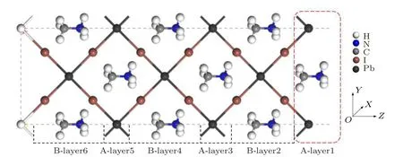
Fig.1. Atomic terminal of MAPbI3 (110)surface model.
3. Results and discussion
3.1. Lattice structure and electronic properties of clean MAPbI3 (110)surface

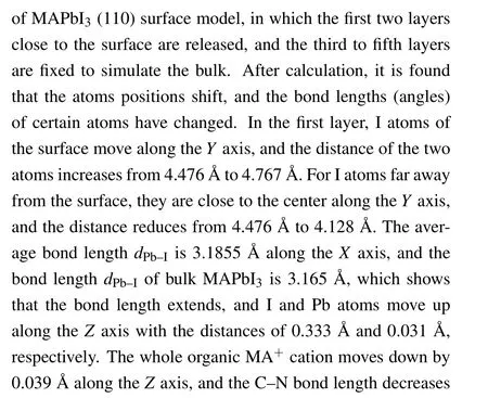
Figure 3 shows the total density of states (TDOS) of clean MAPbI3(110) surface, and the local density of states(LDOS)of each layer,and the partial density of states(PDOS)of some atoms on the surface. From the TDOS (Fig.3(a)),it can be found that there is a peak near the Fermi level between −1 eV and −0.5 eV, and DOS is 11.5 at the Fermi level, which indicates the existence of electronic states. According to Figs.3(b)–3(f),it can be found that these electronic states mainly come from the first,the third,and the fifth layer of atoms. From Figs. 3(g)–3(j), the peak of density of states is mainly contributed by the I-5p, Pb-6s, and Pb-6p orbitals on the first layer of the surface near the Fermi level. These electronic states are surface states, which may have harmful effects on the surface. The main reason is that the existence of the electronic states leads to the radiation compound loss of the photo-generated carriers on the surface, which reduces the PCE of devices. Therefore, it is particularly important to find the surface passivators to weaken or even eliminate the electronic states.
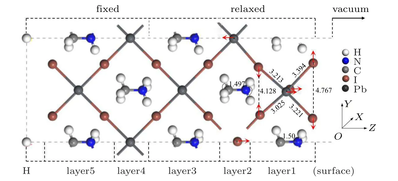
Fig.2. The optimized atomic position change of clean MAPbI3 (110)surface.
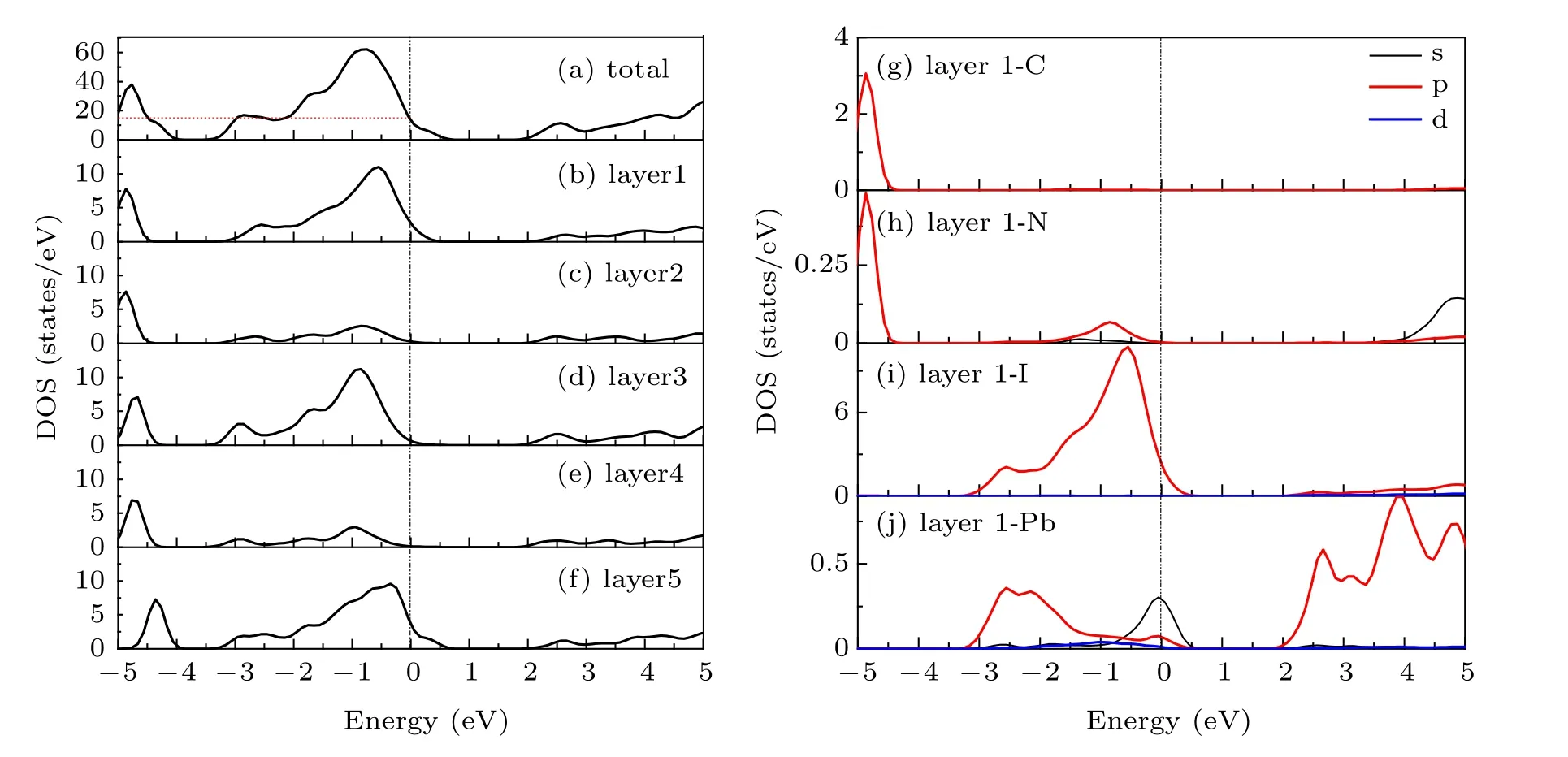
Fig.3. (a)The TDOS of clean MAPbI3 (110)surface;(b)–(f)the LDOS of layer1–layer5;(g)–(j)the PDOS of layer1.
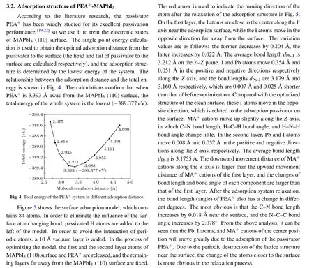
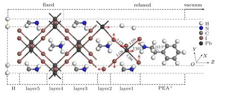
Fig.5. The change of atom position in the optimized adsorption system.
3.3. Adsorption energy and electronic properties of PEA+-MAPbI3 adsorption system
The stability of surface adsorption is related to the adsorption energy of the system. In other words, if the adsorption energy is negative,the smaller the value,the more stable the adsorption of molecules or atoms on the surface.[30]Equation(1)is used to calculate the adsorption energy of PEA+on MAPbI3(110)surface[31]Eatom/MAPbI3and EMAPbI3represent the total energy of adsorption system and clean surface MAPbI3(110),respectively.Eatomis the total energy of the adsorbate PEA+. N is 1,which means to adsorb a molecule.The adsorption energy of the system is −3.898 eV.The result shows that the system has higher absorbability, and it also shows that the passivator has good stability on this surface.
Surface states (electronic states) are an unfavorable factor for solar cells. It serves as a carrier recombination center for photogenerated carriers and will thereby reduce the carrier lifetime as well as PCE.Compared Fig.3 with Fig.6,the passivation effect of PEA+on the MAPbI3(110) surface can be analyzed. It can be seen that the passivator PEA+greatly reduces the electronic states of MAPbI3surface,and its value of total DOS decreases from 11.5 to 6.5 at the Fermi level. Thus,PEA+treatment should greatly suppress trap-assisted charge recombination and improve PCE. This is basically consistent with the experimental results of Zhang et al.[22–24]Through the analysis of the PDOS,it may be seen that the decrease of the electronic states peak value is mainly due to the contribution of I-5p and Pb-6p, Pb-6s on the first layer of MAPbI3(110) surface near the Fermi level within −1.5 to 0.3 eV.Moreover,compared with the band gap of clean MAPbI3(110)surface, the band gap of the adsorption system decreases significantly, and it also shows that PEA+can regulate the band gap of MAPbI3(110)surface. Figure 6(b)shows that the adsorption of PEA+does not introduce new electronic states,which has a good passivation effect. Compared with the local density of states of clean MAPbI3(110)surfaces(Figs.5(b)–5(e)),it can be seen that the first four layers have no DOS peak due to the addition of passivator near the Fermi level.In particular,the passivation effect of PEA+on the first and third layers is most obvious in Figs.6(c)–6(f). Figures 6(i)–6(n)show the PDOS of C, N, I, and Pb atoms at the adsorption surfaces of MAPbI3/PEA+. According to Figs.6(i),6(l)and 6(n),there is hybridization of C-2p orbital of PEA+and N-2s with the Pb-6p orbital of MAPbI3near the Fermi level within 1.5 to 2.5 eV.Figures 6(i)and 6(m)show that there is a hybridization of C-2p orbital of PEA+and I-5p orbital of MAPbI3. According to the above analysis,the adsorption of PEA+on the MAPbI3(110)surface has a good passivation effect,and the electronic orbital hybridization also promotes interaction between atoms.
Charge density difference and Bader charge are qualitative and quantitatively described of the surface charge transfer degree,respectively. By calculating the charge density difference and Bader charge, we can fully understand the charge transfer of the whole system.[32]Charge density difference is calculated by

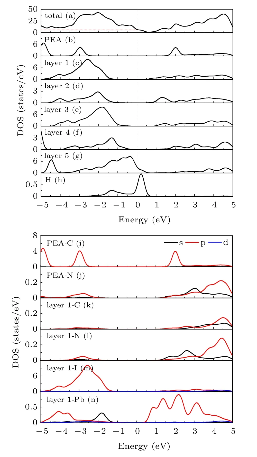
Fig.6. (a)The TDOS of PEA+-MAPbI3 adsorption system;(b)the LDOS of PEA+;(c)–(g)the LDOS of layer1–layer5;(h)the LDOS of passivation H;(i)–(n)the PDOS of PEA+ and MAPbI3 (110)layer1.
Figure 7 shows the charge density difference of PEA+adsorbed on the surface of MAPbI3(110). The increase(positive) or decrease (negative) of charge density is indicated by yellow and cyan,respectively.Figure 7(a)is the charge density difference of the adsorption system,and Fig.7(b)is a partially enlarged diagram of the charge density difference of the adsorption system. From Fig.7(a),it can be seen that the charge transfer takes place throughout the system but mainly concentrates near the surface;the farther from the surface,the smaller the charge transfer. The charge density difference culminates on the surface, and the charge transfers are directed to both sides of the surface,which will promote the bonding strength between the surface atoms,leading to strong atoms interaction on the surface. From Fig.7(b),it can be seen that I atoms gain electrons,and Pb atoms lose electrons. For the PEA+part,the number of C atoms electron is reduced while the number of N atom electron increases near the surface.
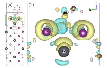
Fig.7. Density charge difference of the PEA+-MAPbI3 adsorption system.
The amount of charge transfer is analyzed by calculating the Bader charge of each atom of the adsorption structure surface and bulk phase. Table 1 shows the Bader charges of I,Pb,C,N atoms of MAPbI3and PEA+bulk,and that of the adsorption system near the surface. It can be found that I5,I11,and I17 atoms get 0.588e,0.669e,and 0.684e,respectively,while Pb5 atom loses 0.892e on the first layer of adsorption system MAPbI3. Compared with the Bader charge of I and Pb atoms in the original phase, I and Pb atoms of the adsorption system gain or lose more electrons. Compared Bader charge of the adsorption system PEA+with that of the independent system PEA+,it can be seen that N atom gets 2.944e,C12 atom gets 0.779e,and C13 loses 0.523e near the adsorption system surface.To sum up,through the analysis of Figs.6 and 7,combined with Bader charge,it can be seen that the decrease of the surface states of MAPbI3(110)is mainly due to the contribution of C and N atoms of passivator PEA+. The above results show that the Bader charge changes greatly before and after PEA+adsorbed on the MAPbI3surface, which indicates that the surface chemical reaction is strong. On the other hand, it can be seen that the farther away from the surface,the smaller the charge transfer.
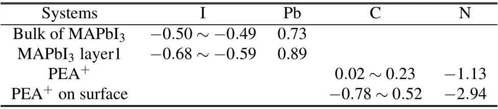
Table 1. Bader charges of some atoms of MAPbI3 bulk and PEA+-MAPbI3 adsorption system.
4. Conclusion
In this work, the passivation effect of PEA+to the electronic states of MAPbI3(110) surface is studied using VASP software based on the first principle calculations. The results show that surface electrons are redistributed and the surface states are passivated. The C and N atoms of the passivator PEA+surface can eliminate the surface states,which is mainly due to the contribution of I-5p and Pb-6p,Pb-6s on the first and the third layer of MAPbI3(110) surface near the Fermi level between −1.5 eV and 0.3 eV by adding the passivator. The study of passivated surface provides a theoretical guideline for enhancing the transmission of photogenerated carriers and is inspiring to improve the PCE of MAPbI3-based solar cells.
Acknowledgment
This work was performed in the Gansu Supercomputer Center.
猜你喜欢
杂志排行
Chinese Physics B的其它文章
- Quantum annealing for semi-supervised learning
- Taking tomographic measurements for photonic qubits 88 ns before they are created*
- First principles study of behavior of helium at Fe(110)–graphene interface∗
- Instability of single-walled carbon nanotubes conveying Jeffrey fluid∗
- Relationship between manifold smoothness and adversarial vulnerability in deep learning with local errors∗
- Weak-focused acoustic vortex generated by a focused ring array of planar transducers and its application in large-scale rotational object manipulation∗