Quantization of the band at the surface of charge density wave material 2H-TaSe2∗
2021-05-06ManLi李满NanXu徐楠JianfengZhang张建丰RuiLou娄睿MingShi史明LijunLi黎丽君HechangLei雷和畅CedomirPetrovicZhonghaoLiu刘中灏KaiLiu刘凯YaoboHuang黄耀波andShancaiWang王善才
Man Li(李满), Nan Xu(徐楠), Jianfeng Zhang(张建丰), Rui Lou(娄睿),Ming Shi(史明), Lijun Li(黎丽君), Hechang Lei(雷和畅), Cedomir Petrovic,Zhonghao Liu(刘中灏), Kai Liu(刘凯), Yaobo Huang(黄耀波), and Shancai Wang(王善才),§
1Department of Physics and Beijing Key Laboratory of Opto-electronic Functional Materials&Micro-nano Devices,Renmin University of China,Beijing 100872,China
2Shanghai Synchrotron Radiation Facility,Shanghai Institute of Applied Physics,Chinese Academy of Sciences,Shanghai 201204,China
3Institute of Advanced Studies,Wuhan University,Wuhan 430072,China
4Swiss Light Source,Paul Scherrer Institute,CH-5232 Villigen,Switzerland
5Chongqing Technology and Busineee University,Chongqing 400067,China
6Condensed Matter Physics and Materials Science Department,Brookhaven National Laboratory,Upton,NY 11973,USA
7State Key Laboratory of Functional Materials for Informatics and Center for Excellence in Superconducting Electronics,SIMIT,Chinese Academy of Sciences,Shanghai 200050,China
Keywords: angle-resolved photoemission spectroscopy,transition metal dichalcogenide,TaSe2
1. Introduction
Manipulation of two-dimensional electron gas (2DEGS)has recently drawn considerable interest.[1–4]As a mechanism for tailoring the many-body interactions, 2DEGS is embodied in the interface of semiconductors[5–7]and metalfilms.[8–10]This has attracted a lot of interests due to observation of high electron mobility,[11,12]quantum Hall effect,[13,14]superconductivity,[15]large magnetoresistance,[16]etc. The 2DEGS is generally caused by the confinement of electrons along one dimension,for example,by the depletion of charge carriers close to the surface and then inducing a band-bending to confine the electrons into 2DEGS.[17]Due to the shielding effect of good conductors, it is difficult to achieve 2DEG in metals. Monolayer transition metal dichalcogenides (TMDs)MX2(M = Mo, W; X = S, Se) represent a natural host for 2DEGS.[18]
The mechanism of CDW in quasi-two-dimensional TMDs is a controversial topic for a few decades. Both weak-coupling approaches and strong coupling mean-field models have been proposed, e.g., the Fermi surface (FS)nesting,[19–21]saddle point,[22–24]local chemical bonds,[25,26]excitonic insulator,[27–29]and lattice-driven models,[30–32]however, no consensus has been reached in the driving mechanism of the CDW in TMDs. On the other hand,there is coexistence/competition between the CDW and superconductivity[33,34]in many TMDs. Thus the understanding of the CDW mechanism remains a challenge.
The 2H-TaSe2consists of three-atom-thick chalcogentransition metal-chalcogen sandwiches and its unit cell can be considered as two layers of Ta-Se with a 60◦rotation with van der Waals’force in adjoining layers.[33]2H-TaSe2undergoes a second-order transition from normal phase to an incommensurate ordered phase at T=122 K,followed by a first-order lockin transition to a 3×3 commensurate CDW (CCDW) phase at TCDW= 90 K.[33,35]The CDW mechanism in 2H-TaSe2has been investigated experimentally by ARPES,STM,transport measurement, neutron scattering,[20,21,35–44]and band structure calculations.[45–47]Recently, the k-dependence of susceptibility and k-integrated function calculations disagree with the CDW wave vectors in 2H-TaSe2and the FS nesting scenario is excluded as a driven force.[32,45,48]The strong electron–phonon coupling with wave-vector-dependent electron–phonon matrix elements[30,32]and a new type of collective excitation[37]as the condensation of preformed excitons[49]are proposed,but further evidence is needed.
In this paper, we report an ARPES study of the electronic structure of 2H-TaSe2with various photon energies in the compensate CDW state and normal state. In addition to the 2D-like band structure reported before, we report a quantized state induced by the intrinsic band structure at Brillouin zone center (Γ) below EFin 2H-TaSe2single crystal for the first time. It is formed by a band with strong kzdispersion and approaches EFnear 3D BZ center predicted in the bulk band calculation, but not reported in the ARPES measurement before. The combination of near-surface band-bending potential created by the rearrangement of surface electrons and the light effective mass along kzdirection causes the quantization along c-axis and the formation of the manifold sub-bands at the surface, similar to that in semiconductors.[17]With the decrease of temperature below TCDW,the sub-bands shift upward while most of the bulk bands show no noticeable change. This abnormal band shift may be related to the CDW but could not be explained yet. When neither the model of Fermi surface nesting nor the electron–phonon coupling could successfully explain the origin of CDW in 2H-TaSe2,our discovery and extensive analysis of those results may unlock new perspectives and avenues for understanding the CDW mechanism.

2. Materials and methods
Single crystals of 2H-TaSe2were grown by the iodine vapor transport method. The element analysis and transport measurement of the samples indicate the high quality of crystals in this paper.[33]ARPES measurement was performed at the Dreamline beamline of the Shanghai Synchrotron Radiation Facility with a Scienta D80 analyzer and at the SISHRPES beamline of the Swiss Light Source with a Scienta R4000 analyzer. The energy and angular resolutions were better than 15 meV and 0.2◦, respectively. The sample for the ARPES measurements was cleaved in situ along (001)direction in a vacuum better than 5×10⁻¹¹Torr. Normal and CDW phases measurements were taken at T = 150 K and T =20 K, respectively. The electronic structure of 2HTaSe2was studied by using first-principles calculations with the projector augmented wave (PAW) method[50,51]as implemented in the VASP package.[52–54]For the exchange–correlation functional,the generalized gradient approximation(GGA) of the Perdew–Burke–Ernzerhof (PBE) formula[55]was adopted.The kinetic energy cutoff of the plane-wave basis was set to be 300 eV.A 16×16×4 k-point mesh was utilized for the Brillouin zone (BZ) sampling and the Fermi surface was broadened by the Gaussian smearing method with a width of 0.05 eV. The vdW interactions between the TaSe2layers were considered by adopting the optB86b-vdW functional.[56]The lattice parameters and internal atomic positions were fully relaxed until the forces on all atoms were smaller than 0.01 V/˚A.After the equilibrium structures were obtained,the electronic structures were calculated by including the spin–orbit-coupling (SOC) effect. In the slab calculation, a twodimensional supercell with a 21-layer TaSe2slab and a 20-˚A vacuum was employed.
3. Results and discussion


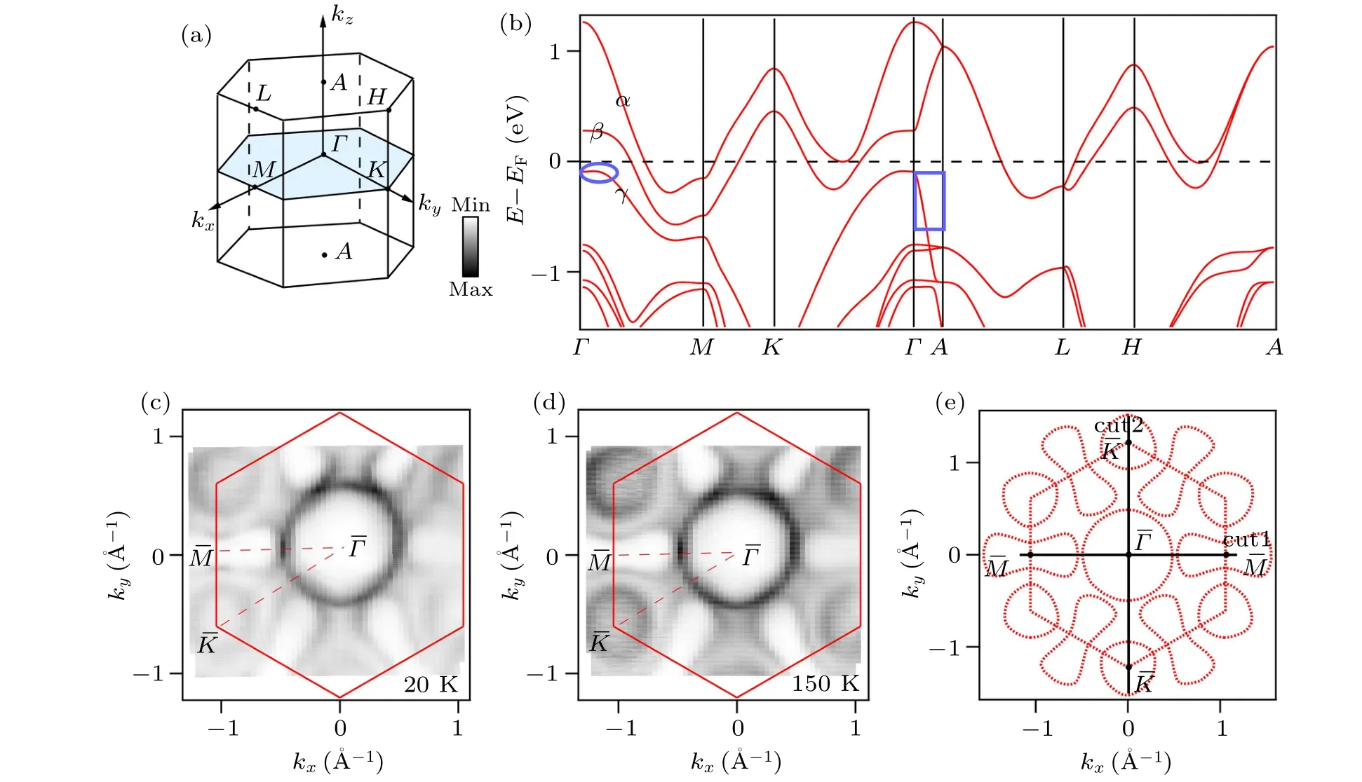
Fig.1. Brillouin zone and Fermi surface of 2H-TaSe2. (a)3D bulk BZ with marked high-symmetry points and a colored high symmetry plane.(b)Calculated bulk band structure along high-symmetry lines including SOC.Three near-EF bands are denoted as α, β, and γ, respectively.(c),(d)Integrated intensity plots within EF±10 meV at T =20 K and 150 K to show the FS topology,obtained with hν =50 eV showing the colored plane indicated in(a),corresponding to CDW and normal phase,respectively. (e)The extracted ARPES mapping in the normal state.Marked cuts#1 and#2 indicate the momentum locations of the measured bands in Fig.3.


Fig.2. Temperature dependence of band gap. (a) The band dispersion along the direction of at T =10 K, ∆is the CDW gap. (b)Same as(a),but displayed at T =160 K.(c),(d)The temperature dependence of symmetrized EDCs along the momentum marked by#a and#b,respectively. (e)The extracted band gap(∆)as a function of temperature. (f)The gap varies with momentum position(θ)atpocket.

In order to study the band structure under the influence of surface band bending,we performed the band structure calculations with a 21-layer slab,and plot the results along with high symmetry lines in Figs.3(c)and 3(h). The slab calculation reproduces the sub-bands qualitatively in agreement with our experimental results. The separations of γ subbands are more pronounced than the other bands,in agreement with the observations. This larger separation is due to the lower effective mass along the quantization dimension(c-axis),which can be seen from the dispersion along Γ–A in the bulk band calculation.
To quantitatively study the relationship between the band structure close to the Fermi level and the CDW transition,we have traced the three bands,α,β,and γ as noted in bulk band calculation in Fig.(b),to view their changes with temperature.The measured CDW/normal state band dispersions are illustrated in Figs. 3(a)/3(d) and 3(f)/3(i), along ¯Γ– ¯M and ¯Γ–¯K,respectively. At the low temperature, in spite of the shadow bands caused by the 3×3 reconstruction and the opening of CDW gaps close to EF, the bands show no noticeable energy shift compared with the normal state. In contrast, the quantized γ sub-bands shift upward while the bulk band of Γ-certer shifts downward with the temperature decrease. The binding energy of the topmost sub-band shifts upward by about 30 meV,from EB∼485 meV at T=150 K to EB∼455 meV at T =20 K which is beyond the experimental resolution,and so are the following sub-bands. The bulk band of Γ-center shifts downward by about 20 meV,from EB∼0.92 eV at T =150 K to EB∼0.94 eV at T =20 K. In order to compare the energy shift of the bands, we overlay the EDCs at below and above TCDWat points marked as‘1’and‘2’in Figs.3(a)and 3(d),and show them in Figs.3(k)and 3(l),respectively. From Fig.3(k),no band shift is observed across the TCDWfor α and β bands within the energy resolution,while the quantized subbands of γ and bulk band at Γ-center show a clear shift with temperature changes.
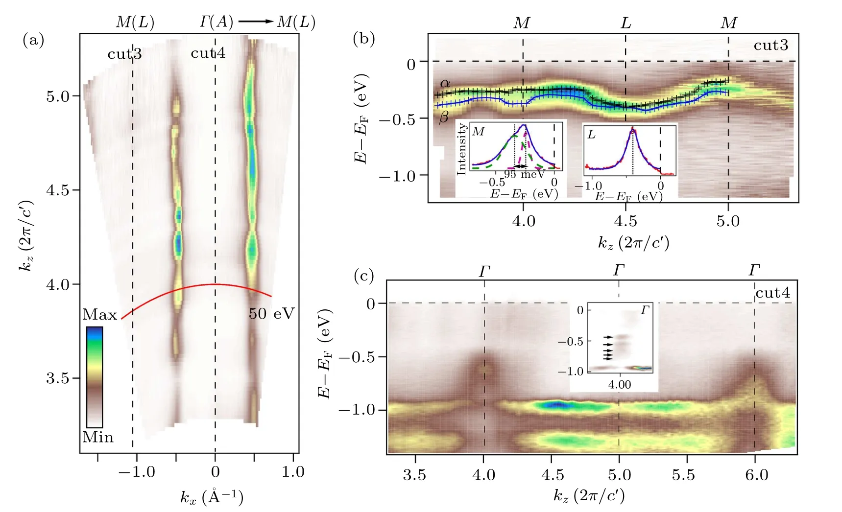
We further perform the kz-dependent measurements in Γ M–AL plane by varying the photon energy, covering more than one BZ along kz. Figure 4(a)shows the integrated spectra intensity plot around EFas a function of kxand kz,defined as cut#1 in Fig.1(e). The α,β bands are nearly degenerate and show little dispersion along kz, confirming the 2D like characters of the bands. We also show the band dispersion along M–L and Γ–A,labeled as cut#3 and cut#4,in Figs.4(b)and 4(c),respectively. The kzvalue is converted with the inner potential V0=17 eV empirically to best fit the dispersion. Figure 4(b)shows the ARPES intensity plot along the M–L line,a clear dispersion along kzat BZ boundary confirms the periodic variation of electronic states. The insets show EDCs at high symmetry points (i.e., M and L), where α and β bands split at M and nearly degenerate at L, in agreement with the bulk band calculation shown in Fig.1(b).

Fig.4. Photon-energy-dependent band dispersion of 2H-TaSe2. (a)Integrated ARPES intensity map within EF±10 meV in the hν–khplane,where khis oriented along the Γ–M(A–L)direction,recorded with various photon energies. (b)ARPES intensity plot along the M–L direction,from cut#3 in Fig.4(a),the markers are guided to the eyes. Insets show multiple Gaussian peaks fit the EDCs at high symmetry points M and L, respectively. (c)ARPES intensity plot along the Γ–A direction, cut #4, taken with photon energies covering a kz range over 2 BZs. Inset shows a zoom-in second derivative plot at Γ point.

It has been a long-standing puzzle that the γ band is absent and only two hole-like bands in the BZ center are observed.For a band with fast dispersion and light effective mass along the c-axis, the band bending effect, which is caused by the breaking of translation symmetry at the surface,will make the quantization more observable and hinder the observation of the bulk band.From the bulk band calculation(Fig.1(b)),the γ band disperses rapidly along Γ–A,with relatively flat in-plane dispersion. As aforementioned slab calculation,the quantized states are located at higher binding energies than the bulk band calculation. In contrast,the quantization of α,β bands is not as clear as that of γ band due to slower dispersion and higher effective mass along the c-axis. This can be seen from the less separation of the states in the slab calculations. From the comparison between the bulk band and the slab calculations,in addition to the consistency between ARPES measurement and slab calculation,we safely“recover”a missing bulk band in 2H-TaSe2in the vicinity of EFcentered at 3D BZ center,with fast dispersion along kz.

Based on the observation of the quantized states, and the DFT and slab calculations, we “recover” the bulk γ band with band top near EFand a relatively flat in-plane dispersion around the 3D BZ center. Since the quantized states respond with the CDW transition,they could participate in or influence by the formation of CDW. As a surface-sensitive measurement, ARPES observation of the bulk Γ band is hindered by the quantization,and we can only observe the quantized states at the top few layers. In order to confirm if the shift is a CDW related bulk band character or a chemical-shift of the quantized surface state, bulk sensitive measurement such as x-ray ARPES is needed. The band shift of γ band with temperature is inconsistent with the FS nesting,electron–phonon coupling,or preformed exciton liquid scenario.[29,57,59]The understanding of the shift with temperature remains a challenge at the moment, it may cast new perspectives in understanding the CDW mechanism. We expect further bulk sensitive measurement and a better theoretical explanation for this phenomenon in the future.
4. Summary
In conclusion, we measured the band structure of 2HTaSe2and measured the temperature and angular dependence of the CDW gap variation. We have observed quantized states in single crystal 2H-TaSe2for the first time. We studied the in-plane and kzdependence of the band dispersion and found out the quantization from a previous “missing” band, which is close to Fermi energy in Γ–M–K plane and highly dispersive along kz. That quantization at the surface results from the band bending due to the surface electron rearrangement and the light carriers’effective mass of the band along Γ–A direction. The band shifts upward with the decrease of temperature into the CCDW state, and the unusual shift is mostly related to the CDW transition. Further bulk sensitive measurement of γ band is needed and it may pave an avenue to understand the CDW in 2H-TMD materials.
Acknowledgements
The authors thank Qiang Han for valuable discussions.Y. H. was supported by the CAS Pioneer Hundred Talents Program (type C). Work at Brookhaven National Laboratory was supported by US DOE, Office of Science, Office of Basic Energy Sciences (DOEBES), under Contract No. DESC0012704(materials synthesis).
猜你喜欢
杂志排行
Chinese Physics B的其它文章
- Quantum annealing for semi-supervised learning
- Taking tomographic measurements for photonic qubits 88 ns before they are created*
- First principles study of behavior of helium at Fe(110)–graphene interface∗
- Instability of single-walled carbon nanotubes conveying Jeffrey fluid∗
- Relationship between manifold smoothness and adversarial vulnerability in deep learning with local errors∗
- Weak-focused acoustic vortex generated by a focused ring array of planar transducers and its application in large-scale rotational object manipulation∗
