1064 nm InGaAsP multi-junction laser power converters
2020-06-18JiajingYinYurunSunShuzhenYuYongmingZhaoRongweiLiandJianrongDong
Jiajing Yin , Yurun Sun Shuzhen Yu Yongming Zhao Rongwei Li and Jianrong Dong
1Key Laboratory of Nano Devices and Applications, Suzhou Institute of Nano-Tech and Nano-Bionics, Chinese Academy of Sciences,Suzhou 215123, China
2Nano Science and Technology Institute, University of Science and Technology of China, Hefei 230026, China
Abstract: Laser photovoltaic devices converting 1064 nm light energy into electric energy present a promising prospect in wireless energy transmission due to the commercial availability of high power 1064 nm lasers with very small divergence. Besides their high conversion efficiency, a high output voltage is also expected in a laser energy transmission system. Meanwhile,1064 nm InGaAsP multi-junction laser power converters have been developed using p+-InGaAs/n+-InGaAs tunnel junctions to connect sub-cells in series to obtain a high output voltage. The triple-junction laser power converter structures are grown on p-type InP substrates by metal-organic chemical vapor deposition (MOCVD), and InGaAsP laser power converters are fabricated by conventional photovoltaic device processing. The room-temperature I-V measurements show that the 1 × 1 cm2 triplejunction InGaAsP laser power converters demonstrate a conversion efficiency of 32.6% at a power density of 1.1 W/cm2, with an open-circuit voltage of 2.16 V and a fill factor of 0.74. In this paper, the characteristics of the laser power converters are analyzed and ways to improve the conversion efficiency are discussed.
Key words: InGaAsP; multi-junction laser power converter; conversion efficiency
1. Introduction
The open circuit voltage of a single-junction 1064 nm LPC is some 0.6-0.7 V, while several volts are usually required for power supplies in electronic systems. To make the LPCs practically useful for real situations, two schemes could be used to increase output voltage: the first is to connect multiple single-junction LPCs placed side-by-side in series[16−18]and the second is to vertically stack sub-cells connected by tunnel junctions to form multi-junction LPCs[19−23]. In this paper, vertically-stacked triple-junction InGaAsP LPCs for converting the power of a 1064 nm laser are developed. So far, there have been no reports on multi-junction 1064 nm LPCs.
The structures of InGaAsP triple-junction LPCs were grown by MOCVD, and LPCs with an aperture of 1 × 1 cm2were fabricated. A conversion efficiency of 32.6% was achieved at a power density of 1.1 W/cm2under 1064 nm laser irradiation at room temperature with an open-circuit voltage of 2.16 V and a fill factor of 0.74.
2. Theoretical and experimental details
2.1. Structure design and calculation of I-V characteristics of triple-junction InGaAsP LPC
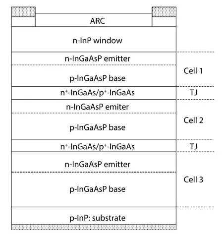
Fig. 1. Schematic layer structure of the designed triple-junction In-GaAsP LPC.
The absorbing layer thicknesses of each sub-cell of the triple-junction InGaAsP LPCs are designed based on the rule of current matching and the absorption coefficient of In-GaAsP material at 1064 nm. The thicknesses of the sub-cells can be determined using the following equation:
whereαis the absorption coefficient,xnis the thickness of the absorbing layer of thenth sub-cell from the top,fis the percentage of the light being absorbed by the LPC,Nis the number of the sub-cells. The ideal tunnel junction (TJ) connecting the sub-cells is transparent for the incident light.However, achieving both n-type and p-type doping concentration of more than 1 × 1019cm-3for InP and Al0.48In0.52As are difficult. Therefore, InGaAs is chosen to build the tunnel junctions for the triple-junction InGaAsP LPC. The depletion layer thickness of InGaAs TJ with a doping concentration of 1 ×1019cm-3on both sides is about 16 nm, and the thicknesses on two sides of the InGaAs pn junction are set to 20 nm considering the possible Zn diffusion. Fig. 1 shows the schematic structure of a vertically-stacked triple-junction InGaAsP LPC. Using 1.08 eV InGaAsP lattice matched to InP substrate as the absorption layer to obtain as high as possible voltage,while maintaining reasonable absorption coefficient at 1064 nm, the layer thicknesses of the triple-junction 1064 nm LPC are calculated to be 264, 456, and 2109 nm for cell 1, 2,and 3, respectively, based on the absorption coefficient of 1.4 × 104cm-1at 1064 nm for 1.08 eV InGaAsP[24]and taking into account of the absorption of incident 1064 nm light by the InGaAs tunnel junctions.
The current-voltage (I-V) characteristic of the LPC was calculated and the loss mechanisms (e.g., series resistance, reflection of surface, and surface recombination) were taken into consideration during the calculation. TheI-Vcharacteristic of the multi-junction InGaAsP LPC can be described by the following equation:
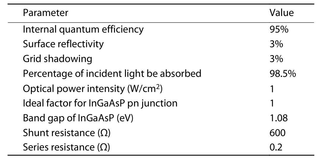
Table 1. Parameters for efficiency estimation of triple-junction In-GaAsP laser power converter.
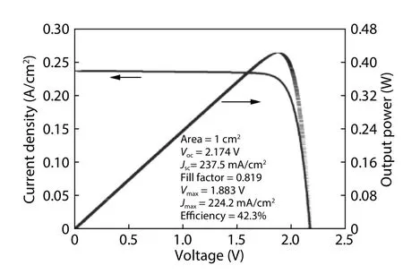
Fig. 2. Calculated I-V and P-V characteristics of the designed triple-junction InGaAsP LPC.
whereIis the output current,Iphthe photogenerated current of sub-cell,Isthe reverse saturation current,qthe electron charge,Vthe output voltage,kthe Boltzmann’s constant,Tthe temperature,nthe ideality factor of the diode,Nthe number of sub-cells,Rsthe series resistance, andRshthe shunt resistance of the sub-cell.
Table 1 shows the parameters used for the calculation of the characteristics of the triple-junction InGaAsP LPCs with an aperture of 1 × 1 cm2.
Fig. 2 shows calculatedI-VandP-Vcharacteristics of the triple-junction InGaAsP LPC at an incident 1064 nm laser power density of 1 W/cm2taking the absorption of the tunnel junctions into account, the short circuit current is 237.5 mA/cm2, the open circuit voltage is 2.174 V, the fill factor is 81.9%, and the conversion efficiency is 42.3%.
2.2. Material growth and device processing
Prior to the growth of the triple-junction InGaAsP LPC structures, InGaAsP epitaxial layers were grown to calibrate the composition and growth rate. Room temperature photoluminescence (PL) peak at 1153 nm confirms the band gap of InGaAsP of 1.08 eV.
I do, she said, touching9 the sleeve of my blouse. Today your son walked straight over to that child. I watched him hand her some pretty pink flowers and whisper, I love you.
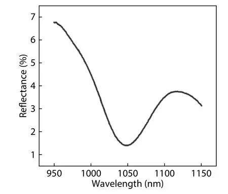
Fig. 3. Surface reflectance spectrum of the triple-junction InGaAsP LPCs with an antireflection coating.
The triple-junction LPC epitaxial structure was grown on p-type InP substrates by an AIXTRON-200/4 MOCVD system using trimethylgallium (TMGa) and trimethylindium (TMIn), as well as arsine (AsH3) and phosphine (PH3) as the group III and group V precursors, respectively, and ultra-high purity hydrogen (H2) as the carrier gas. Diethylzinc (DEZn) and silane(SiH4) were used as the p-type and n-type doping sources, respectively. Starting from the InP substrate, a 300-nm InP buffer with a Zn concentration of 2 × 1018cm−3was grown followed by InGaAsP sub-cells of 2310, 456, and 264 nm thick, respectively, separated by 20-nm n+-InGaAs (Si: 2 × 1019cm−3) /20-nm p+-InGaAs (Zn: 2 × 1019cm−3) tunnel junctions, and finally a 500-nm InP current spreading layer and a 100-nm In-GaAs contact layer with a Si concentration of 1 × 10¹⁸and 2 × 1019cm−3, respectively, were grown to finish the whole LPC structure. Each pn junction subcell comprised of a p-type and n-type layer doped with Zn and Si to 4 × 10¹⁷and 2 ×1018cm−3, respectively, and was sandwiched between a 50-nm InP back field layer doped with Zn of 2 × 1018cm−3and a 50-nm InP window layer doped with Si of 2 × 1018cm−3.
Triple-junction InGaAsP LPC was fabricated by evaporating front grid and back ohmic contact metals, etching of InGaAs contact layer, and finally depositing 85-nm SiO2/100-nm TiO2antireflection dielectric films. The reflectivity of the antireflection coating was measured using a reference sample and shown in Fig. 3, which confirmed the low reflection of 1.8% at 1064 nm. Subsequently, the LPC wafers were sawn into chips of 1 × 1 cm2. Silver paste was applied between LPC chips and Cu-plated ceramic heat sinks to improve thermal conductivity during the measurements.
3. Results and discussion
The measurement of laser LPC conversion efficiency was performed at room temperature, and the fiber guided 1064 nm optical beam with a divergence of about 25° perpendicularly illuminated the LPC chip surface with the end of the fiber at a distance to the surface to ensure that the whole light spot is received by the aperture.I-Vcurves of the triplejunction InGaAsP LPC under different 1064 nm monochromatic power densities of 610, 989, 1100, and 1233 mW/cm2are shown in Fig. 4 and the extracted parameters are shown in Table 2.
It can be seen from the Table 2 that the conversion efficiency of 32.13% at the optical power density of 989 mW/cm2is much lower than the expected conversion efficiency of around 42.3% based on the design. A little bit higher conversion efficiency of 32.6% and higher open circuit voltage of 2.16 V are achieved at 1.1 W/cm2. The series resistance and shunt resistance are determined to be 0.22 and 43 Ω of the sub-cell, respectively, by fitting theI-Vcurve obtained at 1100 mW/cm2using Eq. (2). The low shunt resistance indicates a significant leakage, probably via surface states of the side walls of the cell, which are not passivated by deposition of dielectrics.
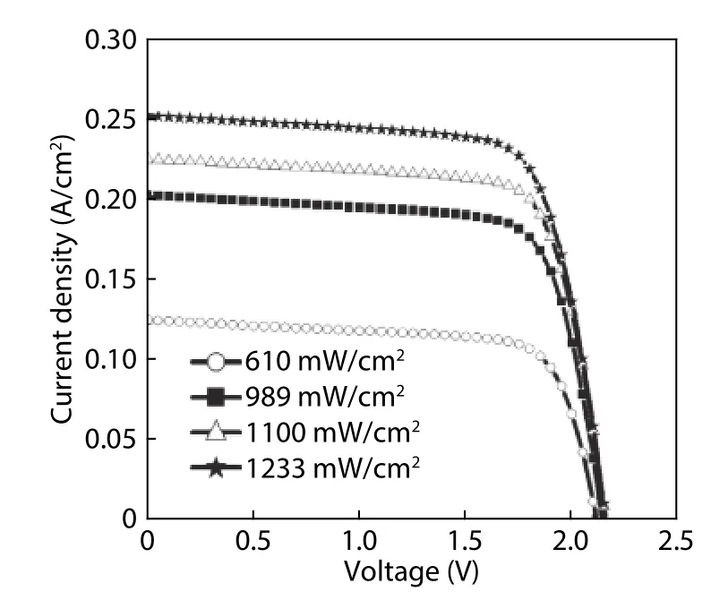
Fig. 4. I-V curves of a triple-junction InGaAsP LPC at different input 1064 nm laser power densities.
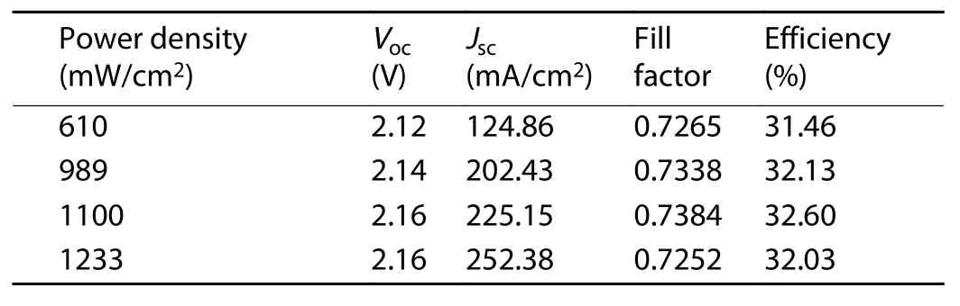
Table 2. Summary of the parameters of triple-junction InGaAsP LPC at laser power densities of 610, 989, 1100, and 1233 mW/cm2.
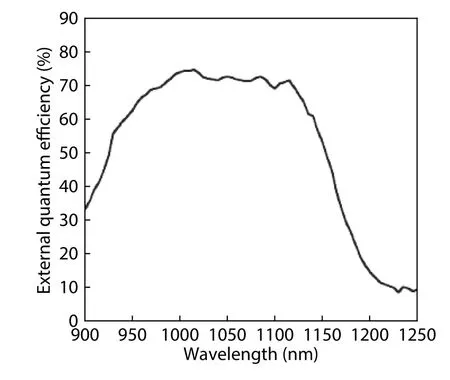
Fig. 5. External quantum efficiency of the triple-junction InGaAsP LPC.
To find the reasons why the conversion efficiency is lower than the expected efficiency, the external quantum efficiency (EQE) was measured using a xenon light source passing a monochromator and a standard Si cell as the reference. As shown in Fig. 5, the EQE at 1064 nm is 71.7% and is consistent with the short-circuit current of the triple-junction laser photovoltaic power converter. However, the EQE is much lower than the calculated EQE 84% assuming that the sub-cells are current-matched and the minority carrier lifetime is long enough for them to transport to the depletion layer and be separated by the built-in electric field, and finally collected by the electrodes to contribute to the output current.
There are two main causes that lower the conversion efficiency. The first is that the thicknesses of the sub-cells deviate from the optimal current-matching values due to inappropriate absorption coefficient is taken for the design of triplejunction InGaAsP cells, which leads to a current mismatch between sub-cells and output current is constrained by the lowest one and much smaller than the expected value. The second is that the internal quantum efficiency is lower than the assumed 95% resulting from a shorter carrier diffusion length. For the reference single junction InGaAsP cells with an absorbing layer thickness 3114 nm, the same as the total active layer thickness of the triple-junction InGaAsP cell, the EQE at 1064 nm is more than 80%. This means the diffusion length of the photogenerated minority carriers is larger than the thicknesses of the absorbing layers of the top and middle sub-cells, which are smaller than 0.5μm. If the thicknesses of the sub-cells were designed to enable current-matching between the sub-cells, then the EQE of the triple-junction LPC should be larger than the single junction LPC because the thickness of the bottom cell is much smaller than that of the single junction LPC and carrier collection efficiency of the bottom cell is not less than that of the single junction LPC,which supports the current mismatch in our triple-junction LPC design. Therefore, while the minority carrier lifetime may not be long enough, it is not a bottleneck for the conversion efficiency of the triple-junction cells. Meanwhile, the low shunt resistance 132 Ω and high series resistance 0.66 Ω of the triple-junction LPC also contributes to the reduction of the efficiency.
The conversion efficiency of the LPC is 32.13% lower than the expected 42.3% at 1 W/cm2by 10.17% (absolute value), of which 6.11% is due to the decrease of the short-circuit current, about 3.41% is attributed to the reduction of the fill factor, and the open-circuit voltage 2.14 V lower than the calculated 2.174 V caused an efficiency decrease of roughly 0.645%. Therefore, it is necessary to use the proper absorption coefficient to optimize the thicknesses of the absorbing layers of the sub-cells for current matching, to improve the quality of the material to increase the minority carrier lifetime, carrier diffusion length, and hence the internal quantum efficiency, and consequently to achieve a maximized short circuit current. In addition, because 20 nm p+-In-GaAs/20 nm n+-InGaAs tunnel junction was used, the two tunnel junctions absorb about 4.7% of the incident light. The conversion efficiency of the InGaAsP LPC could be increased by some 2% (absolute value) by using non-absorbing p+-InP/n+-InP or p+-InGaAlAs/n+-InGaAlAs tunnel junction or the combination of the two.
4. Summary
We designed triple-junction InGaAsP photovoltaic devices to convert 1064 nm laser power into electric power with high output voltage, which are grown on InP substrates by MOCVD and processed into LPC chips. The performance of the LPCs are characterized at room temperature, and a conversion efficiency of 32.6% have been achieved for triplejunction InGaAsP LPCs of 1 × 1 cm2under 1064 nm light illumination at a power density of 1.1 W/cm2with aVocof 2.16 V,Jscof 225 mA/cm2and an FF of 0.74. It is concluded that optimizing the thickness of absorbing layer and adopting non-absorption tunnel junction may significantly improve the conversion efficiency of InGaAsP triple-junction laser power converters.
Acknowledgments
This work was partially supported by the Jiangsu Province Science Foundation for Youths (No. BK20170431)and the National Natural Science Foundation of China (No.61604171).
杂志排行
Journal of Semiconductors的其它文章
- Low on-resistance 1.2 kV 4H-SiC power MOSFET with Ron, sp of 3.4 mΩ·cm2
- Numerical study of mono-crystalline silicon solar cells with passivated emitter and rear contact configuration for the efficiency beyond 24% based on mass production technology
- Mathematical analysis of organic-pass transistor using pseudo-p-OTFTs
- An 18-bit sigma -delta switched-capacitor modulator using 4-order single-loop CIFB architecture
- Variation tolerance for high-speed negative capacitance FinFET SRAM bit cell
- A high performance adaptive on-time controlled valley-currentmode DC-DC buck converter