Numerical study of mono-crystalline silicon solar cells with passivated emitter and rear contact configuration for the efficiency beyond 24% based on mass production technology
2020-06-18PengWangGaofeiLiMiaoWangHongLiJingZhengLiyouYangYigangChenDongdongLiandLinfengLu
Peng Wang , Gaofei Li , Miao Wang Hong Li Jing Zheng Liyou Yang Yigang Chen Dongdong Li,and Linfeng Lu,
1School of Materials Science and Engineering, Shanghai University, Shanghai 200444, China
2CAS Key Lab of Low-Carbon Conversion Science and Engineering, Shanghai Advanced Research Institute, Chinese Academy of Sciences,Shanghai 201210, China
3Jinneng Clean Energy Limited Company, Lvliang 032100, China
Abstract: Mono-crystalline silicon solar cells with a passivated emitter rear contact (PERC) configuration have attracted extensive attention from both industry and scientific communities. A record efficiency of 24.06% on p-type silicon wafer and mass production efficiency around 22% have been demonstrated, mainly due to its superior rear side passivation. In this work, the PERC solar cells with a p-type silicon wafer were numerically studied in terms of the surface passivation, quality of silicon wafer and metal electrodes. A rational way to achieve a 24% mass-production efficiency was proposed. Free energy loss analyses were adopted to address the loss sources with respect to the limit efficiency of 29%, which provides a guideline for the design and manufacture of a high-efficiency PERC solar cell.
Key words: monocrystalline silicon solar cell; passivated emitter rear contact; numerical simulation; free energy loss analysis
1. Introduction
The first mono-crystalline silicon solar cell with passivated emitter rear contact (PERC) configuration was proposed in 1989[1]. Compared with the conventional aluminum back surface field (Al-BSF) silicon solar cell, PERC has a rear surface passivation layer such as Al2O3/SiNxstacked thin films and local Al-BSF contact[2]. The stacked Al2O3/SiNxthin films on the rear surface effectively reduce the recombination of carriers through the combination of chemical and field passivation[3,4].The metal paste is in partial contact with the silicon material on the rear side, which reduces the recombination area at the metal/oxide interface and thus further improves the open circuit voltage (VOC)[5,6]. Consequently, theVOCand short circuit current (JSC) of PERC are higher than that of Al-BSF solar cells, in which the rear passivation layers are absent[7].Moreover, this partial contact design alleviates the bowing effect due to the mismatch of thermal expansion coefficients between aluminum and silicon that exists in the Al-BSF devices[8]. Although a light-induced degradation of efficiency is an important issue for PERC solar cells[9], elaborate stabilization has recently been developed to significantly suppress the degradation[10,11].
In 2019, the average mass-production efficiency of ptype mono-crystalline PERC solar cells has reached around 22%, which is 1.2% higher than that of Al-BSF solar cells[12,13].At the beginning of 2019, LONGi Solar has announced that it has received a mono-crystalline silicon PERC laboratory efficiency at 24.06%[14]. This is the first time that the efficiency of mono-crystalline silicon PERC solar cells has exceeded 24% in commercial dimensions. This new world record and its compatibility with conventional Al-BSF product line provide a great potential of the PERC solar cell to become dominant in the upcoming market. However, there is little technical information on this achievement. In this work, a p-type mono-crystalline silicon PERC solar cell was numerically studied in terms of surface passivation of the emitter, and the quality of silicon wafer and metal electrodes, based on data from the production line and literature. A feasible way to achieve 24% efficiency of PERC solar cell using mass production technology is proposed. In addition, the efficiency loss sources between 24% and the ultimate limit of 29% are analyzed using free energy loss analysis to illustrate the space for further improvement. This is expected to provide a guideline for the design and manufacture of high efficiency mono-crystalline silicon PERC solar cells.
2. Device structure and simulation parameters
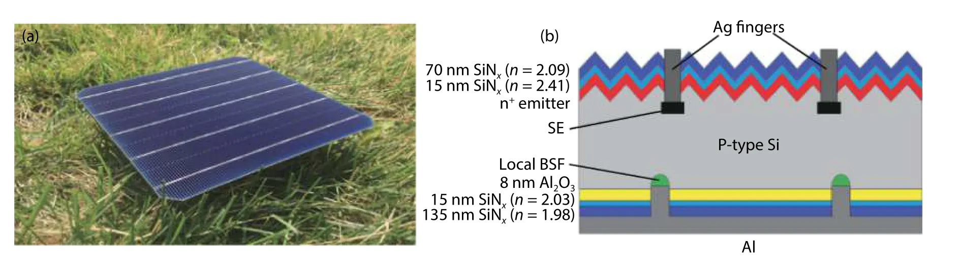
Fig. 1. (Color online) (a) A digital camera image of a PERC solar cell with five busbars from our product line. (b) Schematic illustration of the basic PERC solar cell structure in the simulation.
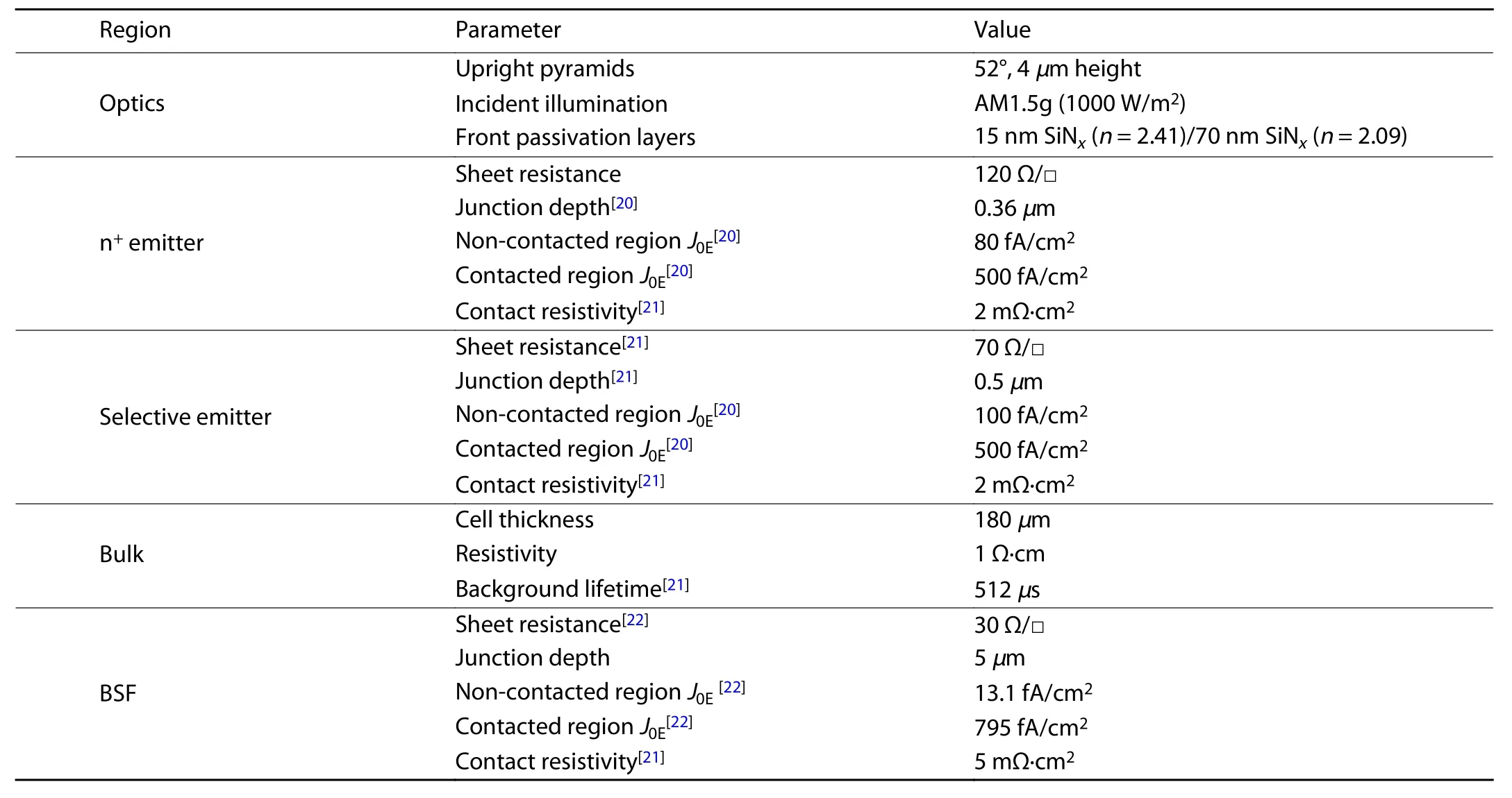
Table 1. Simulation parameters of PERC reference cell.
The PERC solar cell is simulated by Quokka 2 software,which solves the charge carrier transport in a quasi-neutral silicon device[15]. This approach employs simplifications, featuring conductive boundaries and quasi-neutrality condition to the general semiconductor carrier transport model[15]. The conductive boundary condition omits the need to solve the general set of semiconductor equations, consisting of one transport equation for minority and majority carriers and Poisson’s equation for the electric potential[15−17]. The model of charge carrier transport as described by three coupled differential equations[18]can be simplified and therefore solely solved by a set of two differential equations. These simplifications are well validated to not impose notable loss of generality or accuracy for wafer-based silicon solar cell devices[15].
Fig. 1(a) shows a digital camera image of a PERC solar cell with five busbars from our product line. The simulation model (Fig. 1(b)) is configured based on the products. The width of simulated solar cell is 200μm. The solar cell features a front selective emitter (SE) configuration. The emitter is passivated with a double-layered SiNxthin films, in which the refractive index (@632 nm) and thickness of the bottom SiNxare 2.41/15 nm and the top SiNxare 2.09/70 nm, respectively. Al2O3/double-layered SiNxstacked thin films are deposited on the rear side, in which the thickness of Al2O3is 8 nm and the refractive index and thickness of SiNxare 2.03/15 nm,1.98/135 nm, respectively. The generation profile of light to electrical carriers is simulated by Module Ray Tracer from PV Lighthouse, Sunsolve[19].
Table 1 lists the initial parameters of the PERC reference cell, which includes the data acquired from the production line and literatures. Based on the data in Table 1, a 21.90% efficiency reference PERC solar cell is obtained by simulation,which is similar with the mass-produced efficiency as shown in Fig. 2.
3. Results and discussion
3.1. Surface passivation of the emitters
Based on the simulated 21.90% PERC reference solar cell,potential improvements from surface passivation, silicon wafer quality and metal grid line are studied using data from the literature to pave the way for PERC solar cells beyond 24%. In PERC solar cells, the front double-layered SiNxthin films act not only as antireflection layers but also as a passivation layer. This passivation layer has a significant increase on the electrical properties of the solar cell, especially theVOCandJSC. The passivation performance is reflected by the reverse saturation current density (J0E) in the simulated model.The relationship between the recombination current density(Jrec) andJ0Eis given by[23]
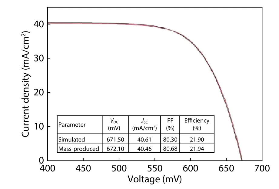
Fig. 2. The J-V curve of PERC reference cell and the electrical properties comparison between simulated and practical mass-produced PERC cell.
wherenandprepresent the concentration of electrons and holes, respectively, andni,effrepresents the effective intrinsic carrier concentration. According to the Eq. (1), reducing theJ0Ewill lead a lower theJrecand a better passivation performance.
In an ideal case, the relationship betweenVOC,JSCandJreccan be expressed by[24]
whereJphis the photocurrent density,Kthe Boltzmann constant,Tthe thermodynamic temperature,qthe electron charge, andvthe voltage. According to the Eqs. (2) and (3),theVOCandJSCincrease as the recombination currentJrecdecreases. Therefore, an excellent passivation layer can effectively increase theVOCandJSCof the cell. In the reference cell,a double-layered SiNxhaving different refractive indices is selected as the front surface passivation layer based on our production line. Besides the double-layered SiNx, Huanget al.systematically studied the passivation mechanism and performance of stacked PECVD SiOxNy/SiNx, thermally grown SiO2/SiNx, thermally grown SiO2/ALD Al2O3/SiNxand ALD Al2O3/SiNx[25]thin films. According to these results, the relationships between the sheet resistance of n+emitter and theJ0Eafter passivation using these four types stacked thin films are summarized in Fig. 3[25,26]. It is seen that the emitters with a higher sheet resistance can be passivated much better.SiO2/Al2O3/SiNxand SiO2/SiNxhave better passivation performance than the SiOxNy/SiNxand Al2O3/SiNx, which delivers aJ0Eas low as 20 fA/cm2as the sheet resistance increased to 120 Ω/□. The Al2O3/SiNxstacked film has a poor passivation performance on n+emitter due to the high effective negative charge density (Qeff= −2.4 × 1012cm−2) in Al2O3[25]. This will repel photogenerated electrons and then result in depletion or weak inversion of the charge carriers under a high surface doping concentration condition[25,27], and in turn an increased recombination at the n+emitter. For the SiO2/Al2O3/SiNxstacked film, the introduction of SiO2layer not only brings a low negative charge density (Qeff= −2.1 ×1011cm−2) but also results in a very low interface state density (Dit= 1010eV−1·cm−2) because of the superior ability of SiO2in passivating the dangling bonds on Si surface[28],which is also called chemical passivation. The excellent passivation result of SiO2/SiNxstacked film (Qeff= 2 × 1011cm−2) can also be attributed to the superior chemical passivation of SiO2which is similar to SiO2/Al2O3/SiNx. The SiOxNy/SiNxstacked film (Qeff= 1.2 × 1012cm−2) has a higher interface state density (Dit= 6.1 × 10¹¹eV−1·cm−2)[29]and so results in a poor chemical passivation compared to SiO2/SiNxstacked film[26].
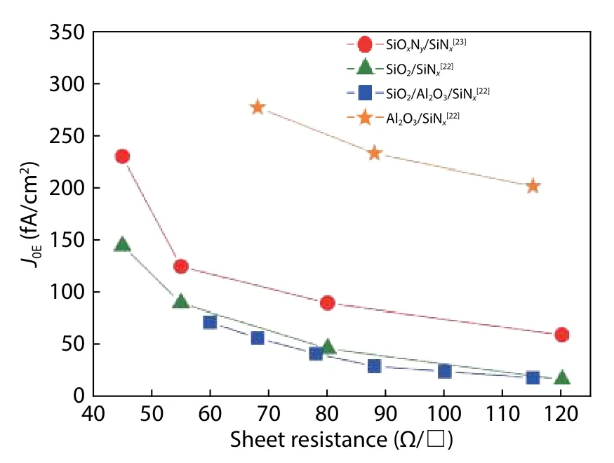
Fig. 3. (Color online) The relationship between the saturation current density J0E and sheet resistance of SiOxNy/SiNx[26], SiO2/SiNx[25],SiO2/Al2O3/SiNx[25] and Al2O3/SiNx[25] passivation layers on n+ emitter of PERC solar cell.
Fig. 4 compares the electrical properties of the four types of stacked films (SiO2/Al2O3/SiNx, SiO2/SiNx, SiOxNy/SiNxand Al2O3/SiNx) that are used in the PERC model. The thickness and refractive index of the double-layered SiNxand the simulation parameters are consistent with the reference cell, while all SiO2, SiOxNy, Al2O3in the four stacked films are 7 nm. It is seen that theVOCand FF are positive dependent on theJ0E.Although a lowerJ0Ecan benefit photocurrent, the optical parasitic loss seems dominant and leads to decreasedJSC.Eventually, the device using SiO2/SiNxhas the highest efficiency of 22.22%, which is 0.32% higher than that of the reference cell, while the cell using Al2O3/SiNxhas the lowest simulated efficiency of 21.35%. Therefore, in the subsequent optimization process, SiO2/SiNxstacked film is selected as the emitter passivation layer.
3.2. Quality of the silicon wafer
A silicon wafer with high carrier lifetime is of great benefit for improving solar cell efficiency. The carrier lifetime is inversely proportional to the recombination rate (R). TheR, as a comprehensive result of Auger, radiative and Shockley-Read-Hall (SRH) recombination, which can be expressed as[24]
whereRAugeris the Auger recombination rate derived from the research of Richter[30]. The radiative recombination is described by the product of hole concentrationp, electron concentrationnand radiative recombination coefficientBrad. SRH recombination is given by[31,32]
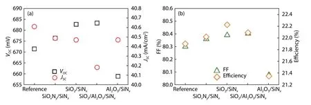
Fig. 4. (Color online) Comparison of (a) simulated efficiency and VOC, (b) simulated JSC and FF of PERC solar cells using different n+ emitter passivation stacked layers.
wheren1=ni,effexp[(Et−Ei)/kT],p1=ni,effexp[−(Et−Ei)/kT],Etis the defect level,Eiis the intrinsic level, andτn0andτp0represent the lifetime of electrons and holes, respectively.τn0/p0=(vthσNt)−1, where the average thermal motion ratevth= 1.1 ×107cm/s,σis the capture section of the defect recombination center for electron/hole, andNtis the defect concentration. The last part in the Eq. (4) represents for the recombination caused by a fixed; that is, injection independent, bulk minority carrier lifetimeτb,fixed.
In boron-doped p-type silicon wafers, the BO complex defect is an important SRH recombination center affecting carrier lifetime of the silicon wafer. Fig. 5 shows the carrier lifetime of p-type silicon wafer of varying resistivity under different conditions of BO complex activity. The intrinsic limit solid curve[33]represents the BO complex-free status while the dashed line and dotted line are the deactivated BO conditions obtained by Walteret al.[34]and Schmidtet al.[35], respectively. It can be clearly seen that the carrier lifetime can be improved through the effective BO deactivated process.
Based on the relationship between wafer resistivity and carrier lifetime shown in Fig. 5, the electrical performance for different wafer resistivity is simulated in Fig. 6. Furthermore,in Fig. 6, the results from Refs. [33-35] are labeled as sample As, Bs and Cs, respectively. It can be seen that the efficiencies,VOCandJSCof all samples increase with increasing wafer resistivity over the range of 0.5-1.5 Ω·cm. When the wafer resistivity increases further,VOCandJSCsaturate gradually for both of Bs and Cs, while efficiencies of Bs show slight decreasing and efficiencies of Cs become saturated. These trends for efficiencies,VOCandJSCare similar with the experimental results[36]. In contrast to the increasing trend of FF in literature 36, all of the FF results for different samples in Fig. 6 show a decreasing trend. This discrepancy can be attributed to the special injection dependence of bulk lifetime. To get the highest solar cell efficiency, the optimum value of the wafer resistivity is around 1.5 Ω·cm. When taking the intrinsic limit lifetime (6200μs)[33], the maximum efficiency of the cell is 22.19%, which is 0.29% higher than that of the reference cell.When the silicon wafer is subjected to an optimum BO deactivated process (2500μs)[34], the highest efficiency of the cell is 22.13%, which is 0.23% higher than that of the reference cell.When the silicon wafer is subjected to a general BO deactivated process(430μs)[35], the maximum efficiency of the cell is 21.85%, which is 0.05% lower than the reference cell. This indicates that a suitable BO “passivation” process is very important to achieve a high-efficiency PERC solar cell. The subsequent optimization process is based on p-type silicon wafer with the resistivity of 1.5 Ω·cm and a corresponding carrier lifetime of 2500μs.
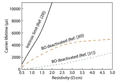
Fig. 5. (Color online) Relationship between resistivity and carrier lifetime of silicon wafer under intrinsic limit condition and different BO deactivated processing conditions[29-31].
3.3. Metal electrodes
In the reference cell, the front grid line uses mainstream five busbars (BB) technology. The busbar width is 700μm,while the width and pitch size of fingers are 38 and 1600μm,respectively. The width of the busbars and the fingers are converted to a whole optical shading width of 57.7μm with a shading factor of 0.69[37]. A shading factor is used to define the effective width of fingers, which can be reduced due to the reflection into the cell through the edges of the fingers and the total internal reflection at the air/glass interface[37,38].
In order to further reduce the series resistance of the cell and improve efficiency, multi-busbar technology (MBB) is expected developed rapidly[39]. The increase in the number of busbars can shorten the conduction distance of the current in the fingers, which effectively reduces the resistance loss and improves the efficiency of the cell. In addition, MBB can reduce the usage amount of silver paste by greatly reducing the width of busbars[40].
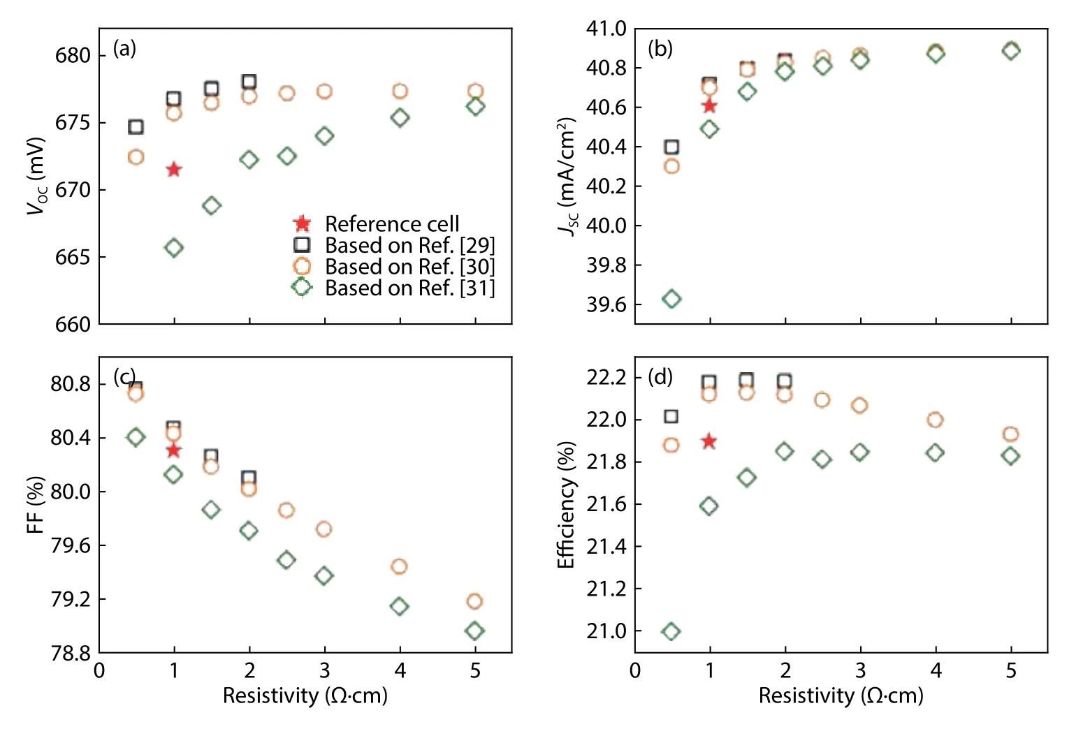
Fig. 6. (Color online) The electrical performance of PERC solar cells varies with the resistivity of silicon wafers under intrinsic limit and different BO deactivated processing conditions[29-31].

Table 2. Comparison of resistivity and contact resistivity of different metal electrode[21].
In the current industrial production of PERC solar cells,Ag paste is generally used in the front screen printing while Al paste is used on the rear side. A multilayer material with higher density and higher conductivity using nickel, copper and other metals based on the electrolysis principle is also used in the metallization scheme[41]. Compared with the traditional screen-print Ag paste, this technology can achieve a thinner grid line and a lower contact resistivity, which can effectively improve the cell efficiency. A comparison of resistivity and contact resistivity of different metal electrode is shown in Table 2.
In the simulation optimization, the front grid line of PERC adopts a 12 BB design. By calculating the total optical shading area of the metal electrodes, combined with the busbar and finger width of 300 and 38μm for 12 BB technology and the shading factor of 0.69[37], the corresponding shading width is 32.6μm. The front metal electrode is deposited by electroplating Ni/Cu with a contact resistivity of 0.1 mΩ·cm2.
Fig. 7 summarizes the three optimization steps of the PERC solar cell. The first step is the n+emitter passivation optimization. According to different passivation layers, the cell using SiO2/SiNxhas the highest simulated efficiency, followed by SiO2/Al2O3/SiNx, SiOxNy/SiNxand Al2O3/SiNx. When using a SiO2/SiNxpassivation layer, the surfaceJ0Ereaches as low as 20 fA/cm2and the cell efficiency reaches 22.22%, which is 0.32% higher than the reference cell. An optimized bulk resistivity of 1.5 Ω·cm is obtained in the second step. The star,rhombic and circle in step (2) are electrical parameters that are based on silicon wafers with carrier lifetimes of 6200,2500 and 430μs, respectively, which are described in Fig. 4.When the carrier lifetime is taken as 6200μs, the simulation efficiency of the cell is 23.13%, which is considered as the limiting efficiency in this step. When the carrier lifetime is 2500μs, the simulation efficiency of the cell is 22.98%. The third step is the optimization of the metal electrodes based on a carrier lifetime of 2500μs. The hollow stars represent the 23.76% efficiency based on the 12 BB technology by which the shading width reduces from 57.7 to 32.6μm. If the screen-print Ag paste is furtherly replaced by the electroplated Ni/Cu electrode with lower contact resistivity of 0.1 mΩ·cm2and width of 32.6μm, the efficiency can be improved to 24.04% thanks to the significant improvement of FF of up to 81.24%, while theVOCandJSCremain constant.These results are represented by solid hollow stars, as shown in Fig. 7.
Based on the free energy loss analysis (FELA) simulation,Fig. 8 shows the analysis of the efficiency loss sources of PERC solar cell between the efficiency of 24.04% and the ultimate limit efficiency of 29% based on the Shockley-Queisser model[42−44]. The recombination loss is the largest (2.73%), followed by the optical loss (1.42%), and finally the ohmic loss(0.81%). Further analysis has found that the individual loss due to the recombination of SRH and intrinsic carriers in the silicon wafer is the largest (0.61%), followed by the individual loss from surface reflection (0.54%), and then from parasitic absorption (0.51%). These individual losses sum up to an efficiency of 27.51% rather than to the ultimate limit of 29%. The rest efficiency gap is due to the synergistic effect that the increase ofJSCwill result in increasingVOC, and hence will increase the efficiency. The synergistic efficiency enhancement over the whole ohmic improvements and optical improvements are only 0.03% and 0.18%, respectively, while the synergistic efficiency enhancement over the whole recombination improvements is as high as 1.49%.
4. Conclusion

Fig. 7. (Color online) Simulated solar cell of a possible scenario for further PERC cell improvements. In step (1), the star, triangle, circle and rhombus points represent cells with SiO2/SiNx, SiO2/Al2O3/SiNx, SiOxNy/SiNx and Al2O3/SiNx, respectively. In step (2), the star, rhombus and circle points represent carrier lifetimes of 6200, 2500, and 430 μs, respectively. In step (3), the hollow star represents the cell with 12 BB and the solid star represents the cell using 12 BB together with Ni/Cu electrode.
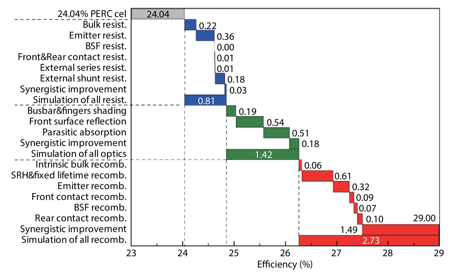
Fig. 8. (Color online) Sources of the efficiency loss between the simulated PERC solar cell with 24.04% to the limit efficiency of 29%.
A reference PERC solar cell with 21.90% efficiency is obtained from numerical simulation based on the data from the production line. Its electrical properties are well coincided with that of the practical solar cell. Based on the reference cell, the performance as a function of surface passivation,quality of silicon wafer and metal electrodes was systematically discussed. By comparing the passivation layers, SiO2/SiNxstacked thin films are considered to be the best candidates for the passivation of n+emitters because of their low optical parasitic loss and excellent passivation properties. By considering both the passivation of BO complex and the relationship between resistivity and minority carrier lifetime, silicon wafers with resistivity of 1.5 Ω·cm and carrier lifetime of 2500μs are preferred. For metal electrodes, the 12 BB technology and Ni/Cu electrode are employed with an optimal shading width of 32.6μm and contact resistivity of 0.1 mΩ·cm2. Finally, a PERC model with an efficiency of 24.04% is obtained.In addition, an analysis of the efficiency loss sources from the 24.04% simulated efficiency to the 29% ultimate limit of PERC solar cell is performed. It can be seen that there is still much room for optimization in terms of surface reflection loss, absorption loss and SRH recombination loss. Therefore, this work is expected to give a guideline for the design and manufacture of high-efficiency PERC solar cells.
Acknowledgments
This work was supported by the National Natural Science Foundation of China (No. 61504155).
杂志排行
Journal of Semiconductors的其它文章
- Low on-resistance 1.2 kV 4H-SiC power MOSFET with Ron, sp of 3.4 mΩ·cm2
- Mathematical analysis of organic-pass transistor using pseudo-p-OTFTs
- An 18-bit sigma -delta switched-capacitor modulator using 4-order single-loop CIFB architecture
- Variation tolerance for high-speed negative capacitance FinFET SRAM bit cell
- 1064 nm InGaAsP multi-junction laser power converters
- A high performance adaptive on-time controlled valley-currentmode DC-DC buck converter