Variation tolerance for high-speed negative capacitance FinFET SRAM bit cell
2020-06-18YaqianQianShushanQiaoandRongqiangYang
Yaqian Qian , Shushan Qiao , and Rongqiang Yang
1University of Chinese Academy of Science, Beijing 100049, China
2Institute of Microelectronics of the Chinese Academy of Sciences, Beijing 100029, China
Abstract: Negative capacitance FinFET (NC-FinFET) has a promising developmental prospect due to its superior performance in SS < 60 mV/dec (subthreshold swing), especially in SRAM. Noise margin is an important metric to evaluate the performance for SRAM, together with static leakage, read speed, etc. In this paper, we study the effects of the variation of ferroelectric material(thickness, polarization), FinFET critical physical parameters (fin number, channel length) and some ambient factors (working temperature, supply voltage) on the performance of NC-FinFET SRAM within the reasonable fluctuation tolerance range. The SRAM bit cell is analyzed with a basic 6T structure. The impact of fin number and channel length for NC-FinFET SRAM is different from that of conventional FinFETs. Additionally, the ferroelectric material and some other factors are assessed in detail.
Key words: negative-capacitance FinFET (NC-FinFET) SRAM; variation; noise margin; speed
1. Introduction
The structure of NC-FinFETs is almost the same as Fin-FETs, but the NC layer is positioned between the gate and internal gate, whose structure is MFMIS (metal-ferroelectric-metal-insulator-semiconductor) as shown in Fig. 1[1]. Compared to another structure - MFIS (metal-ferroelectric-insulatorsemiconductor), it can effectively avoid hysteresis under most cases. Negative capacitance FinFETs (NC-FinFETs) could operate at a sub-60-mv/dec subthreshold swing, as shown in Fig. 2, and a high on-current[2]. Articles[3-5]have introduced the compact model consisting of BSIM-CMG and Landau-Khalatnikov (L-K) equations, simulation flows, and characteristics of NC-FinFET, especially in Ref. [6], for a single transistor. The variation of ferroelectric material and some parasitic factors have been deeply analyzed, but the variation tolerance for cell level has not been estimated. As SRAMs occupy a major portion of chip area, a new study to replace FinFETs with NCFinFETs is meaningful. Two factors: static noise margin (SNM)and write margin (WM) are the main metrics to evaluate the performance of SRAM, and the trade-off between them has always existed. Besides, to estimate the standby state, leakage measurement is essential.
In this paper, we study the effects of the variation of ferroelectric material (thickness, polarization), FinFET critical physical parameters (fin number, channel length) and some ambient factors (working temperature, supply voltage) on the performance of NC-FinFET SRAM with high read speed.
2. Device structure and simulation scheme
Fig. 3 is a schematic of a traditional 6T bit-cell consisting of NC-FinFETs. This paper will study the performance of SRAM based on the above structure, how to analyze the internal factors and find a better balance will be carried out through the simulation process of Fig. 4. Firstly, the ferroelectric materials commonly used in NCFETs are perovskite ferroelectrics. These materials have good stability. The local temperature is about 500 °C. Therefore, even at high temperatures of 125 °C, The negative capacitance characteristics remain the same, and the performance will not abruptly change due to this temperature. Static noise margin (SNM) is the term used to determine the stability of the SRAM cells. The SNM is the tolerance of the maximum noise voltage for the cross inverters output nodes and the minimum amount of noise to ensure the state is maintained[7]. For the simulation graphic,SNM is defined as the side of the smaller square that can be fitted inside the "eye" of the butterfly stability. Large SNM means the cell will not be disturbed easily during the read operation. The write margin (WM) is the maximum bit-line voltage to flip the node from 1 to 0[8]. The larger the WM is,the faster the write speed will be. SNM and WM are separately associated with the ratios of pass gate transistor (PG),pass down transistor (PD) and pull up transistor (PU) on-currents, the former can be presented asand the latter asThe drive voltage and current are difficult to control because of the variation of a single device, so by modifying the negative capacitance material, the basic features of the FinFET or the other conditions, the performance of SRAM will be quite distinguishable.
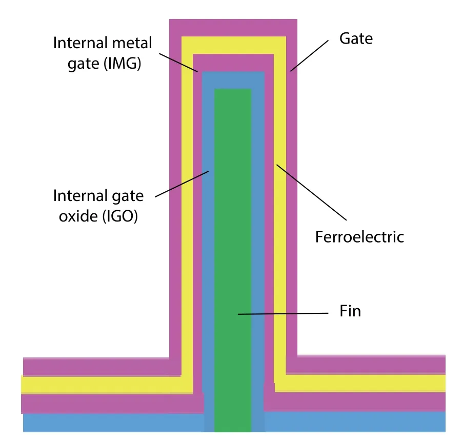
Fig. 1. (Color online) the structure of NC-FinFET.

Fig. 2. (Color online) The subthreshold swing improved by NC compared to the baseline.

Fig. 3. The schematic of traditional 6T SRAM-cell.

Fig. 4. The simulation flow chart for analysis the performance variation for the 6T SRAM, and the compact model is the BSIM-CMG cooperating L-K equations.
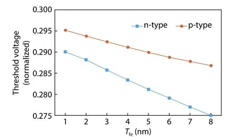
Fig. 5. (Color online) The VT mismatch between n-type and p-type NCFinFET under the same process: when the thickness of ferroelectric material increases, the mismatch gets worse.
Even under the same process, n-type and p-type transistors present different performances, especially the threshold voltage (VT). Fig. 5 confirms the above conclusions. It can be seen that as the thickness of the ferroelectric increases, theVTmismatch between the two transistors becomes more serious. The threshold voltage of the ferroelectric material is negative, so theVTof a NC-FinFET will be lower compared to the baseline FinFET. The threshold voltage of the device is the minimum voltage required to turn on the transistor,which is closely related to the gate control capability of the device itself. The study of this work is based on the actual taped-out FinFET data, the mismatch between n-type and ptype transistors is small, but asTfeincreases, theVTvariation degree of the two is not consistent due to the difference of the carrier transport mechanism between them. The grid-control capability of n-type NC-FinFETs will become weaker with the increase of ferroelectric thickness, while the p-type will be relatively slow. So, as theTfeincreases, theVTmismatch will increase. In order to observe the tolerance variation on cell level, the same change will be applied for the whole SRAM cell. To evaluate the stability of NC-FinFET SRAM cells,first of all, under a fixed FinFET baseline and working environment, by changing the ferroelectric material the single transistor showed that as the thickness of the ferroelectric decreased, the negative DIBL phenomenon will be more apparent. A suitable choice of polarization is difficult to a certain extent, so in this work we refer to the parameters in paper[9]. Having found appropriate NC parameters, the modification for the baseline FinFET is carried on to determine whether or not the changing trend of NC-FinFET SRAM is similar to the baseline FinFET SRAM. Increasing fin number to boost the drive current of SRAM is the industry technique, so changing the fin number in cooperation with baseline SRAM will be verified. Furthermore, a perfect channel length could be optimized in a different technology generation, and this factor will also be analyzed. Finally, we will discuss some other impact after discovering the best parameters for NC-FinFET SRAM. In Ref. [10], conclusions can be drawn that the SNM of SRAM tends to decrease with the increasing temperature, and the WM shows the opposite tendency. Besides, the supply voltage is limited. Although a large drive voltage is beneficial to speed, it will lead to the power consumption of the SRAM cell increasing exponentially. Therefore we will find out the smallest supply voltage for NC-FinFET SRAM to work normally.
3. Results and discussion
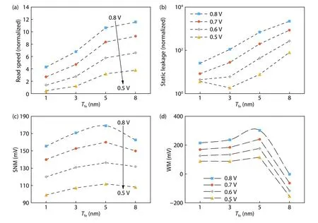
Fig. 6. (Color online) (a) Read speed, (b) leakage, (c) SNM, and (d) WM of NC-FinFET SRAM influenced by the thickness of ferroelectric material.
Followed by all the above simulation flows, some phenomena can be observed from the graphs. Firstly, we will study the integration of ferroelectric material and basic FinFET even though the polarization is difficult to extract from the figure, while the recently proposed SPICE model of ferroelectric material in Ref. [11] utilizes a very complex circuit to express the nonlinear dependence ofVFEupon polarization (P).Pis self-consistently equal to gate charge (Qg) of the FinFET.Hence, the model is independent of FinFET parameters[12].We choose the appropriate parameters to make sure the ferroelectric works well. Considering the industry process, unitive(uniform) change will be implemented in the whole SRAM cell consisting of different transistors. Secondly, the larger thickness of the ferroelectric material (Tfe) improves the read speed distinctly as has been shown in Fig. 6(a). An explanation for this phenomenon is that the ferroelectric works perfectly with the baseline in a reasonable range and the conclusions related withTfein Ref. [13] are almost the same. The influences on other performances-static leakage, SNM and WM-is shown in Figs. 6(b)-6(d). The changing tendency between static leakage andTfeis same, so a small thickness is needed for ultra-low power SRAM. Differing from the single change trend, the SNM and WM is fluctuant with increasingTfe. When the thickness of the ferroelectric is 5 nm, SNM reaches its maximum value. As the thickness of the ferroelectrics continues to increase, SNM decreases; the main cause of this phenomenon is the largeVTmismatch in SRAM. Consistent with the trend of SNM, WM shows a declining trend whenTfeequals 5 nm. In order to avoid an unstable state, 1 to 3 nm is the best choice. In this range, the SNM and WM is relatively balanced without a large trade-off between them.The formula is listed to further investigate the influence ofTfeto the cell:
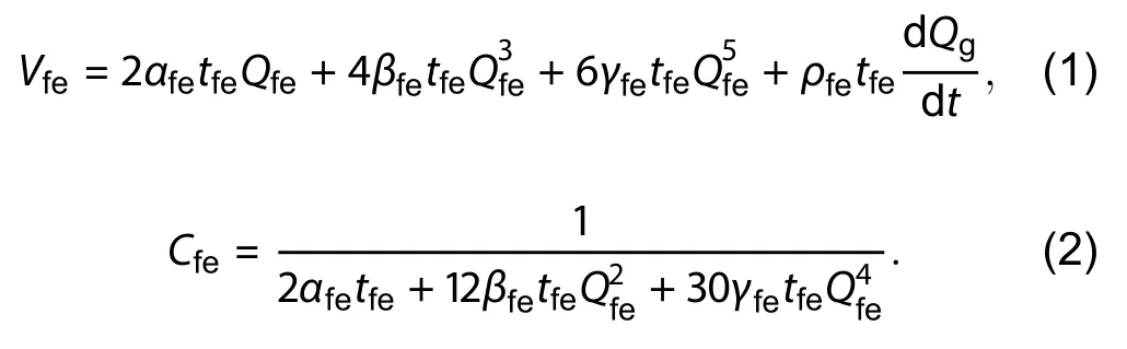
Refs. [14, 15] explain that theCFEshould be a little larger thanCbaseline, and the large discrepancy will lead to a mismatch between negative capacitance and FinFET capacitance, while the coefficient is fixed, so the thicker the ferroelectric material becomes, more serious the mismatch problem will be. The work function is associated with the gate structure, so the relationship between ferroelectric and baseline needs further research. Furthermore, the reliability is still unclear.
Secondly, having fixed the parameters of ferroelectric material, in this part, we have analyzed the critical metrics of the baseline. As with the above operation, all the changes are the same for the whole SRAM cell. Increasing the fin number(Nfin) of the NC-SRAM cell, the influences basically conforms to the baseline. In detail, read speed is remarkably improved since the increase ofNfincontributes to the current, as shown in Fig. 7(a). Meanwhile, in Fig. 7(b), the leakage problem gets worse because increasing the fin number is equivalent to making the width longer, resulting in the leakage path being broadened. Some other metrics are shown in Figs. 7(c) and 7(d), the change of SNM and WM is not evident, but we can still see that when the fin number is only 1, both of them are better. The tendency is not parallel to the baseline, so the fin number of NC-FinFET should harmonize with the baseline SRAM cell. Another parameter: channel length (Lg) is also vital to the NC-FinFET SRAM cell. In principle, the read speed will slow down while theLgincreases for the reason that the voltage and current controlled by gate is enhanced in a short-channel device. The NC-SRAM cell optimizes the read speed well obeying the above rules. In the cell level, the leakage problem is presented in Fig. 8(b), the leakage problem is gradually improved because the short channel will lead to larger junction leakage. The more detail causes can be deduced from the formula[16]:

Fig. 7. (Color online) (a) Read speed, (b) leakage, (c) SNM, and (d) WM of NC-FinFET SRAM influenced by the fin number of baseline with fixed FE thickness 3 nm.

Fig. 8. (Color online) (a) Read speed, (b) leakage, (c) SNM, and (d) WM of NC-FinFET SRAM influenced by the channel length of baseline with one fin.
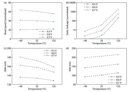
Fig. 9. (Color online) (a) Read speed, (b) leakage, (c) SNM, and (d) WM of NC-FinFET SRAM influenced by temperature with one fin and supply voltage ranges from 0.5 to 0.7 V.
In the formula, the factor most severely influenced by length isIjunction. So, to some extent, the correspondence between the ferroelectric material and baseline mainly account for the leakage, which means the channel length determines the static power of the cell. From Fig. 8(c), the SNM is almost maintained under the same voltage, but a little abnormal phenomenon occurs when the supply voltage is 0.8 V. To account for this, the SNM can be expressed[17]:

In this paper, the size of the PD, PU and PG are all the same, sorandqare equal to 1. To analyze the influence of the channel length for SNM, theVDDwill be fixed to 0.8 V,then we get following formula:
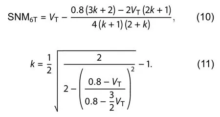
The conclusion can be drawn that in this case, SNM has the same change tendency with theVT, whileVTis almost determined by channel length. So theVTreflects the SNM. Conversely, the WM drops mildly. From all of above, the channel length is not only important to the baseline SRAM but also sensitive to the NC-FinFET SRAM. An appropriate channel length maybe the key factor for the whole NC-FinFET SRAM.Apart from that, in all figures the supply voltage also affects the performance. Most of the metrics conform to normal rules except SNM and WM under special cases. The range of supply voltages ensuring the NC-FinFET SRAM works correctly will be discussed after fixing all the above parameters with best choice. From all the graphics, the best voltage for the cell can be chosen between 0.5 to 0.7 V, making low power significant. Fig. 9 presents the temperature infection. It has been mentioned the structure chosen in this article is MFMIS. The interconnection between the metallic and ferroelectric layers is based on the principle of self-continuity of charge, because the ferroelectric layer and the metal layer share only charge, but the material itself is not compatible.When the temperature is 125 °C, the ferroelectric remains stable and the metal layer will not migrate. Therefore, under reasonably high temperature, the device itself is in a stable state. Read speed is almost flat while static leakage abruptly rises under higher temperature. The SNM declines slightly while WM increases gently.
4. Conclusion
Based on an ordinary and reasonably proper SPICE model of ferroelectrics, the performance of a NC-FinFET SRAM cell is presented. We discussed the variation tolerance for the NCFinFET SRAM cell. A smallTferanging from 1 to 3 nm exhibits a better performance while sacrificing little speed. SmallNfinis the better choice in this paper due to the fact that SNM and WM barely change when the fin number increases but the leakage problem becomes serious. Channel length is limited to within 6 nm, due to the fact that trade-off among leakage, SNM and WM cannot be eliminated, except under small channel length, and the read speed and WM is perfect while the leakage problem can be cleaned up by making NC-Fin-FET SRAM work under a low supply voltage. Therefore, a reasonable supply voltage range is 0.5 to 0.7 V. This work utilizes its low power advantage meanwhile ensuring performance.Considering the application in industry, both low and high temperatures can be tolerated, ranging from -40 to 125 °C which is the detection range commonly used in process.
Acknowledgements
This work was supported in part by the University of Chinese Academy of Science and SMIC
杂志排行

Journal of Semiconductors的其它文章
- Low on-resistance 1.2 kV 4H-SiC power MOSFET with Ron, sp of 3.4 mΩ·cm2
- Numerical study of mono-crystalline silicon solar cells with passivated emitter and rear contact configuration for the efficiency beyond 24% based on mass production technology
- Mathematical analysis of organic-pass transistor using pseudo-p-OTFTs
- An 18-bit sigma -delta switched-capacitor modulator using 4-order single-loop CIFB architecture
- 1064 nm InGaAsP multi-junction laser power converters
- A high performance adaptive on-time controlled valley-currentmode DC-DC buck converter