Magnetic field enhanced radio frequency ion source and its application for Siincorporation diamond-like carbon film preparation
2020-03-09JipingYIN殷冀平QingWANG王庆XinlongWU吴鑫龙ChunyuCHENG程春玉DechunBA巴德纯andZengLIN蔺增
Jiping YIN (殷冀平), Qing WANG (王庆), Xinlong WU (吴鑫龙),Chunyu CHENG (程春玉), Dechun BA (巴德纯),2 and Zeng LIN (蔺增),2
1 School of Mechanical Engineering & Automation, Northeastern University, Shenyang 110819, People’s Republic of China
2 Key Laboratory of Implant Device and Interface Science of Liaoning Province, Northeastern University,Shenyang 110819, People’s Republic of China
Abstract Various ion sources are key components to prepare functional coatings, such as diamond-like carbon(DLC)films.In this article,we present our trying of surface modification on basis of Siincorporation diamond-like carbon (Si-DLC) produced by a magnetic field enhanced radio frequency ion source,which is established to get high density plasma with the help of magnetic field. Under proper deposition process, a contact angle of 111° hydrophobic surface was achieved without any surface patterning, where nanostructure SiC grains appeared within the amorphous microstructure. The surface property was influenced by ion flow parameters as well as the resultant surface microstructure. The magnetic field enhanced radio frequency ion source developed in this paper was useful for protective film applications.
Keywords: magnetic field enhanced radio frequency ion source, Si-incorporation diamond-like carbon film, microstructure, hydrophobicity, protective film
1. Introduction
During the last 50 years,DLC films have been deposited with various vacuum plasma techniques [1, 2]. By applying appropriate facilities as well as processing parameters, qualitative films are obtained to meet the technical challenge. In addition to the well-known mechanical,electrical,optical and chemical properties [3, 4], hydrophobicity is also very important and it is required by many applications such as optical windows or lenses. To do so, DLC films have been incorporated with other elements like silicon and fluorine to modify the bonding structure and chemical composition in the amorphous carbon matrix, and hence to influence wettability of the surface[5-8].Among them,Si-incorporation into DLC films is known to reduce their wettability and residual internal stresses[7,8],and it is also used to improve their optical and electrical properties as well as hemocompatibility and biocompatibility [9]. Grischke et al found that Si-incorporation into DLC films could observably decrease the surface energy from 42 to 31 mN m−1[5]. Si changes the content of sp2-C and sp3-C, causing the films better hydrophobicity, however the mechanism is not clear. Proper content and bonding of C and Si on the topmost surface of the films can result in the high contact angle. Moreover, Si-DLC films are reported to have low-friction and low-wear performance, which offer a promising solution for long term stability problem.
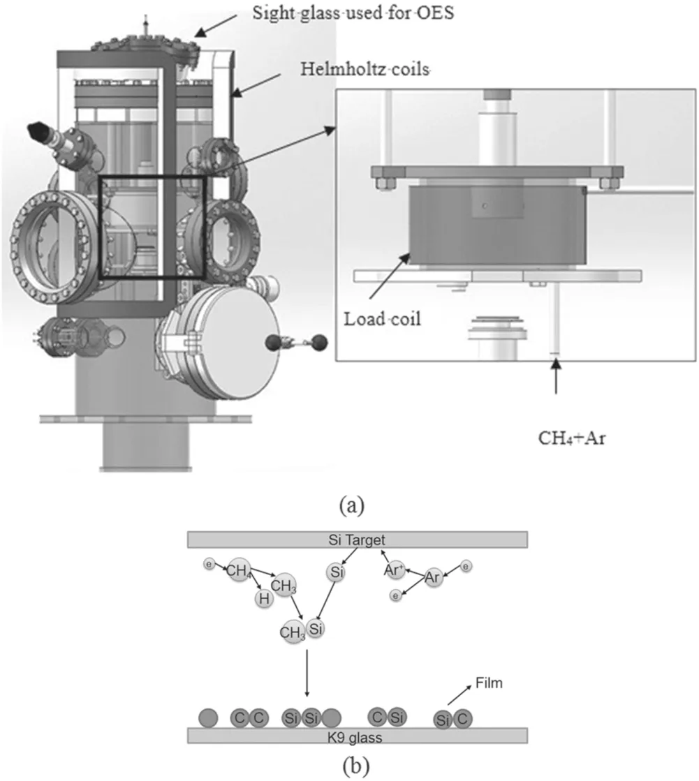
Figure 1.(a) Schematic diagram of magnetic field enhanced radio frequency ion source, (b) the deposition process of Si-DLC film.
As to the preparation technique as well as the related facility, numbers of researches on the coating preparation have been published, applying a variety of activation and deposition technology, such as plasma enhance chemical vapor deposition(PECVD), radio frequency (RF) plasma beam chemical vapor deposition and magnetron sputtering [10-13]. However, there was little Si-DLC researches prepared by high density, homoenergetic ion source, which have had great potential for large scale and high feasible industrial application.
In our previous works, DLC films were prepared by conventional RF-PECVD[4,12].This article reports the new try of Si-DLC films deposition with low-energy ion flows from an magnetic field enhanced RF ion source. A low pressure at 10−2-10−1Pa was pumped by a turbo-molecular pump, the ionic species energy can be varied by adjusting the RF sputtering power of the ion source,while nearly independently adjustment of the ion flux. With the help of the RF ion source, the ion energy can be reduced to several tens of electron volts, and the ion current density is maintained at about 1 mA cm−2. As a consequence, the deposition of films can be sustained at a remarkable growth rate (on the scale of μm h-1).
Plasma diagnostic techniques were used to monitor the excitation and de-excitation processes in various plasmas, such as optical emission spectroscopy(OES),Langmuir probe and so on. The main purpose of this study is to investigate the mechanism of a new magnetic field enhanced RF ion source as well as its application on hydrophobic Si-DLC films preparation.Several complementary techniques are used to characterize the microstructural and properties of the resultant films.
2. Experimental procedure
Figure 1(a) shows the home-made vacuum plasma coating facility.Plasma is generated in the ion source by a 13.56 MHz RF power supply through a single turn coil mounted outside the cylinder(diameter = 100 mm,and height = 60 mm).The horizontal direct current (DC) magnetic field is generated by two coils with distributed windings around the chamber (not shown in figure 1(a)).By varying the DC current of the coils,the strength of the DC-magnetic field can be varied. Another RF power supply is applied to vary the ion energy, which provides the possibility of controlling the ion flow and ion energy independently [14, 15]. The substrate holder
(r = 20 mm) is located just below the ion source.
As to the plasma status diagnosis, the optical emission spectroscopy was used to obtain the base line information of the Ar plasma.At this experiment,the Ar flow rate = 8 sccm and RF1 power = 300 W, while the field coil current was varied from 3.9 to 4.5 A to study the influence of the magnetic field on plasma properties.
For the film preparation application, the base pressure in the chamber was typically below 8.0 × 10⁻⁴Pa before a deposition process was started.Before the deposition of film,the substrate was cleaned for 30 min with an Ar plasma generated by the magnetic field enhanced radio frequency ion source with the RF power at 300 W and Ar flow rate at around 6 sccm.During deposition process,the pressure in ion source was maintained at approximately 3 Pa, while the pressure in the coating chamber was only 8.0 × 10⁻²Pa. Subsequently,high purity(99.99%)CH4and argon were introduced into the chamber at the 1:1 flow ratio. And then the sputtering power was applied to the Si target (99.999%) for the preparation of Si-DLC.
The Si-DLC deposition process may be understood with the help of figure 1(b). High density plasma is generated by the magnetic field enhanced radio frequency ion source,where Ar ions and CHxions are accelerated towards both the Si target and the sample holder. In this experiment, Si-DLC film was deposited at a rate of approximately 65 nm min−1with a final thickness of about 130 nm. In addition, different amount of doped Si in DLC were obtained by changing the sputtering power from 40 to 80 W. For convenience, we use Sl, S2, S3, S4 and S5 for the samples deposited at the sputtering power of 40, 50, 60, 70 and 80 W, respectively.
A micro fiber spectrometer (EPP-2000, Stellar Net,America)was used to record the optical emission spectra.An optical fiber was guided through the center of the chamber window to collect the spectral data.The microstructure of the deposited film was studied using Raman spectroscopy with the wavelength of 488 nm, where a low input power of 3.5 mW was used to reduce the possible laser-induced heating effect. In order to characterize the bonding states of the film,x-ray photoelectron spectroscopy (XPS) with an Al Kα monochromatic excitation source with energy of 1486.6 eV was employed at 150 W. The surface morphology was evaluated by field emission scanning electron microscope (FESEM). Moreover, transmission electron microscopy (TEM)and selected-area electron diffraction (SAD) were employed to investigate the textured structure of the SiC phase in the resultant Si-DLC film.
It is very interesting that with the help of this ion beam assisted deposition process,a hydrophobic surface was achieved without any surface patterning.A contact angle meter(SL200B,Kino,America)was used to monitor the surface wettability with the sessile drop method. Each specimen was measured at 22 °C ± 1oC and 50% ± 5% RH at four different points. The measurements could be repeated within ±2°. The durability of the DLC-coatings was investigated by the friction test using a pin-on-disk tribometer at a high load under rotating motion.The radius of rotation was 3 mm and rotational speed was 168 rpm.An eraser (Polyvinylchloride and polystyrene) of 3 mm in diameter and around 2.0 μm RMS in surface fniishment was fxied on a holder.The friction was measured with strain gauges under the load of 1000 g,and the results were analyzed on a computer.Optical transmittance was measured with a UV/visible spectrophotometer (DR/4000U, Perkin-Elmer, USA).
3. Results and discussion
3.1. OES for glow discharge Ar-plasma diagnosis
Figure 2(a) shows the emission spectra of Ar-plasma for the field coil current at 4.1 A from 650 to 1050 nm.The strongest emission lines were expressed as Ar I due to the excitation of neutral argon atoms and a succedent spontaneous decay.Furthermore, the Ar II lines visible in figure 2 are derived from the emission of singly charged Ar+ions [16]. Similar spectra were obtained for other field coil currents situation.Figure 2(b) shows the variations of the total emission intensity with the field coil current. It can be seen that the total emission intensity reached the maximum as the field coil current was increased to 4.1 A. At this point, the coating chamber appears the brightest glow discharge during the test,which implies that magnetic field enhanced radio frequency ion source reaches at the electron cyclotron wave resonance situation.
3.2. Microstructure and chemical bonding analysis
Figure 3 shows FE-SEM images of the deposited Si-DLC film by the magnetic field enhanced radio frequency ion source under the sputtering power of 40 and 80 W. Each of the Si-DLC coated samples in the experiment is very smooth and flat, indicating that surface topography will not bring the so called ‘amplification factor’ for the wettability of the surface in our previous work [4, 17].
The vibrational modes of the chemical bonding of C and Si atoms in Si-DLC films were investigated by Raman spectroscopy.The Raman spectra of the S1 specimen(shown in figure 4)consist of a weak peak at 480 cm−1, which corresponds to the vibration of amorphous silicon(a-Si)[18].The crystalline silicon has no peak at 520 cm−1, which indicates that a part of Si was doped into the films in the form of Si-Si under these deposition conditions and probably grew in the form of amorphous silicon.Two separated Raman peaks at 796 and 972 cm−1correspond to the longitudinal optical (LO) mode and the transversal optical(TO) mode of SiC structure, which are actually consistent with the reported for 3C-SiC(β-SiC)[19].The characteristics at high wavenumbers of the range 1000-1800 cm−1is connected with the vibration of DLC graphitic feature, generally including the phonon vibration of sp2-C (G peak) at 1580.15 cm−1and the disorder-allowed zone edge mode of graphite (D peak) at 1362.36 cm−1, manifesting the feature of amorphous carbon flims [20]. Similar spectra were found for the other flims. All spectra were ftited with the combination of two Gaussians for the G and the D peaks. And the a-Si peak became weaker and SiC peak became stronger with the increase of the sputtering power (shown in fgiure 4). These results indicate that the deposited flims change from Si-Si bonding dominant to a Si-C bonding composition.
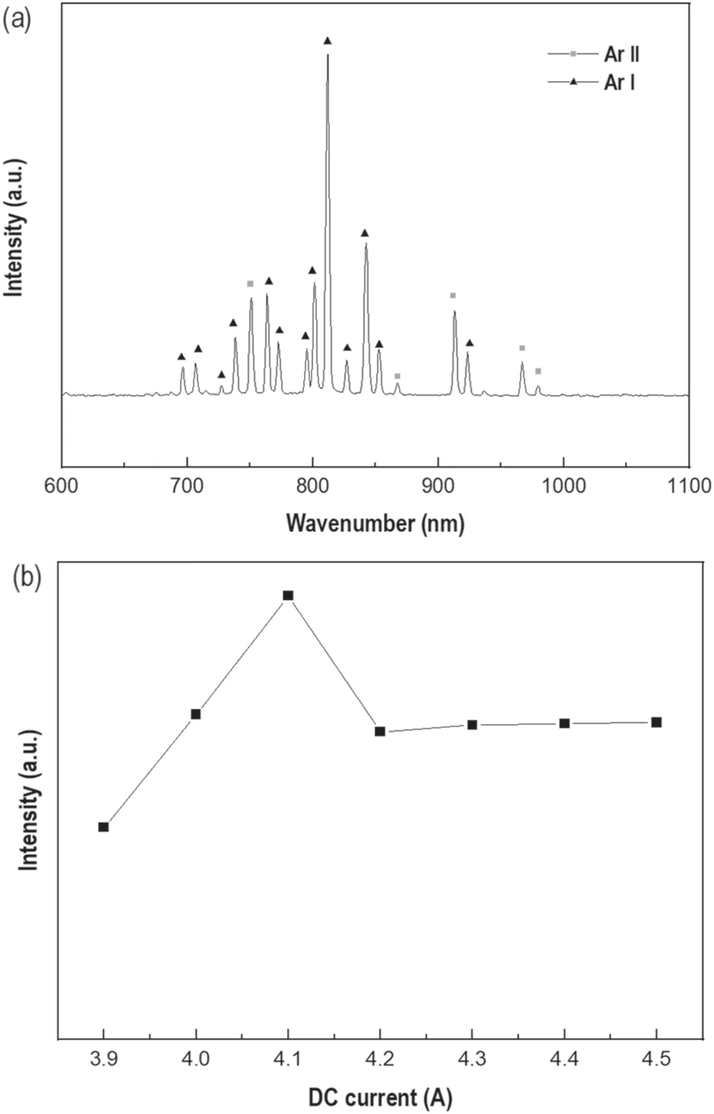
Figure 2.(a) Optical emission spectrum between 650 and 1050 nm for field coil current ∼4.1 A, (b) the variations of the total emission intensity with the field coil current.

Figure 3.SEM micrographs of Si-DLC films deposited at the sputtering power of (a) 40 W and (b) 80 W.
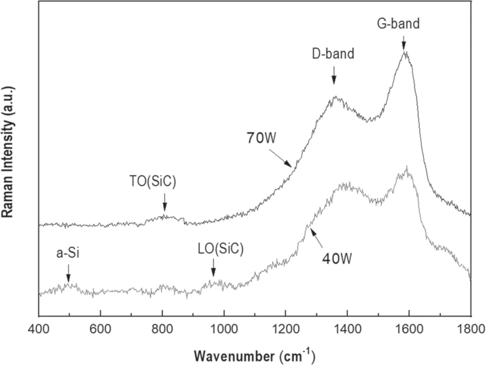
Figure 4.Raman spectra of the S1 and S4 specimens.

Figure 5.(a) I(D)/I(G) ratio, (b) the position of the G band, as a function of the sputtering power at 40-80 W.
In general, the shift of the G peak and the peak intensity ratio I(D)/I(G)of the fixed G-band (1580.15 cm−1) to D-band(1362.36 cm−1) showed opposite behavior with the sp3/sp2bonding ratio, manifesting the physical properties of DLC films [21, 22]. Figure 5 shows the evolution of the G peak position and the I(D)/I(G)values with the sputtering power.When the sputtering power was ascended to 60 W both the G peak position and the I(D)/I(G)values rose to the maximum.It is suggested that the content of sp2-C in the films was probably maximized [23]. Due to the low sputtering power, the plasma energy and the sputter yield of Si are very low. The interaction among the plasma is not strong, resulting in the incorporation of Si into the film in the form of amorphous silicon. Although there is a little SiC formed in the film,which is not enough to have a large impact on the sp3-C content, so sp2-C content appears dominant in the resultant film.Since plasma energy increases with the sputtering power(below 60 W), the groups in the plasma will collide more intense and split more thoroughly.As a result, the number of dangling bonds formed on the surface increases,and H atoms and ions implanted into the surface also increases.In the end,the increasing opportunities for H and sp3-C to interact lead to the conversion of sp3-CH2to sp2-C=C, and heat release accelerates this process, resulting in a decrease in the proportion of sp3-C. When the sputtering power increases to above 60 W, the plasma energy is high enough to form Si-C for most Si to increase the content of sp3-C [24].

Figure 6.(a) C 1s and (b) Si 2p XPS spectra of the S4 specimen(power at 70 W).
To further obtain qualitative information on the Si-DLC films, XPS analysis was employed. The XPS spectra of C 1s and Si 2p are shown in figures 6(a) and (b), respectively, of the S4 specimen (power 70 W). The highest energy in the region of 284-284.5 eV is ascribed to the C-C bonding formed from carbon matrix in the film. The C-Si (C ls) and Si-C (Si 2p) configurations, corresponding to bonding between carbon and silicon atoms in SiC,are in the ranges of 282.3-283.7 eV and 99.8-101.3 eV, respectively [25]. The lowest energy in the range of 99.2-99.6 eV stands for the bonding of Si-Si.It is believed that Si is incorporated mainly in the form of SiC, while the sputtering power becomes higher.The XPS result shows that silicon concentration of the S4 specimen was about 14.0 at%.
Figure 7 shows the bright field TEM image and dark field micrograph of Si-DLC film deposited at different sputtering powers. In figure 7(b), there are a large number of dispersed nanograins (in general spherical nano-sized particles,corresponding to spherical macroparticles in figure 7(a)) and ribbon-like crystal regions (black ribbons in figure 7(a)),which indicates that crystalline structure is enclosed in the amorphous carbon matrices. There are two crystalline phases in the film which are revealed by the diffused cloudy electron diffraction pattern.These can be indexed as(2 0 0)and(3 1 1)reflections from SiC. In figure 7(c), there are a large number of ribbon-like crystal regions and little dispersed spherical nano-sized particles. Both the number and the size of grains increase with the sputtering power. Combining the Raman and XPS data, we believe that the deposited Si-DLC film exhibits a reticular structure consisting mainly of SiC and a-C:H.

Figure 7.(a) The bright field TEM image, (b) dark field micrograph of Si-DLC film deposited at 70 W and (c) dark field micrograph of Si-DLC film deposited at 80 W (Red arrows point to ribbon-like crystal regions and green arrows point to nanograins).The insert picture shows the electron diffraction pattern.

Figure 8.Contact angle of the Si-DLC films as a function of the sputtering power at 40−80 W.
3.3. Wettability and frictional properties
The evolution of water contact angle (WCA) of the Si-DLC films with sputtering power is shown in figure 8.The WCA of the substrate(K9 glass)is 51°,while the WCA of the Si-DLC coated specimens is increased to be mostly above 100° with the highest value of 111°, which indicates that the Si-DLC films deposited in this paper have good hydrophobic property.
A few of factors will affect the surface wettability,including surface topography, presence of functional groups and the presence of sp2and sp3bonding in the resultant Si-DLC film.Since the surface of the resultant Si-DLC film is very smooth, the follow analysis is focused on the effect of the microstructure on hydrophobicity. As we can see from figure 8, the WCA of the films increases with the sputtering power and reaches the maximum value at 60 W; then it decreases. Raman results (shown in figure 5) indicate that with the sputtering power increasing (≤60 W), more sp2hybridized carbon bonds are formed. Therefore, it seems that hydrophobicity benefits from the microcrystalline graphite phase in the film as well as the inclusion of Si-C and Si-Si in the films. It is implied that proper content and bonding of Si in the DLC film may result in the high contact angle. When the sputtering power continues to increase (≥60 W), the content of sp2-C in the film will decrease gradually. In other words, the number of microcrystalline graphite in the film decreases, and the contact angle of the sample surface decreases. At the same time, the change of surface energy depends on the composition and bond structure of solid phase surface, and the presence of hydrogen and oxygen can affect the adsorption state of reagents on solid phase surface. With the increase of power, the number of dangling bonds on the surface of DLC films increases, which will increase the formation probabilities for hydroxyl groups on the surface and make the hydrophobicity of the films worse.

Figure 9.Frictional coefficient of substrate (a) and DLC coated samples deposited by different powers (b).
Figure 9 illustrates the variation of frictional coefficient of the deposited Si-DLC film as well as the substrate. The reduction of frictional coefficient(from 0.54 down to 0.30)is attributed to the deposited DLC film.Moreover,the whole Si-DLC films exhibited different frictional behavior due to the different chemical bonding in the films.For the specimens Sl and S5,the frictional coefficient change is smaller than that of the others,likely owing to the proper bonding ratio of Si-Si/Si-C and sp3/sp2in the specimens (shown in figure 5).

Figure 10.The SEM images of wear scar on Si-DLC films in different sputtering powers: (a) 40 W, (b) 70 W and (c) 60 W.
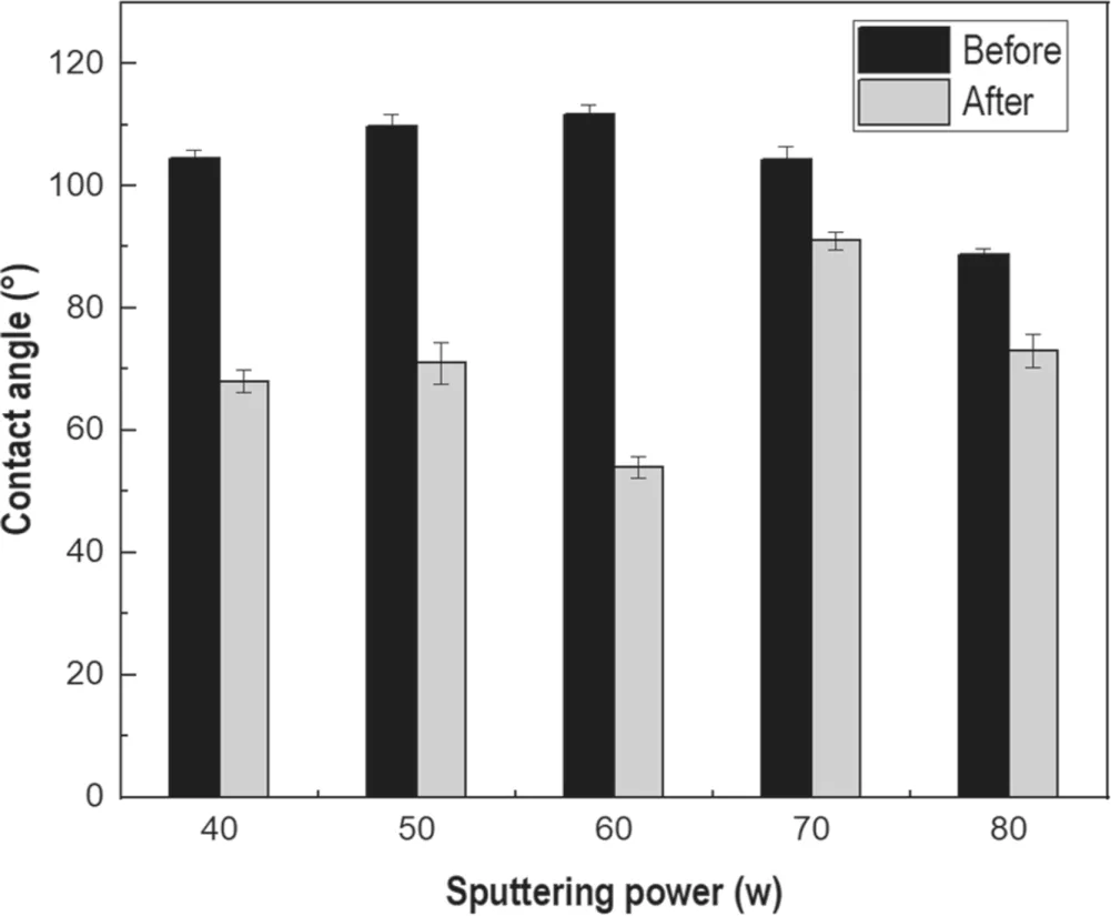
Figure 11.Contact angle of the Si-DLC films as a function of the sputtering power at 40-80 W before and after frictional test.
After frictional testing, a transferred film was visible on the surface of the erasers,which can effectively prevent direct contact between the surface of eraser and the coated specimen, thereby reducing the frictional coefficient and prolonging the service life. The S1 specimen (power 40 W) has the lowest frictional coefficient, meanwhile the coated surface(shown in figure 10(a)) was very smooth without any wear tracks. In figure 10(a), some eraser crumbs (the white bands)are found, because the erasers are soft and the surface of the eraser is very rough. With frictional test continuing, the erasers particles were gradually polished. The frictional coefficients of specimens S2-S4 are observed to be higher at the similar level, which decreased with time. The surface of the eraser is very rough,lead to a high frictional coefficient at the initial stage. With test continuing, the surface were gradually polished,resulting in the friction coefficient decreased.Moreover, the transferred film can effectively prevent direct contact between the coated specimen and the surfaces of eraser, thereby further reduce the frictional coefficient. In figure 10(b), many wear tracks and the eraser crumbs are found on the S4 specimen, which implies that the film had been worn out.Similar phenomenon was found on the surface of the specimens S2 and S5.Figure 10(c)shows the surface of the S3 specimen, which was smooth without any eraser crumbs.
The frictional behavior may correlate with the microstructure of the resultant Si-DLC film, i.e. the coefficient of friction increases with the I(D)/I(G)value [26]. When sputtering power over 60 W, both the friction factor and the I(D)/I(G)values decrease with the increase of the sputtering power. The variation of frictional behavior may lie on the higher content of sp3-C and SiC grains, which reduced the deformation of the films and the coefficient of friction.
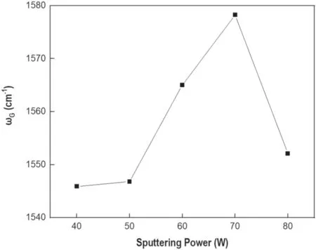
Figure 12.The position of the G band as a function of the sputtering power at 40-80 W after frictional test.
The interrelation between sputtering power and contact angle before and after frictional test is shown in figure 11.It is indicated that the contact angle decreased obviously after the frictional test, owning to the microstructure variation of the films (shown in figure 12). Comparing figure 5(b) with figure 12, it can be found that G peak position of all specimens decreases, which indicates that the content of sp2-C decreases after frictional test, and the content of sp3-C remains in the film, so the contact angle decreases in various degrees. Moreover, it can be seen from figure 10 that the surface topography of samples at low power (≤60 W)becomes smoother after frictional test, so their contact angle is also affected. It is shown that hydrophobicity is not only related to the composition, but also to the surface morphology. It is strange for S3 (60 W) specimen, where the position of the G-band changed from 1597.03 to 1565.16 cm−1and the contact angle changed from 111.7°± 1.5° down to 54°± 1.8°. The change of G peak position is extremely abnormal, indicating that the films may be worn out, so it should be ignored. When the power exceeds 60 W, the film deformation is small and the contact angle maintains well.The contact angle of the S4 specimen is maximum (91°± 1.5°) after frictional test in this experiment.
4. Conclusions
A magnetic field enhanced radio frequency ion source was successfully established and OES diagnosis showed that the total emission intensity reached resonance condition at proper parameters, where the plasma luminescence appeared at the brightest intensity. To check the performance of this homemade ion source system, Si-DLC films were deposited to get the hydrophobic surface for the protective application. The resultant film is very smooth and flat, while Si successfully doped into DLC films.More interestingly,SiC particles were embedded in the amorphous carbon matrices and shown as nanograins and ribbon style.The obtained Si-DLC is likely to be a specific composite layer,containing an amorphous DLC phase and constituting a matrix with islands of nanocrystalline phase of SiC and Si. The observed properties are highly dependent on the microstructure of the resultant films. The coated samples showed good hydrophobicity before scratch test; however, the durability needs to further strengthen for better long-term stability in the future.
Acknowledgments
This work was supported by National Natural Science Foundation of China (No. 51775096); Fundamental Research Funds for the Central Universities, China (No. N141008001/2); and the grants (Y17-0-003 and F16-080-8-00) from Shenyang city.
猜你喜欢
杂志排行
Plasma Science and Technology的其它文章
- Analysis of the characteristics of the plasma of an RF driven ion source for a neutral beam injector
- Synthesis of vertical graphene nanowalls by cracking n-dodecane using RF inductivelycoupled plasma-enhanced chemical vapor deposition
- Application of persulfate in low-temperature atmospheric-pressure plasma jet for enhanced treatment of onychomycosis
- Microwave frequency downshift in the timevarying collision plasma
- Comparison of Reynolds average Navier-Stokes turbulence models in numerical simulations of the DC arc plasma torch
- Effects of fast ions produced by ICRF heating on the pressure at EAST
