Investigation of radiation influences on electrical parameters of 4H-SiC VDMOS
2019-01-17LiShengXuZhiyuanWeiJiaxingLiuSiyangSunWeifeng
Li Sheng Xu Zhiyuan Wei Jiaxing Liu Siyang Sun Weifeng
(National ASIC System Engineering Research Center, Southeast University, Nanjing 210096, China)
Abstract:The radiation influences on electrical parameters of 4H-SiC vertical double-implanted metal-oxide-semiconductor field effect transistor (VDMOS) are studied. By simulations on SRIM software and SILVACO software, the electrical parameters shifts of the device with defects in different regions are observed. The results indicate that the defects in different regions induced by radiations lead to different degradations of the electrical parameters. Non-ionization bulk defects in the JFET region make the drain-source on-state resistance Rdson increase, and those near the impact ionization center make the breakdown voltage Vbreakdown increase. Moreover, the radiation-induced SiC/SiO2 interface defects, known as negative interface charges or positive interface charges, influence the electrical parameters significantly as well. The positive interface charges along the SiC/SiO2 interface above the channel region lead to a decrease in threshold voltage Vth, Rdson and Vbreakdown, while positive interface charges along the SiC/Metal interface above the main junction of the terminal only leads to the decrease in Vbreakdown. The negative interface charges along the SiC/SiO2 interface above the channel region can make Vth, Rdson and Vbreakdown increase.
Key words:4H-SiC VDMOS; radiation; trap; interface charge; electrical parameters
The SiC device has become one of the most promising candidates in power electronic fields due to its high blocking voltage, low power loss and high working temperature[1-3]. Also, it has immense potential to be widely used in the aerospace industry. Since the space environment is extremely harsh, it is significant to comprehensively consider the radiation influences upon the SiC device. As one of the most widely used SiC devices at the moment, 4H-SiC vertical double-implanted MOSFET (VDMOS) is of great investigation value in radiation-resistant fields[4].
Cosmic particles, such as protons, damage the device via different mechanisms. For the bulk region, when the device is exposed to space environment, incident particles can enter the device and impact the lattice atoms with energy transfer, thus making atoms ionize or displace. As the bandgap of the SiC material is so large that the ionization cannot be the main source of damage, the displacement dominates the damage[5]. The displacements of lattice atoms can induce instable vacancies in SiC materials. Parts of the vacancies disappear since the lattice atoms have adequate energy to allow simple damage to regrow back into its original crystalline form. The rest vacancies form deep level defects in SiC materials[6]. It has been proved that the deep level defects in 4H-SiC materials are accepter traps[7]. For the SiC/SiO2interface region, the incident particles can break fragile bonds and bring charges to the interface when passing through it. The type of radiation-induced interface charges in 4H-SiC nMOS capacitor interfaces have been proved to be negative[8]. However, the types of radiation-inducedQeffin different interface regions of power VDMOS are unknown.
Numerous articles have illustrated the radiation effects on SiC devices. Ref.[9] reported that 4H-SiC diodes show increase in series resistance and blocking voltage after the proton radiation. Ref.[10] reported that the radiation effects on the SiC/SiO2interface are different from those on Si/SiO2interface. However, the attention paid to the radiation effects on 4H-SiC VDMOS are not enough, especially in the terminal region of VDMOS[11], so comprehensive studies of the radiation reliability are in high demand.
In this paper, the radiation effects on 4H-SiC VDMOS are studied via simulations. First, the non-ionization radiation-induced traps, whose information is obtained by the SRIM software, are added to the bulk region of the device[12]. Moreover, both positive interface charges and negative interface charges are added to the interface region to make the investigation more comprehensive. Then, the electrical parameter shifts are obtained by the SILVACO software. Finally, the mechanisms of the degradations are illustrated.
1 Structure and Simulation
Fig.1 shows the schematic cross section view of the 1.2 kV 4H-SiC VDMOS studied in this paper. The device mainly contains the cells and terminal region. The terminal structure of the device consists of a main junction (connected to the source) and several guardrings. The depth of the drift region is 12 μm with a doping concentration of approximately 9×1015cm-3. The doping concentrations of the main junction, guardrings and p-body are all 5×1017cm-3, and the depth of the main junction, guardrings and p-body are all 0.95 μm.
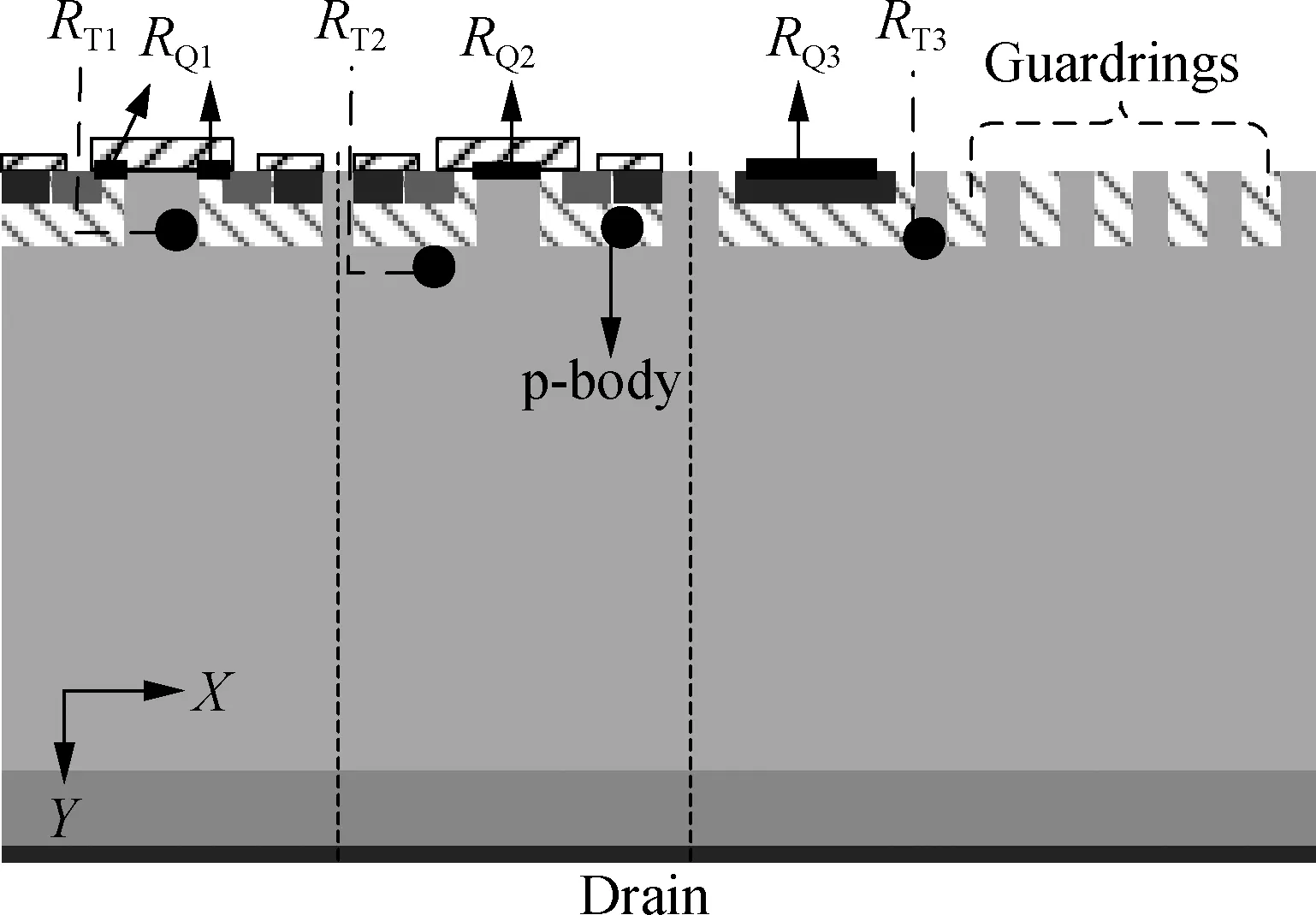
Fig.1 The schematic cross section of the investigated 4H-SiC VDMOS with terminal
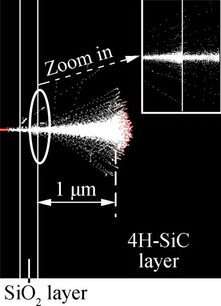
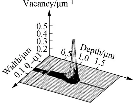
Fig.2(a) shows the typical case of the incident path of 120 keV protons. The incident particles can make target atoms recoil, then the recoiling target atoms cause collision cascades, which dominates the damage process. The transfer of energy occurs during the above process, and the red dots are only plotted if the transferred energy is large enough to displace the atom from its lattice site. Thus, these dots can indicate the main position where the displacements occur[13]. Fig.2(b) shows the ions distribution in the device, which indicates the position of produced defects more clearly. In the case mentioned, the position of the induced defects is about 1 μm beneath the material surface, near the p-body bottom.
(a) (b)Fig.2 Damage process of proton radiation. (a) The incident path of protons; (b) Induced ions distribution
In order to distinguish the influences brought by the damages in different regions, the energy and incident angle of the particles are changed, and three typical damage regions are selected (see Fig.1). The region marked asRT1is located in the JFET region, where the current flows through. The region marked asRT2is located under the p-body region, where the impact ionization center appears, which is observed via simulations. The region marked asRT3is located at the corner of the main junction, where the electric field is usually extremely high. Then the traps are added to the three typical regions to complete the simulations.
The collision cascades can be more serious in the interface region (see Fig.2(a)) and the SiC/SiO2interface is usually of poor quality, thus some fragile bonds can be broken and interface charges can be accumulated at the interface. Whether positive interface charges or negative interface charges will be accumulated at the SiC/SiO2or SiC/Metal interface in the VDMOS is unknown, both positive interface charges and negative interface charges are added into the following three regions to compare (see Fig.1). The region marked asRQ1is the SiC/SiO2interface above the channel region. The region marked asRQ2is the SiC/SiO2interface above the JFET region. Finally, the region marked asRQ3is the SiC/Metal interface above the main junction.
When the defect information has been confirmed, simulations by the SILVACO are completed to acquire the electrical parameter shifts of the device under investigation. What needs to be pointed out is that the surfmob model (the effective field-based surface mobility model) and the aniso impact model (only for 4H-SiC material) in SILVACO are used to ensure the accuracy of the simulation results[14].
2 Results and Discussion
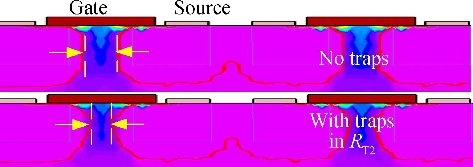
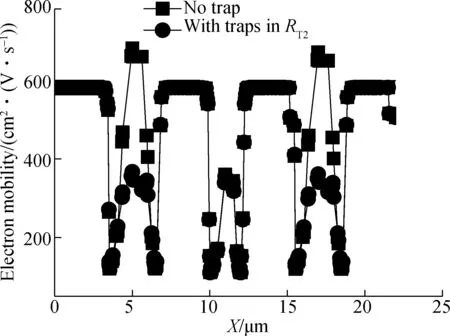
Fig.3 shows variations in the drain-source on-state resistanceRdsonand breakdown voltageVbreakdownof the investigated device. To be noted,Rdsonis extracted atVgs=18 V andVds=5 V, andVbreakdownis extracted atVgs=0 V andIds=100 μA.Rdsonincreases significantly with the increase of the trap density when the traps exist inRT1. To better understand this phenomenon,Vgsis set to be 18 V andVdsis set to be 5 V. Then, the current density and depletion distribution of the device with/without traps inRT1are obtained. Also, the electron mobility along p-body
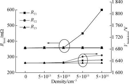
Fig.3 Variations in Rdson and Vbreakdown with the increase in trap density
bottom is extracted (see Fig.4(b)). With the electron captured by the traps inRT1, the electrons density decreases and the depletion layer expands to the JFET region, which leads to narrowing of the current path (see Fig.4(a)). The electron mobility decreases at the same time due to the traps. As a result, the current that reaches the electrode decreases andRdsonincreases. The results are consistent with those in Ref.[9]. However,the traps have no influence onVth, since they cannot influence the inversion layer under the channel region.
(a)
(b)Fig.4 On-state information of the device with traps. (a) Current density distribution; (b) Extraction of electron mobility
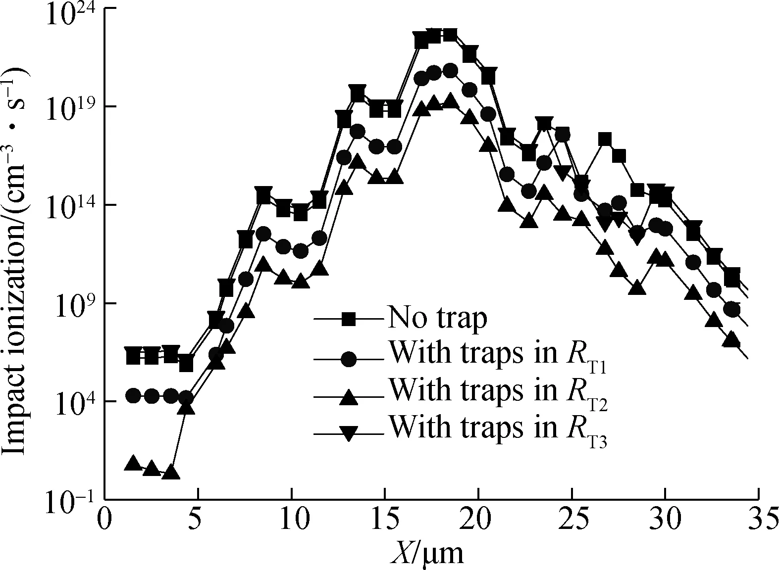
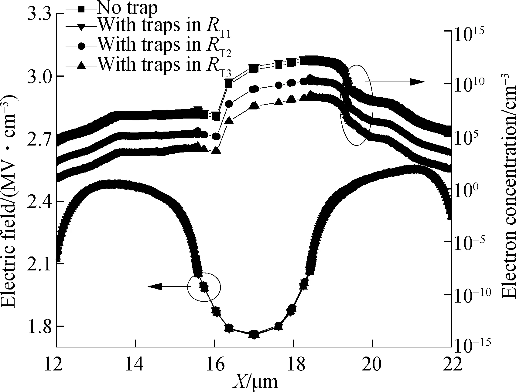
Vbreakdownincreases when the traps exist inRT1andRT2. From the simulations of the four conditions with different trap densities, it can be observed that the peak impact generation value appears in the same location but with different values (see Figs.5(a) and (b)). The electric field and electrons concentration along p-body bottom are extracted to understand these phenomena, as shown in Fig.5(c). The values of the electric field of the four conditions are the same, but the values in the electrons’ concentrations are different. It means that electrons are captured by the traps and few electrons join in the impact ionization process, leading to the decrease in the generated current. As a result,Vbreakdowngradually increases. Moreover, when the traps are closer to the impact ionization center,Vbreakdownwill increase more.
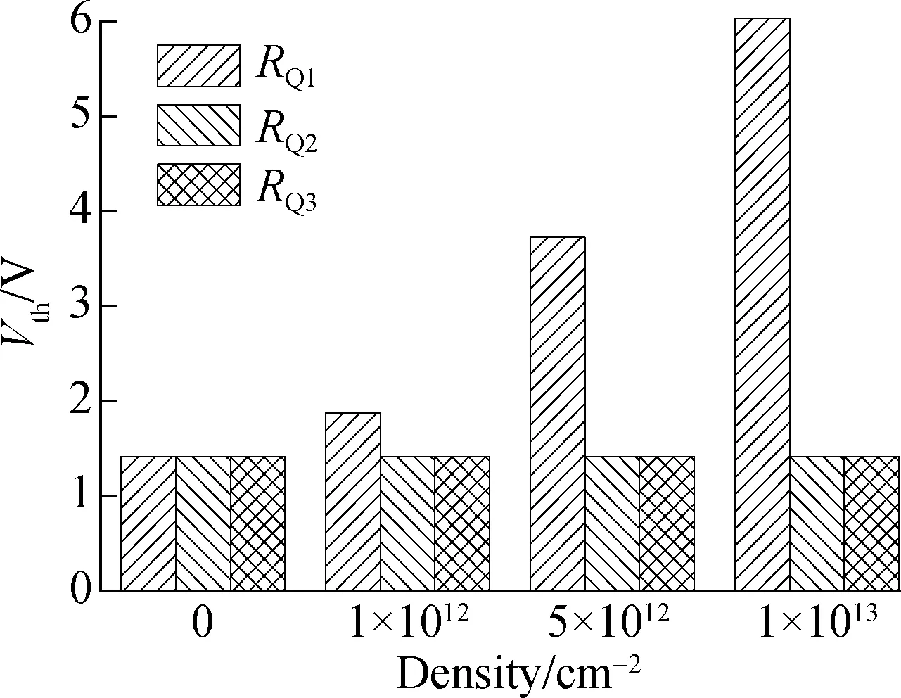
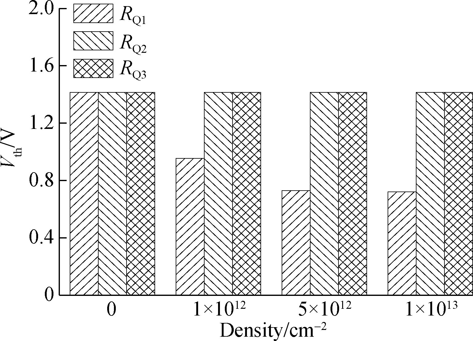
Fig.6 shows the variations of the values ofVth,RdsonandVbreakdownwhen negative interface charges exist. To be noted,Vthis extracted atVds=1 V andIds=0.1 mA. It can be seen from the picture that electrical parameters change only when negative interface charges exist inRQ1. The negative interface charges can reduce the potential in the channel region, and then prevent the inversion process

(a)
(b)
(c)Fig.5 Off-state information of the devices with traps. (a) Impact ionization distribution; (b) Extraction of impact ionization; (c) Extraction of electric field values and electron concentrations
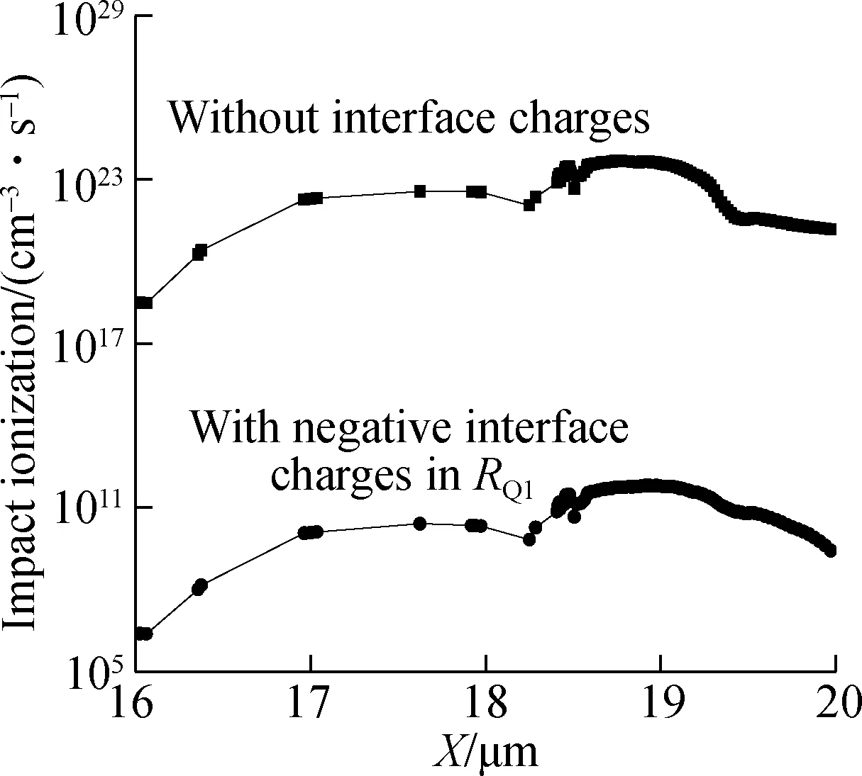
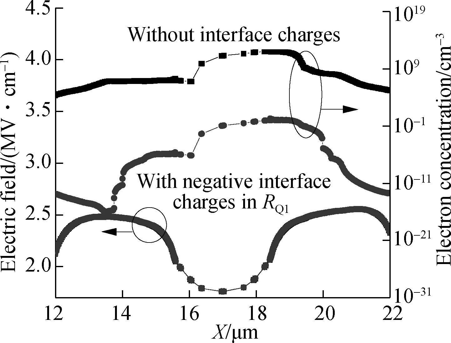
in the channel region. Moreover,VthandRdsonare determined by the inversion degree. When the negative charges exist in the channel region, the inversion degree is reduced, and the channel width can be decreased. The vertical cutting line is applied to obtain the electrons’ concentrations in the channel region (see Fig.7). The result indicates that the channel width is narrower and the carrier concentration in the channel is lower when negative interface charges exist inRQ1, thusVthandRdsonincrease. Then,RIG, electrons concentration, and current density distribution are extracted to understand the increase ofVbreakdown, as shown in Fig.8. It needs to be classified that the impact ionization center is the same as that shown in Fig.5(a), so a part of the curve is shown in Fig.8(a). The ionization-produced current path is just belowRQ1, so the potential along the current path is lower when negative interface charges exist, influencing the impact process and making the decrease ofRIGmax. Therefore,Vbreakdownincreases in spite of the unchanging electric field. For other conditions, negative interface charges are distant from the current path, so the impact process cannot be influenced andVbreakdownremains unchanged.
(a)
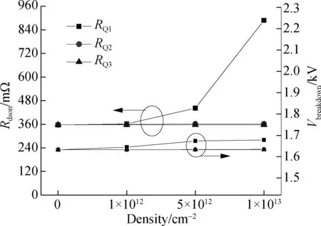
(b)Fig.6 Static electrical parameters of the device with negative interface charges. (a) Variations in Vth when the density of negative interface charges increases; (b) Variations in Rdson and Vbreakdown when trap density increases
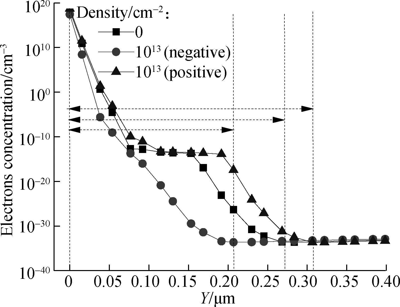
Fig.7 Electron concentrations in the channel region of the device with interface charges
Fig.9 shows the variations ofVth,RdsonandVbreakdownwhen positive interface charges exists. As positive interface charges inRQ1increase the potential and attract electrons into the channel region, the electron concentration in the channel region is larger and the channel width is wider (see Fig.7), thusVthandRdsondecrease.Vbreakdowndecreases significantly when positive interface charges exist inRQ1. The positive charges can increase the potential at the interface and influence the distribution of carriers, thus influence the impact ionization process. The impact ionization distribution in Fig.10 indicates that positive interface charges inRQ1makes the impact ionization center move to the interface, andRIGmaxis much higher. In this way,Vbreakdowndecreases significantly.
(a)
(b)
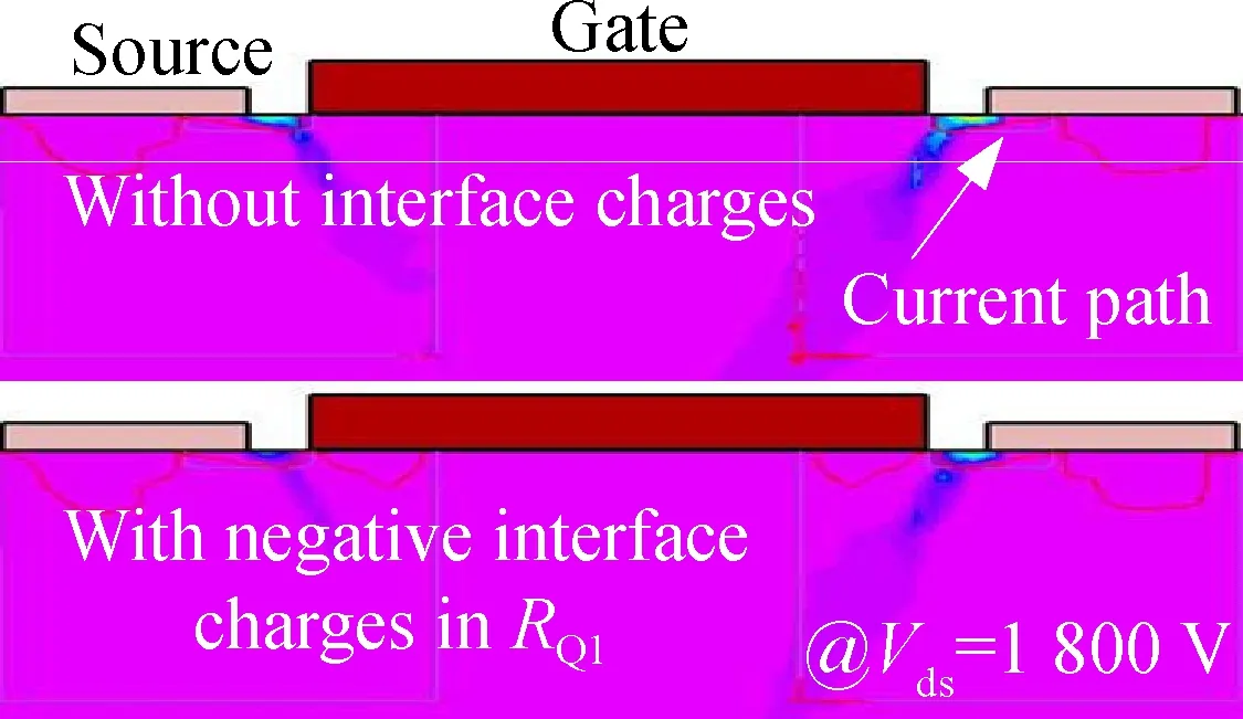
(c)Fig.8 Off-state information of the device with negative interface charges. (a) Extraction of impact ionization; (b) Extraction of electron concentration and electric field values; (c) Distribution of current density after breakdown
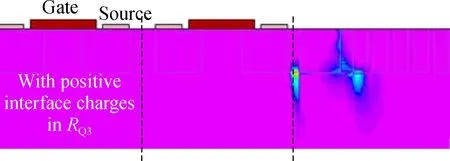
The decrease ofVbreakdownis also observed when positive interface charges exist inRQ3. The distribution ofRIGmaxand the current density are acquired to illustrate the phenomena. As shown in Fig.11, the impact ionization appears between the main junction and p-body when positive interface charges exist inRQ3, and the current generated during impact ionization flows to the electrode along the main junction edge. It means that positive interface charges inRQ3increase the potential under the main junction and attract more electrons, thus enhancing the impact process and makingVbreakdowndecrease.
3 Conclusion
The radiation influences on electrical parameters of 4H-
(a)
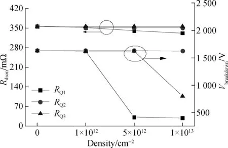
(b)Fig.9 Static electrical parameters of the device with positive interface charges. (a) Variations in Vth when the density of positive interface charges increasing; (b) Variations in Rdson and Vbreakdown when charge density increasing
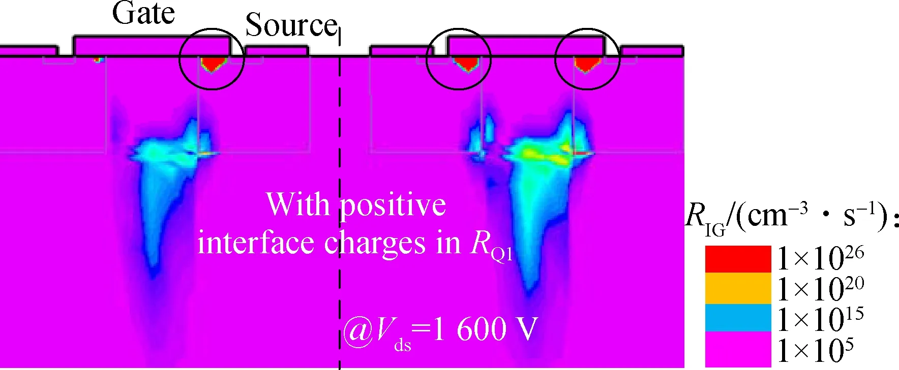
Fig.10 The impact ionization distribution
(a)

(b)Fig.11 Off-state information of the device with positive interface charges. (a) Impact ionization distribution; (b) Current density distribution
SiC VDMOS are studied. For bulk damages, the radiation-induced accepter traps in the JFET region makeRdsonincrease, and the radiation-induced accepter traps near the impact ionization center makeVbreakdownincrease . For interface damages, the radiation-induced negative interface charges above the channel region repulse electrons, thus makingVth,RdsonandVbreakdownincrease. In contrast, the radiation-induced positive interface charges above the channel region attract electrons and makeVthandRdsondecrease. Moreover, these positive charges can make the impact ionization center move to the SiC/SiO2interface above the channel region. As a result,Vbreakdowndecreases significantly. However, the positive charges above the main junction make the impact ionization center move to the bottom of the main junction and attract more electrons there, thus intensifying the impact process and decreasingVbreakdown. To make the 4H-SiC VDMOS more available in aerospace industry applications, the device structure or process should be optimized. The direct method is increasing the passivation layer thickness to reduce the incident particle energy. Moreover, using appropriate materials can be more efficient, for example, Al2O3has more intrinsic traps, which can recombine the radiation induced charges, so it is more appropriate for the passivation layer than SiO2and Si3N4.
杂志排行
Journal of Southeast University(English Edition)的其它文章
- Failure load prediction of adhesive joints under different stressstates over the service temperature range of automobiles
- A game-theory approach against Byzantine attack in cooperative spectrum sensing
- Dependent task assignment algorithm based on particle swarm optimization and simulated annealing in ad-hoc mobile cloud
- A cooperative spectrum sensing results transmission scheme with LT code based on energy efficiency priority
- An indoor positioning system for mobile target tracking based on VLC and IMU fusion
- A simplified simulation method of friction pendulum bearings
