一种牺牲层工艺中金属电极保护方法研究*
2017-09-06张照云唐彬彭勃陈颖慧熊壮苏伟
张照云,唐彬,彭勃,陈颖慧,熊壮,苏伟
(1.中国工程物理研究院电子工程研究所,四川绵阳621999; 2.中国工程物理研究院超精密加工重点实验室,四川绵阳621999)
一种牺牲层工艺中金属电极保护方法研究*
张照云1,2*,唐彬1,2,彭勃1,2,陈颖慧1,2,熊壮1,2,苏伟1,2
(1.中国工程物理研究院电子工程研究所,四川绵阳621999; 2.中国工程物理研究院超精密加工重点实验室,四川绵阳621999)
为了在牺牲层工艺中保护金属电极不被腐蚀,提出了一种利用铝层保护金属电极的方法。在试验中采用了两种铝保护层厚度300 nm和1μm,在两种腐蚀液体4NH4F∶1HF∶2甘油和1HAC∶1NH4F中进行了试验,通过试验表明,铝金属层在两种腐蚀液体中都能够有效保护金属电极,延长牺牲层的腐蚀时间。最后,通过SOI微加速度计加工工艺进一步验证了该方法的有效性。
微电子机械系统;微加速度计;牺牲层刻蚀;金属电极保护
In recent years,the SOI(Silicon on Insulator) material which has a monocrystalline structure layer is fast gaining prominence in the development of MEMS devices[1-6].In the SOIMEMSmicromachining process,the release of the structures is the last processing step.Any patterning with the structures freestanding is difficult to implement,due to the destructive effects of the spinning of resist on the delicate structures.Moreover,any deposited materials can get lodged underneath the freestanding structures.Therefore,when the sacrificial etching takes place,the metal pad,needed to connect the electronic components and the micromechanical structures,will have to be present on the wafer.
The hydrofluoric acid(HF)or buffered hydrofluoric acid(BHF)is the most commonly used etchant for silicon dioxide sacrificial layer etching,because these etchants provide a high selectivity between the sacrificial oxide and the siliconmechanical layers and a high etch rate,which is necessary to perform large underetching in a reasonable period of time.
A problem arises,as the etchants HF and BHF etch themetal pad aswell as the sacrificial oxide.During the etching of silicon dioxide sacrificial layer,many pinholes can be found on the metal pad after a certain etching time.As the etching time increases,the number of pinholes increases.When the time is further extended,some electrode shed[7].Therefore,themetal pad must be protected.
Various approaches have been brought forward to deal with this problem.Literature[8]introduced usingPECVD silicon nitride to protect aluminum interconnect,this layer can be deposited at 300℃.However,this method is too complicated,which needs two extra depositions and two extramasks,and PECVD silicon nitride shows many mechanical defects in the form of pinholes,through which the etchant could reach the aluminum and ruin the aluminum interconnect.Photoresist is usually used to protect themetal pad,but photoresist is not strong enough and limiting the maximum etch time to around 10min.For the long wet etches,the resist needs a complete postbake.And the adhesion of the photoresist layer to the surface of the chip is the another problem.A weak bond can cause the resist to separate from the surface,allowing etchant to seep in underneath and attack the underlying aluminum[7-8].From literature[9-11],by the addition of glycerin or glycerol to the BHF can increase the selectivity between aluminum and the sacrificial layer.For example,literature[11]add glycerol to BHF solution with the proportion of 4NH4F∶1HF∶2glycerol in volume and heating the etchant solution to 55℃~65℃while constantly agitating it with a magnetic stirring bar,has significantly increased the selectivity,resulting in a etching selectivity of 600 to 1 between silicon dioxide and aluminum.Enlightened by this,this paper investigated the method of using aluminum layer to protect metal pad during the etching of sacrificial silicon dioxide layer.
1 Experiment
Because the etching rate of silicon dioxide layer and aluminum and the selectivity between aluminum and silicon dioxide was investigated thoroughly in literature[11].So in this paper,we just studied the metal pad propertieswith the aluminum protection layer.
Two single-side-polished(110)oriented 100 mm silicon wafers were used to carry out the experiments.Two waferswere fist used lift-offmethod to producemetal pad,which was Tiw/Au with 20 nm Tiw and 200 nm Au.And then one wafer was sputtered with 300 nm aluminum layer,the other wafer was sputtered with 1 000 nm aluminum layer.Two wafer were then manually cleaved into dozens of small pieces about1 cm by 2 cm in dimensions for further experiments.
There were generally two series of experiments.One was the etchant solution of 4NH4F∶1HF∶2glycerol and with the aluminum protection layer of 300 nm and 1 000 nm.The otherwas used the solution with the proportion of 1HAC∶1NH4F(40%)and with the aluminum protection layer of 300 nm and 1 000 nm.The etchant solutions for both groupswere fullymixed.
From literature[11],the selectivity between aluminum and the silicon dioxide sacrificial layer was interrelated with temperature and agitation situation.So during the etching,the etchant solutions agitated with amagnetic stirring bar throughout the process and with a temperature controllable water-bath.
2 Results and Discussion
Selectivity is crucial for MEMSstructures to be left unaffected by the sacrificial layer etch.In the case of poor etch selectivity,the structures are attacked in two possible ways:continuous,homogeneous chemical etching and local dissolution(pitting,intergranular corrosion).There are some methods to inhibit chemical etching of the MEMS structures by the sacrificial layer etchant[12]:
(1)introducing a protection layer,
(2)allowing chemical build-up of a native passivation layer,
(3)adjusting the pH to enhance the selectivity or
(4)adding chemical substances produced in the attack reaction in order to shift the chemical equilibrium
During the sacrificial layer etch,corrosion can occur by the formation of local electrochemical cells,the formation of a porous passivation layer or by propagation of voids and cracks.Some methos to inhibit corrosion are[12]:
(1)improvement of the protection quality of the passivation layer e.g.by adding chemical oxidants to the solution,
(2)suppression of adsorption of reactantmolecules e.g.by addition of surfactants(discussed below in the case of aluminum attacked),
(3)addition of complexing or gelating agents to peptize corrosion products(discussed below),or
(4)reduced stress in the structural layer to avoid stress corrosion.
Based on the above theory,we choose two etchants to increase the selectivity:4NH4F∶1HF∶2glycerol etchant and 1HAC∶1NH4F etchant.2.1 4NH4F∶1HF∶2glycerol etchant
This etchant solution started boiling at about 72℃,and started to become instable around 70℃,resulting in the HF beginning to escape from the system.There is no obvious phenomenon even when heated to 67℃[11],so the temperature is controlled at 65℃.
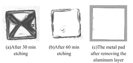
The experiment results are showed in the Fig.1 and Fig.2.Fig.1 is the results of 300nm aluminum protect layer.From the resultswe can see that:(1)after 30min etching,the aluminum protect layer above themetal pad is etched off;(2)after 60 min etching,the whole aluminum protect layer is etched off and themetal pad is kept in good condition.Fig.1 is the results of 1 000 nm aluminum protect layer.From the results we can see that: (1)after a certain etching time,there is air bubble under the aluminum protect layer above themetal pad; (2)when the etching time increase,the air bubble become bigger;(3)after 60 min etching,the aluminum protect layer is not etched off and themetal pad is kept in good condition after removing the aluminum layer.

Fig.1 The results of 300 nm alum inum protect layer with etchant of 4NH4F∶1HF∶2glycerol

Fig.2 The results of 1 000 nm alum inum protect layer with etchant of 4NH4F∶1HF∶2glycerol
From Comparing the two experiment,we can see that the aluminum protect layer can protectmetal pad and prolong the etching time.And the thicker aluminum layer can have a longer etching time.
2.2 1HAC∶1NH4F etchant
It is dangerous to heat up the etchant of 4NH4F∶1HF∶2glycerol.So we use another etchant of 1HAC∶1NH4F to etching silicon oxide sacrificial layer.This etchant can be used in normal temperature and with high selectivity between silicon oxide and aluminum,but this etchant have a lower etching rate of silicon oxide sacrificial layer.
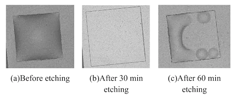
The experiment results are showed in the Fig.3 and Fig.4.Fig.3 is the results of 300 nm aluminum protect layer and Fig.4 is the results of 1 000 nm aluminum protect layer.From the results we can see that:(1)after a certain etching time,there is air bubble under the aluminum protect layer above themetal pad;(2)when the etching time increase,the air bubble become bigger;(3)after 60min etching,the aluminum protect layer is not etched off and themetal pad can be kept in good condition.

Fig.3 The results of 300 nm alum inum protect layer with etchant of 1HAC∶1NH4F

Fig.4 The results of 1 000 nm alum inum protect layer w ith etchant of 1HAC∶1NH4F
From the two experiment A and B,we can see that the aluminum protect layer can protectmetal pad and prolong the etching time in both etchants.And the thicker aluminum layer can have a longer etching time.The 1HAC∶1NH4F etchant has a lower etching rate compared to the etchant of 4NH4F∶1HF∶2glycerol.
3 Application
To test the actual effect of thismethod,a SOI accelerometer device was examined.The devices were released in the solution of 4NH4F∶1HF∶2glycerol.The main fabrication process of using thismethod to produce SOIaccelerometer is shown in Fig.5:(a)The structural layer is patterned with a 3μm thick positive photoresist,then sputter metal film of Tiw/Au on the structure layer,after stripping the photoresist by acetonesolvent,themetal electrode is obtained;(b)By ashing in oxygen plasma to remove the remaining organic residues,the structural layer is sputtered 1 000 nm aluminum layer coveringmetal pad;(c)A 3μm thick positive photoresist is patterned on the aluminum layer,and then etch the aluminum to form the accelerometer pattern;(d)Use DRIE to etch the silicon deep to the oxide layer;(e)Remove the photoresist;(f)Use the solution of 4NH4F∶1HF∶2glycerol to etch the silicon oxide sacrificial layer;(g)Remove the rest aluminum layer.

Fig.5 Themain fabrication process of using this method to produce SOI accelerometer
As the photoresist film was not removed after the structure etching process with DRIE(step(e)),it will serve as an additional etch barrier during the silicon oxide etching process.Because the photoresist without completely postbake to remove all the sovents present in the resist,leaving it relatively soft and porous.To prolong the resist etch time,the resist need a complete postbake after DRIE process.

Fig.6 SEM images of a part SOI accelerometer with good metal pad using 4NH4F∶1HF∶2glycerol etchant to etch the silicon oxide sacrificial layer
Through above method,the devices of SOImicroaccelerometers are obtained successfully.Fig.6 is a SEM image of a part SOIaccelerometer with good metal pad.So thismethod is tested effective through SOI accelerometer fabrication.
4 Conclusion
The paper proposed a method of using aluminum layer to protect metal electrode in sacrificial etching process.By adding glycerol to BHF solution with the proportion of 4NH4F∶1HF∶2glycerol and heating the etchant to 65℃while constantly agitating it throughout the process,the selectivity between silicon dioxide and aluminum can be increased significantly.So using the 4NH4F∶1HF∶2glycerol to etch the silicon dioxide sacrificial layer while protecting the metal pad using aluminum layer,themetal pad can be kept in good condition after release the MEMS structures.When the undercut length needed to etch is of a few microns,we can use the etchant of 1HAC∶1NH4F to etch the silicon dioxide sacrificial layer.This etchant is not need to heat and has a high selectivity between silicon dioxide and aluminum,but has a lower etching rate.And also can use aluminum layer to protectmetal pad when using 1HAC∶1NH4F to etch the silicon dioxide sacrificial layer.At last,to test the actual effect of thismethod,a SOIaccelerometer device was examined and it is tested effective through SOIaccelerometer fabrication.
[1]Li Sainan,Liang Ting,Wang Wei,et al.A Novel SOI Pressure Sensor for High Temperature Application[J].Journal of Semiconductors,2015,36(1):014014-1-014014-5.
[2]Oren Aharon,Lior Gal,Yael Nemirovsky.Hybrid RF-MEMS Switches Realized in SOIWafers by Bulk Micromachining[J].Journal of Microelectromechanical Systems,2010,19(5):1162-1174.
[3]Ando B,Baglio S,L’Episcopo G,etal.A BE-SOIMEMS for Inertial Measurement in Geophysical Applications[J].IEEE Transactionson Instrumentation and Measurement,2011,60(5):1901-1908.
[4]Qu X D,Xie H K.Process Development for CMOSMEMS Sensors with Robust Electrically Isolated Bulk Silicon Microstructures[J].IEEE JMicroelectromechanical Sys,2007,15(4):1152-1161.
[5]Wang Chao,Wu Jiali,Chen Guangyan.Manufacture of Low-g Micro Inertial Switch Utilizing SOIwith Double Buried Layers[J].Optics and Precision Engineering,2012,20(5):1076-1083
[6]Mao Xu,Yang ZC,Yan G Z,et al.SOIMicro-Accelerometer Fabrication with Anti-Footing Technique[J].Nanotechnology and Precision Engineering,2010,8(4):330-334.
[7]Zhang Zhaoyun,Shi Zhigui,GaoYang,et al.Study of the Corrosive Property of Metal Electrode[J].Chinese Journal of Sensors AndActu ators,2012,25(3):326-328.
[8]Goosen JF L,van Drieenhuizen B P,French P J,et al.Problem of Sacrificial Etching in the Presence of Aluminum Interconect[J].Sensors and Actuators A,1997,62:692-697.
[9]Tilmans H A C,Beart K,Verbist A,etal.CMOSFoundry Based Micromachining[C]//Proc 6th Micromechanics Europe Workshop (MME’95),Copenhagen,Denmark,3-5 Sept,1995:183-187.
[10]Gajda J.Techniques in Failure Analysis of MOS Devices,Annual Proc Reliability Physics,1794,12:30-37.
[11]Wang Xiaoning,Yang Zhenchuan,Yan Guizhen.A Sacrificial Layer Etching Method Applied in Surface Micromaching Using Agitated BHF and Glycerol Solution[J].Journal of Semiconductors,2008,29 (11):2175-2179.
[12]Bühler J,Steiner F P,Baltes H.Silicon Dioxide Sacrificial Layer Etching in Surface Micromachining[J].J.Micromech.Microeng,1997,7:R1-R13.

张照云(1984-),男,四川南充人,工程师,主要研究方向为微惯性器件设计、加工技术研究。
A M ethod of M etal Electrode Protection in Sacrificial Etching Process*
ZHANG Zhaoyun1,2*,TANG Bin1,2,PENG Bo1,2,CHEN Yinhui1,2,XIONG Zhuang1,2,SUWei1,2
(1.Institute of Electronic Engineering,China Academy of Engineering Physics,Mianyang Sichuan 621900,China; 2.Laboratory of Precision Manufacturing Technology,China Academy of Engineering Physics,Mianyang Sichuan 621900,China)
In order to protect themetal electrode in sacrificial etching process,amethod of using is aluminum layer to protectmetal electrode is proposed.Two thick aluminum layers(one is 300 nm,the others is 1μm)to protect metal electrode were studied in two etchants,one is 4NH4F∶1HF∶2 glycerol and the other is 1HAC∶1NH4F.Through the experiment,themetal pad can be kept in good condition after a long etching time through the protection of aluminum layer.Finally,thismethod is tested effective through SOIaccelerometer fabrication.
MEMS;Micro-accelerometer;sacrificial etching;metal electrode protection.
C:2575
10.3969/j.issn.1005-9490.2017.01.001
TN305.7
:A
:1005-9490(2017)01-0001-05
项目来源:The Laboratory of Precision Manufacturing Technology of CAEP under Grant(ZZ14007,ZZ16003)
2016-02-04修改日期:2016-02-18
