Fabrication of PZT PCs with nanoporearrays by sol-gel process
2017-06-01LIZepingXIONGGangMEILihongWANGGengQUXiaopeng
LI Zeping, XIONG Gang, MEI Lihong, WANG Geng, QU Xiaopeng
(1.School of Electronic Information and Engineering, Hubei University of Science and Technology, Xianning, Hubei 437005;2.School of Optical and Electronic Information, Huazhong University of Science and Technology, Wuhan 430074)
Fabrication of PZT PCs with nanoporearrays by sol-gel process
LI Zeping1,2, XIONG Gang1*, MEI Lihong1, WANG Geng1, QU Xiaopeng2
(1.School of Electronic Information and Engineering, Hubei University of Science and Technology, Xianning, Hubei 437005;2.School of Optical and Electronic Information, Huazhong University of Science and Technology, Wuhan 430074)
It’s described that the Pb(Zr0.52Ti0.48)O3(PZT) nanopore arrays were fabricated utilizing a sol-gel process based on the anodic aluminum oxide (AAO) template. The structure, morphology and pore-size distribution of the samples were characterized by SEM, XRD and EDS. The results showed that the obtained PZT photonic crystals (PCs) of crystalline tetragonal phase with nanopore arrays not only have uniform pore size and ordered arrange, but also exhibit good optical transmittance properties. The simple, low cost, and feasible fabrication route provides a convenient and reproducible method in complex ferroelectric nanopore arrays systems.
PZT PCs; AAO; sol-gel; spin-coating; transmittance
The study of PCs have been attracting tremendous attention both theoretically and experimentally[1-2].PCs are artificial periodic structures that forbid light propagation at certain frequency ranges along specific directions, which enable the manipulation of light transmission and this may open up possibilities for different optoelectronics devices with particular properties[3].PCs usually consist of periodically micro air holes in a background optical material. The properties of PCs strongly depend on the configuration and the refractive index of the selected constituent materials, which cannot be modified after fabrication. Therefore, tunable photonic crystals are required[4].
One way of achieving tunability is to make use of ferroelectric (FE) materials since the refractive index of FE materials can be electrically tuned through an external electric or magnetic field[5-6]. FE materials have long been employed in optical applications owing to their high transparency, large refraction, and strong linear and nonlinear electro-optic effects in the visible range[7-9]. Therefore, FE materials can be served as an ideal constituent material for achieving tunable PCs[10-11], and FE PCs provide a better means of realizing adjustable band gaps[12].Lead zirconate titanate (PZT) is the best-studied typical FE material due to its outstanding ferroelectric, piezoelectric and pyroelectric properties coupled with their thermal stability and relative ease of synthesis[13-14]. In our example, we consider PZT as the background optical material. Several methodologies for fabricating two-dimensional (2D) PCs have been reported[15-17]. These methods have limited tunability and the fabrication processes are relatively complicated. In comparison, the AAO template approach possesses much advantages in fabrication of simple nanostructured arrays, because the size of AAO, such as the pore diameter, the pore depth and the inter pore distance can be easily tuned by the experimental conditions[18].
The AAO templates have long been employed in fabrication of nanowires, nanotubes, and nanodots, but rarely in fabrication of nanopores[17]. Herein, we report on a simple, low cost, and feasible route for the construction of PZT PCs utilizing a sol-gel process based on the AAO template. A solid layer, containing lead, zirconium and titanium precursors, formed on the surface of AAO template, and sequentially the dried PZT gel was annealed (Fig.1). The SEM and all other subsequent characterization were carried out on the as-prepared PCs without substrate removal. The obtained PCs not only exhibit the spatially periodical distribution of nanostructure, but also good optical transmittance properties.
1Experimental details
1.1Template Production
The AAO template was fabricated through the well-known two-step anodization process as our previous work[19-20]. In brief, annealing, organic cleaning and electrochemical polishing were taken on the 0.2 mm-thick aluminum (Al) foil (99.999% in purity) prior to the anodization process, to increase the grain size and reduce the surface roughness, leading to a better homogeneity for the development of the nanopores. The first anodization was carried out in oxalic acid solution for 4 h at the temperature of 5℃ and voltage of 40 V, followed by the 6 wt% H3PO4and 1.8 wt% H2CrO4aqueous solution for 8 h to remove the oxide layer. The second anodization was lasted for 3 h with the same anodizing parameters. Subsequently, the pore-widening process was carried out for 150 s in 5 wt% H3PO4solution at 60℃, and the aluminum substrate was dissolved in a saturated aqueous solution of CuCl2before through-hole AAO was finished in 5 wt% H3PO4solution for 8min at 50℃. As-prepared AAO template is shown in Fig.2(a).
1.2PZT Sol and PCs Preparation
Lead acetate trihydrate (99.5%), zirconium(Ⅳ) nitrate (70.0%) and tetrabutyl titanate (99.0%) were used to prepare the PZT precursor solution having cationic (Pb/Zr/Ti) ratios of 1.1/0.52/0.48. Excess lead acetate (10 mol%) was added to compensate Pb-loss during thermal processing. The solution route was similar to the methodology of Yi and Sayer, as reported elsewhere[21-22]. As-prepared sol was dropped on the surface of the AAO template supported on the silicon wafer for 1 seconds, and followed by spin-coating with a rotation speed of 3 000 r/min for 60 s. Then as-prepared PZT sol was dried at 60℃ in heating platform for 60 s. After this process was repeated to obtain the PZT PCs with desired layer thickness, we obtained the stacked structure as Fig.1 shown. The PZT sol was transformed into the dried gel through heat conducted by Si wafer from heating platform. Sequentially the dried PZT gel was sintered under ambient conditions and converted into PZT PCs with the expected phase.
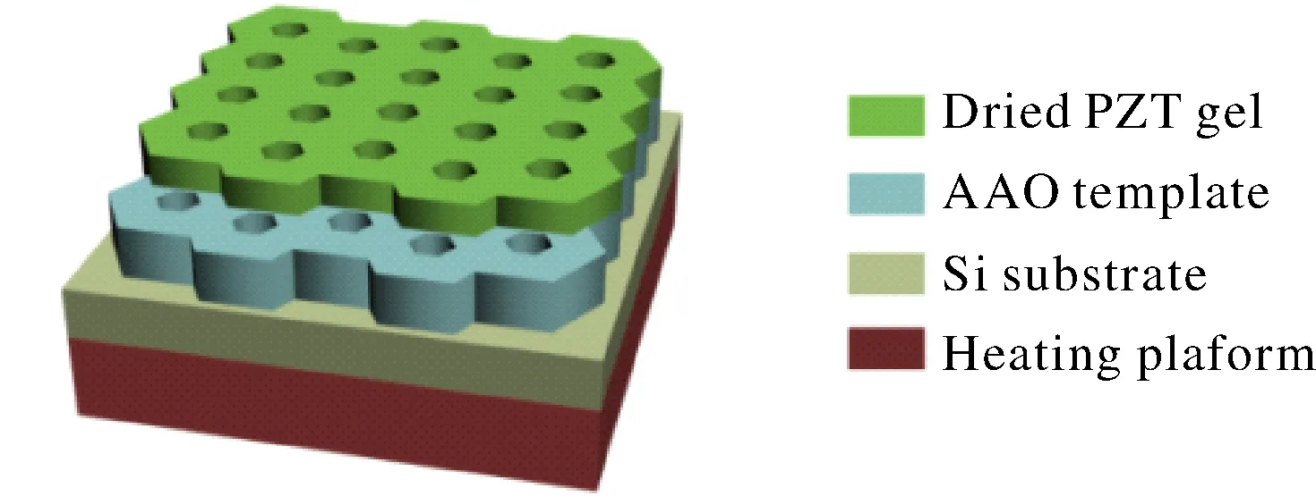
Fig.1 Stacked structure with the dried PZT gel
1.3Characterization
The morphologies of as-prepared samples were characterized by Nova Nano-SEM 450 scanning electron microscopy (Fig.2). The phase assemblage of specimens was examined by X-ray diffraction (XRD) (D8, Brucker) using Cu Ka (1.540 6 Å) radiation and a graphite monochromator in 2 h range of 10°~80°(Fig.3). EDS mapping of SEM reveals the presence of all elements of PZT (Fig.4). Transmittance measurements were performed using a UV-visible spectrophotometer (Lambda 35) (Fig.5).
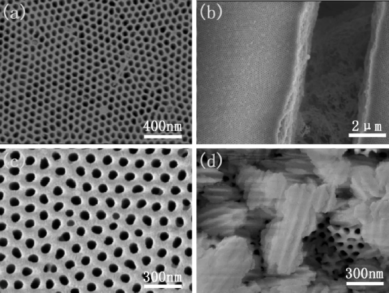
Fig.2 SEM images (a) an AAO template, (b) low magnification of PZT PCs, (c) high magnification of PZT PCs, and (d) high magnification of cracking area in Fig.2(b).
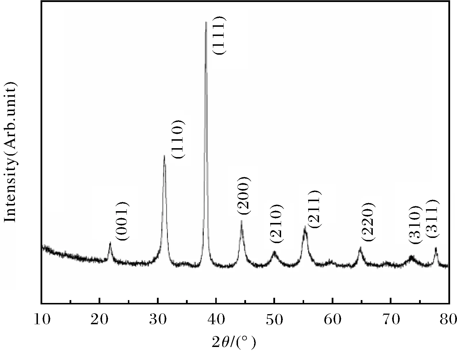
Fig.3 XRD pattern of PZT PCs
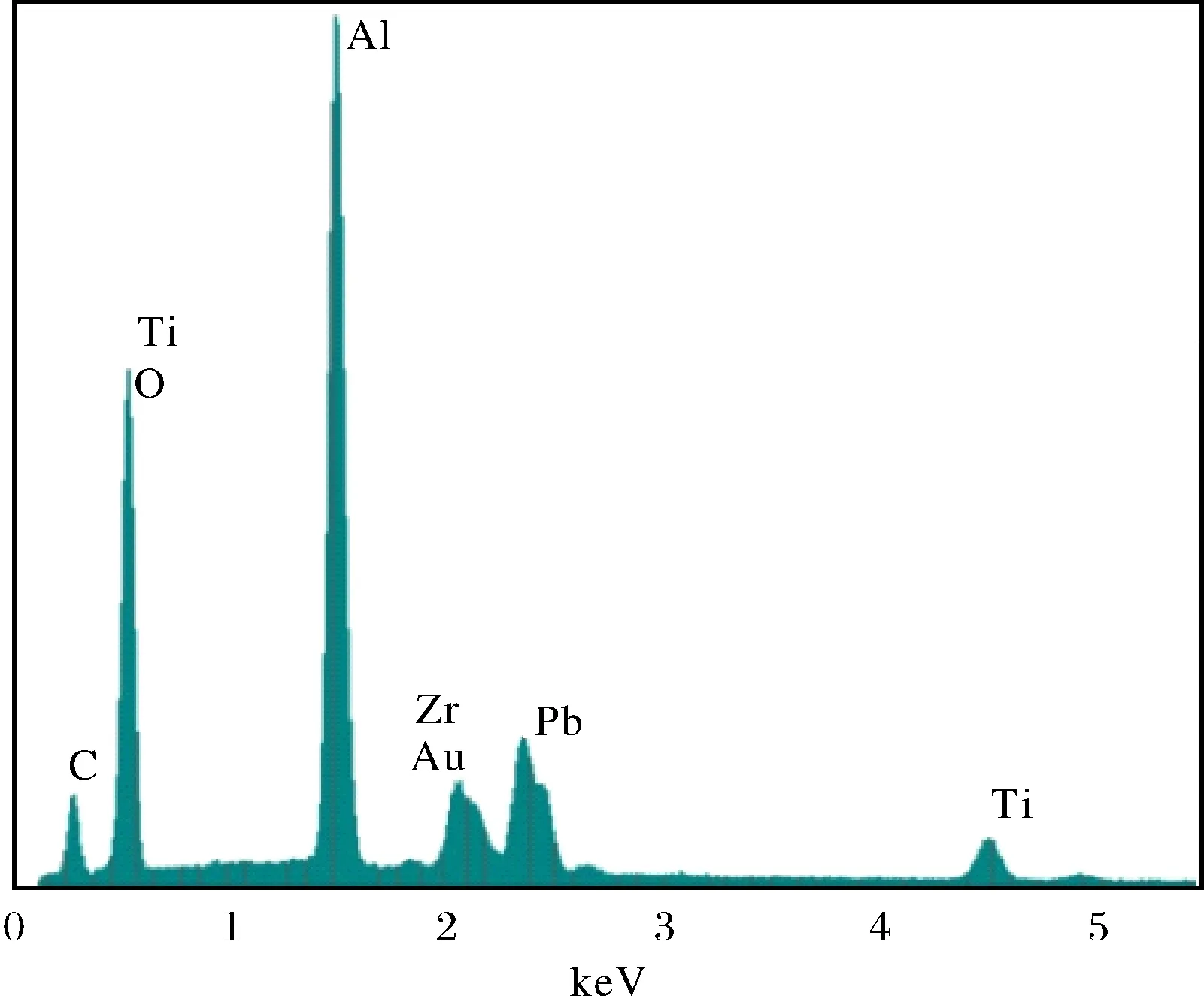
Fig.4 EDS mapping of PZT PCs
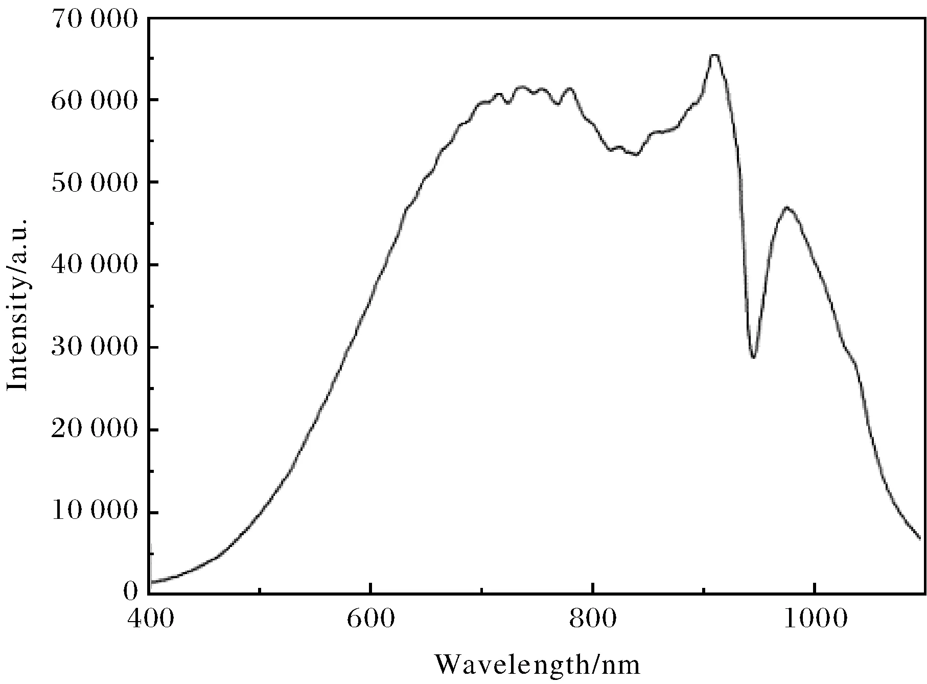
Fig.5 Transmittance spectrum of PZT PCs
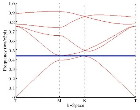
Fig.6 The band diagram for PZT PCs(with a=110 nm and r=88 nm)
2Results and discussion
PZT PCs supported on Si substrate were prepared by spin-coating of the precursor and subsequent annealing. The process resulted in characteristic PZT PCs architecture. During spin-coating, the precursor was spin-coated on the porous surface of AAO template, and the precursor did not(at least did not completely)permeate into the pore wall of AAO. Without dipping, the precursor on the AAO template was immediately transferred on the heating platform. At 60℃ the nanosized sol droplets were thermally depleted from the surface of AAO template. Due to the constant heating, major PZT gel took shape on the surface of AAO template instead of in pore channel of AAO template. When the spin-coating/heating process was repeated, the desired PZT PCs layer thickness was obtained. The annealing at 650℃ resulted in a distinguishable layer consisting of dense PZT PCs, which inherited the porous structure of AAO template. Thus, the PZT PCs layer was fabricated using the very simple and low cost sol-gel technique based on an AAO template. The SEM and all other subsequent characterization were carried out on the as-prepared substrate supported thin films without substrate removal.
SEM was employed to investigate the morphologies of the grown structures. Figure 2a is the SEM planar view of the as-prepared AAO with uniform and ordered arrays. As shown, the thickness of the PZT layer was measured to be about 1 μm and the diameter of the pores to be approximately 80 nm. Low magnification images (Fig.2b) show large area PZT PCs with cracking area. High magnification images (Fig.2c) show an interconnected PZT nanopore structure on the surface of the AAO template, and Figure 2d shows high magnification of cracking area, which is on the cracking area of the PZT PCs in Fig.2b. It can be seen that the nanostructure has spatially periodical layout and the composition is homogeneous, which confirm the 2D ordering and porosity, and this indicated the PZT PCs were successful prepared. The results show that the structure of the AAO template can support the PZT sol in the spin-coating process and dried PZT gel on heating platform.
X-ray diffraction was used to evaluate the phase and structure of the grown PCs. The annealing of the as-prepared stacked structure in turn undergone 170℃ for 10 min, 400℃ for 10 min, then 650℃ for 1 h in a Muffle furnace. Fig.3 shows the XRD pattern of the crystalline PZT PCs, which indicated the presence of tetragonal phase.
In Fig.4, EDS mapping of PZT PCs reveals the presence of all elements Pb, Zr, Ti and O of PZT. Besides, there are the Al peak from AAO, the Au peak from gold thermally evaporated before SEM checking and the C peak from organic contaminations deposited during and/or after preparation.
Fig.5 shows a sample microscopic optical transmittance spectrum of PZT PCs in the wavelength ranged from 400 nm to 1 100 nm. The transmittance spectrum shows better transmittance in the complete visible range with a valley at 980 nm, which implies that the PZT PCs show excellent optical property as an optical film and the film is highly transparent in the visible region, which matched the simulated results (Fig.6) using the Plane Wave Expansion (PWE) method.
The arrays of PZT PCs with the same geometry of AAO template (the nanopore radiusr=88 nm and a constant valuea=110 nm) was modeled using PWE method to calculate the band gaps displayed by the arrays towards the TE-mode waves incident from every direction. The calculated band diagram is shown in Fig.6. In the diagram normalized frequency (on the vertical scale) has been plotted against the incident directions into the lattice. The normalized frequencyωa/2πc, whereωis the angular frequency andcthe velocity of light in vacuum, simplifies toa/λ suggesting that the wavelength can be calculated by dividing the lattice constant a with the normalized frequency. The calculations showed that the arrays display a band gap from 970 to 990 nm (ωa/2πc=0.431-0.443). The light in this band gap can propagate in the 2D plane of PZT PCs, but the light in other band gap will be prohibited to propagate. The prohibited light will pass through the pore channel of PZT PCs, on the contrary the light in band gap from 970 to 990 nm is reflected back.
3Conclusions
In summary, we have demonstrated that the crystalline tetragonal PZT PCs with nanopore arrays were successfully fabricated utilizing a sol-gel process based on the AAO template. The obtained PCs not only show that the nanostructure has spatially periodical distribution, but also exhibit good optical transmittance properties. The advantage of this sol-gel process with AAO to fabricate FE nanopore arrays lies in its low cost and simplicity. It is worthy to note that the good performance of the transmittance is achieved without a careful optimization of the structure parameters, which indicates that there is a room to further improve the structure performance. The desired optical properties of the FE PCs can be obtained by controlling the parameters of structure, such as the refractive index of different FE materials, periodicity, and the porosity by the changing parameters of AAO template and annealing condition. This study opens a pathway for the effective fabrication and studies of FE nanopore arrays in uniquely large area, which provides a convenient and reproducible method in complex ferroelectric nanopore arrays systems. And it also has a certain role in promoting in the ferroelectric research.
Acknowledgments The authors acknowledge the financial support from National High-tech R&D Program (863 Program) of China (Grant No.2015AA043302); National Natural Science Foundation of China (Grant No. 61474048); Hubei University of science and Technology Foundation under Grant No. ky14049.
[1] SAKODA K. Optical Properties of Photonic Crystals [M]. New York: Springer Berlin Heidelberg, 2005.
[2] BUSCH K, FRANK M, GARCIA-MARTIN A, et al. A solid state theoretical approach to the optical properties of photonic crystals [J]. Physica Status Solidi (A), 2003, 197: 637-647.
[3] DENZ C, FLACH S, KIVSHAR Y S. Nonlinearities in Periodic Structures and Metamaterials [M]. New York :Springer Heidelberg Dordrecth, 2010.
[4] KIM S, GOPALAN V. Strain-tunable photonic band gap crystals [J]. Appl Phys Lett, 2001, 78: 3015-3017.
[5] YAMAMOTO N, NODA S, SASAKI A, et al. New realization method for Three-Dimensional photonic crystal in the optical wavelength region: Experimental consideration [J]. Jpn J Appl Phys, 1997, 36: 1907.
[6] JUDITH E G, WIJNHOVEN J, WILLEM L V. Preparation of photonic crystals made of air spheres in Titania [J]. Science 1998, 281: 802.
[7] LINES M E, GLASS A M, Principles and Applications of Ferroelectrics and Related Materials [M]. Oxford:Clarendon Press, 2004.
[8] FERRARO P, GRILLI S, NATALE P D. Ferroelectric Crystals for Photonic Applications: Including Nanoscale Fabrication and Characterization Techniques [M]. Berlin:Springer, 2009.
[9] BOYD R W. Nonlinear Optics[M]. Oxford:Academic Press, 2008.
[10] SOTEN I, MIGUEZ H, YANG S M, et al. Barium titanate inverted opals—Synthesis, characterization, and optical properties [J]. Adv Funct Mater, 2002, 12: 71-77.
[11] GALLORO J, GINZBURG M, MIGUEZ H, et al. Replicating the structure of a crosslinked polyferrocenylsilane inverse opal in the form of a magnetic ceramic [J]. Adv Funct Mater, 2002, 12: 382-388.
[12] ZHANG W, HAN P, LAN A, et al. Defect modes tuning of one-dimensional photonic crystals with lithium niobate and silver material defect [J], Physica E, 2012, 44: 813-815.
[13] JUNG W S, LEE W H, JU B K, et al. Enhanced output power of PZT nanogenerator by controlling surface morphology of electrode [M]. J Nanosci Nanotechno, 2015, 15: 8907-8911.
[14] HE G, ZHOU Y J, PENG C. Dielectric and ferroelectric performance of Pb (Zr(x)Ti(1-x))O3thin films with compositional gradients [J]. J Nanosci Nanotechno, 2015, 15: 7099-7103.
[15] ZHANG Q, CORKOVIC S, SHAW C, et al. Effect of porosity on the ferroelectric properties of sol-gel prepared lead zirconate titanate thin films [J]. Thin Solid Films, 2005, 488: 258.
[16] JUNG W, DO Y, KANG M, et al. Energy harvester using PZT nanotubes fabricated by template-assisted method [J]. Curr Appl Phys, 2013, 13: S131-S134.
[17] GONG S S, TANG Y W, XU L, et al. Preparation and characterization of the MWNTs/PAA composites [J] . Journal of Huazhong Normal University(Nat.Sci.), 2008, 42: 77-80.
[18] LEE W, PARK S J. Porous anodic aluminum oxide: anodization and templated synthesis of functional nanostructures [J]. Chem Rev, 2014, 114: 7487-7556.
[19] SUN T Y, XU Z M, ZHAO W N, et al. Fabrication of the similar porous alumina silicon template for soft UV nanoimprint lithography [J]. Appl Surf Sci, 2013, 276: 363-368.
[20] SUN T Y, XU Z M, WU X H, et al. Porous light-emitting diodes with patterned sapphire substrates realized by high-voltage self-growth and soft UV nanoimprint processes [J]. J Lightwave Technol, 2013, 32: 326-332.
[21] YI G, SAYER M. An acetic acid/water based sol-gel PZT process I: Modification of Zr and Ti alkoxides with acetic acid [J]. J Sol-gel Sci Techn, 1996, 6: 65-74.
[22] YI G, SAYER M. An acetic acid/water based sol-gel PZT process II: formation of a water based solution [J]. J Sol-gel Sci Techn, 1996, 6: 75-82.
2016-08-18.
“863”计划资助项目(2015AA043302);国家自然科学基金项目(61474084);湖北科技学院校级项目(Ky14049).
1000-1190(2017)01-0062-05
溶胶凝胶法制备锆钛酸铅纳米孔状光子晶体阵列
李泽平1,2, 熊 钢1*, 梅丽红1, 王 耿1, 屈小鹏2
(1.湖北科技学院 电子与信息工程学院, 湖北 咸宁 437005; 2.华中科技大学 光学与电子信息学院, 武汉 430074)
基于阳极氧化铝模板,使用旋涂法制备了锆钛酸铅纳米孔状光子晶体阵列.利用扫描电子显微镜、X射线衍射仪和能谱仪表征了其结构,形态和尺寸分布.结果显示制备的锆钛酸铅光子晶体呈正方晶相,尺寸统一,分布均匀,同时展现了良好的光学透射特性.这个简单,低成本又可行的制备方法为制备铁电纳米孔阵列结构提供了一条方便又可复制的途径.
锆钛酸铅纳米孔状光子晶体; 阳极氧化铝; 溶胶凝胶法; 旋涂; 透射
O614.41
A
*通讯联系人. E-mail: 942749725@qq.com.
