On the role of piezoelectricity in phonon properties and thermal conductivity of GaN nanofilms
2017-01-06LinliZhuHaonanLuo
Linli Zhu,Haonan Luo
Department of Engineering Mechanics and Key Laboratory of Soft Machines and Smart Devices of Zhejiang Province,Zhejiang University,Hangzhou 310027,China
On the role of piezoelectricity in phonon properties and thermal conductivity of GaN nanofilms
Linli Zhu∗,Haonan Luo
Department of Engineering Mechanics and Key Laboratory of Soft Machines and Smart Devices of Zhejiang Province,Zhejiang University,Hangzhou 310027,China
H I G H L I G H T S
·The impact of piezoelectricity on the phonon properties and thermal conductivity of gallium nitride(GaN)nanofilms is studied theoretically.
·The elastic model combining with the piezoelectric constitutive relation is applied to describe the confined-phonon properties.
·The piezoelectric effect leads to the change of the temperature-and size-dependence of thermal conductivity.
A R T I C L E I N F O
Article history:
Received 28 September 2016
Received in revised form
1 November 2016
Accepted 1 November 2016
Available online 11 November 2016
GaN nanofilm
Phonon properties
Elastic model
Piezoelectricity
Phonon thermal conductivity
The effect of piezoelectricity on phonon properties and thermal conductivity of gallium nitride(GaN) nanofilms is theoretically investigated.The elasticity model is utilized to derive the phonon properties in spatially confined GaN nanofilms.The piezoelectric constitutive relation in GaN nanofilms is taken into account in calculating the phonon dispersion relation.The modified phonon group velocity and phonon density of state as well as the phonon thermal conductivity are also obtained due to the contribution of piezoelectricity.Theoretical results show that the piezoelectricity in GaN nanofilms can change significantly the phonon properties such as the phonon group velocity and density of states, resulting in the variation of the phonon thermal conductivity of GaN nanofilms remarkably.Moreover, the piezoelectricity of GaN can modify the dependence of thermal conductivity on the geometrical size and temperature.These results can be useful in modeling the thermal performance in the active region of GaN-based electronic devices.
©2016 The Authors.Published by Elsevier Ltd on behalf of The Chinese Society of Theoretical and Applied Mechanics.This is an open access article under the CC BY-NC-ND license(http:// creativecommons.org/licenses/by-nc-nd/4.0/).
Gallium nitride(GaN),as one of the wurtzite nitride semiconductors,has been regarded as the state of the art materials for the next generation of high-power optoelectronics devices and ultrapower switches[1,2].It is because that the wurtzite nitride semiconductors(GaN,AlN,InN)possess the electrical,optical,and thermal properties at high temperatures[3,4].Thermal properties of GaN play an important role in the applications of optoelectronic/microelectronic devices due to that the self-heating in the active regions strongly influences the performance and reliability of the devices.Experiments proved that the piezoelectric effects can significantly affect the performance of micro/nanoelectronic devicessuchastheefficiencydroopinwurtzitenitride-basedlightemitting diodes(LEDs)[5].Consequently,the accurate value of the thermaltransportpropertyofGaNnanostructuresbecomesimportantindesigningtheGaN-basedelectronicdevicesandkeepingthe performance of corresponding devices reliable.
Since the heat in semiconductors is,in principle,transported by phonons,it becomes essential to investigate the phonon properties and phonon thermal conductivity in semiconductor nanostructures[6,7].A few groups have studied the phonon thermal conductivity of GaN in the bulk and nanostructure forms both in experiment and in theory.Sichel and Pankove[8]firstly measured the thermal conductivity of GaN film,and Guthy et al.[9]obtained the thermal conductivity of the GaN nanowires with different diameters from 97 to 181 nm in experiment.Theoretically,Slack[10]predicted the bulk thermal conductivity of GaN as 170 W/(m·K)at room temperature.Al-Shaikhi et al.[11]applied the Callaway’s relaxation-time theory to achieve the thermal conductivity of GaN bulks and films.Moreover,the Boltzmann transport equation approach was also adopted to calculate the thermal conductivity of GaN nanowires and GaN nanotubes[12,13],and the atomic method are also often carried out to simulate the thermal conductivity of GaN bulks and GaN nanostructures[11,14,15].However,these studies have not accounted for the influence of the piezoelectricity on the thermal conductivity of GaN materials. Even though Sahoo studied the effects of piezoelectric polarization and macroscopic polarization on phonon group velocity and thermal conductivity of bulk nitride wurtzites[16,17],the study of the piezoelectric effect on the phonon properties and thermal conductivity in spatially confined GaN nanofilms is still in lack.
In this letter,the phonon properties and thermal conductivities of wurtzite–GaN nanofilm accounting for the piezoelectric effect aresimulatedtheoretically.Weapplytheelasticmodeltocalculate the phonon properties such as the phonon group velocity and phonon density of state in spatially confined GaN nanofilms.The influenceofpiezoelectricityistakenintoaccountincalculatingthe phonon properties and thermal conductivity through combining the piezoelectric constitutive relation in elastic model.Theoretical results show that the piezoelectricity in GaN nanofilms can change the phonon velocity and density of state of GaN nanostructures significantly,resulting in the modification of the phonon thermal conductivity in GaN nanofilms.
The elasticity model has been always used to calculate the acoustic phonon properties of spatially confined nanostructures since the particle motion in the crystals can be well described by vibration equation[18–20].So,we can begin from the vibration equations based on the elasticity theory as

whereuiis the particle displacement vector,i,j,k,l=1,2,3 are the indices of the three Cartesian coordinate axes.ρis the density of the natural state,σijis the stress tensor.Due to the piezoelectric effect,thestress–strainrelationshipinvolvesthecouplingbetween the elastic strain and electric field,given by

whereeijkis the third rank piezoelectric tensor,Ekis the electric field tensor andCijklis the four-order modulus tensor.As a result, the vibration equation can be rewritten as
For isotropic materials,the elastic modulus tensor only depends on the elastic constantsC11andC44.Here,we use the general rules to contract the indices:(iijj)→ (ij),and(12)→ (6),(13)→(5),(23)→ (4).Moreover,the constitutive relation between the electric displacement and the elastic strain can be presented as

whereDiis the electric displacement,εijis the dielectric tensor. From the Maxwell equation,we also have the relation∇·D=ρ0, whereρ0is the density of free charges.Then,according to Eq.(3), we have

Due to theρ0small enough for GaN,it can be safe to assume that∇·D≈0[16].
Suppose that thex3direction is the transverse direction of the thickness of the GaN nanofilm,andx1andx2are the in-plane directions of the film.The acoustic waves propagate along thex1direction when the heat energy is along thex1direction.Thereby, the displacements of the nanofilm in Eq.(3)are the functions ofx1andx3in the form of

whereωis the frequency andqis the wave vector.¯u(x3)is the amplitude of displacement vector andiis imaginary unit.The solution of electric field can also follow the form of

The boundary conditions can be written as

Then,the phonon dispersion relations of GaN nanofilm can be calculated numerically based on the eigenvalue equation with the boundary conductions.Once the phonon dispersion relations are obtained for the nanofilms,the phonon frequency can be determined by using the finite difference method.From the determined vibrational spectrum of nanofilm,the phonon group velocity of various modes can be written as[12]

where the subscriptnis the quantum number of the modes.With a given polarization,nis equal to the ratioa/(2˜a).Here,˜ais the lattice constant.The quasi-2D phonon density of state is given by[12]

Owingtothatpiezoelectricityeffectcanchangethephonondispersion relations for different modes,the phonon group velocity and density of state are dependent on the property of piezoelectricity. The thermal performance of semiconductor nanostructures, in principle,is relevant to the phonon properties such as the phonon group velocity and the phonon density of states.When the phonon properties are determined for the GaN nanofilm with accounting for the piezoelectricity effect,the in-plane phonon thermal conductivity of nanofilm can be reached from[21]


In order to explore the influence of piezoelectric on phonon properties and thermal performance,we simulate the phonon group velocity,phonon density of state,and the phonon thermal conductivity of wurtzite–GaN nanofilms.The material parameters related to the phonon scattering rates are taken from the literatures[8,12].The bulk elastic parametersCijklandCijklmnof wurtzite–GaN areC11=293 GPa,C12=159 GPa,C44=155 GPa,C111= -1213 GPa,C112= -867 GPa,C123= -253 GPa,C144=-46 GPa,andC155=-606 GPa[22,23],and the dielectric parameters areε11=ε22=9.5,ε33=12[16].
Figure 1(a)shows the phonon group velocity of GaN nanofilm varying with the phonon energy under different piezoelectric constants,in which the nanofilm thickness is adopted as 5 nm. It is clearly noted that the phonon average group velocity in GaN nanofilm is significantly sensitive to the piezoelectric constant. When we do not consider the piezoelectric effect,the value of the phonon average group velocity arrives at 4500 m/s in the region of the phonon energy is close to zero,which refers to the Brillouin zone.While the piezoelectric constant of GaN nanofilm turns into 7 C/m2,the phonon average group velocity dramatically increases from 4500 to 5000 m/s.It has been demonstrated in Ref.[16]that the piezoelectricity leads to the increment of the average group velocity around one percentage for Bulk GaN.Since the piezoelectric constant of GaN nanofilm is greater than the one of bulk counterpart,the change of group velocity in GaN nanofilm is more significant than that in bulk GaN with considering the piezoelectric effect.When the piezoelectric constant is changed as 3 C/m2,theinfluence ofpiezoelectriceffect onthephononaverage group velocity becomes weaker.Figure 1(b)depicts the variation of the phonon average group velocity with phonon energy with different piezoelectric constants for the nanofilm thickness of 7 nm.Comparing with GaN nanofilm thickness of 5 nm,the piezoelectric effect also significantly changes the phonon average group velocity and the increment of velocity is greater than that in the former case.Similarly,Fig.1(c)plots the variation of the phonon average group velocity for the GaN nanofilm with the thickness of 12 nm.Owing to the increase of nanofilm thickness, the number of the phonon modes improves rapidly and the oscillation frequency of the phonon average group velocity is also enhanced dramatically.One also can find in Fig.1(c)that the wave peaks of the phonon average group velocity emerge more frequently in the region of higher energy.In addition,the piezoelectric effect also distinctly changes the phonon average group velocity.
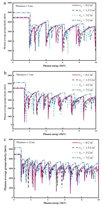
Fig.1. Phonon average group velocity vs.phonon energy with different piezoelectric constants for GaN nanofilm with the thickness of(a)5 nm,(b)7 nm, and(c)12 nm.
Figure 2(a)shows the variation of the phonon density of states (DOSs)with phonon energy for GaN nanofilm with 5 nm thickness. It is clearly observed that the DOS rises step-by-step with the increment of phonon energy and then decreases step by step when the curve reaches the peak.The piezoelectric effect significantly changes the distribution of DOS vs.phonon energy with two features.On the one hand,it makes the DOS distributing around more extensive energy region and the maximum value can reach 50 MeV.It is because of the fact that the piezoelectricity can increase the phonon energy of GaN nanofilm.On the other hand, the peak of the DOS is modified obviously.The maximum value of DOSdecreasesfrom3.5×1014to2.0×1014s/m3,whichisresulting from the fact that the piezoelectric effect improves the energy difference between the adjacent modes.Figure 2(b)depicts the variation of the phonon DOS with different piezoelectric constants for GaN nanofilm with the thickness of 7 nm.It is clear to find that the peak values of phonon DOS reaches 4.0× 10¹⁴s/m3which is higher than that of GaN nanofilm with 5 nm thickness. Withconsideringthepiezoelectriceffect,theDOSdistributesalong more extensive energy regions and its peak value drops more dramatically.Figure 2(c)further shows the variation of the phonon DOS for GaN nanofilm with the thickness of 12 nm.Comparing with the thinner films,the steps in curves of 12 nm GaN nanofilmmanifests more smoothly.This is due to that thickening the nanofilm leas to the number of phonon modes increasing.

Fig.2.Phonon density of state vs.phonon energy with different piezoelectric constants for GaN nanofilm with the thickness of(a)5 nm,(b)7 nm,and(c)12 nm.
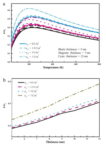
Fig.3.(Color online)(a)Phonon thermal conductivity vs.temperature for different nanofilm thickness and different piezoelectric constants of GaN nanofilm,and (b)thesize-dependentphononthermalconductivityofGaNnanofilmwithdifferent piezoelectric constants.κ0is the bulk phonon thermal conductivity of GaN.
Figure 3(a)plots the phonon thermal conductivity varying with the temperature for different nanofilm thickness and different piezoelectric constants of GaN nanofilm.It is noticed from Fig.3(a) that the increase of piezoelectric constant improves obviously the phonon thermal conductivity of GaN nanofilm.With the small piezoelectric constants such as 1.5 C/m2or 3 C/m2close to the piezoelectric constants of the bulk GaN,the influence of piezoelectricity on phonon thermal conductivity is not significant. When the film thickness decreases to the nanometer scale, the piezoelectric constant is increased due to the size effect. For example,with the piezoelectric constant as 7 C/m2,the piezoelectric effect significantly improves the phonon thermal conductivity of GaN nanofilm and the conductivity has increased by~20%when the temperature is between 200 and 300 K.This is in accord with the simulated results for bulk InN[17]qualitatively. Figure 3(b)depicts the variation of phonon thermal conductivity with film thickness for GaN nanofilm with different piezoelectric constants.From the figure,one can note that the phonon thermal conductivity displays the size effect which is stemmed from the quantum confinement effect,indicating that the phonon thermal conductivityincreaseswiththeincrementofthethickness.Besides that,the influence of the piezoelectricity on the phonon thermal conductivity meets a linear relationship and the phonon thermal conductivity is proportional to the piezoelectric constant.
In summary,we studied the piezoelectric effect on the phonon properties and thermal performance of GaN nanofilms theoretically.The influences of piezoelectricity on the phonon group velocity,phonon density of states,and phonon thermal conductivity of GaN nanofilms are quantitatively explored.The simulation results demonstrated that the piezoelectric effect in GaN nanofilms can notably change the phonon properties and the phonon thermal conductivity.Moreover,the piezoelectricity property can also modify the temperature and size-dependence of phonon thermal conductivity in GaN nanofilm.The results in this work will be helpful for controlling the thermal performance in GaN-based nanoelectronic devices.
Acknowledgments
The authors gratefully acknowledge the support received from the National Natural Science Foundation of China(11472243, 11302189,11321202)and the Doctoral Fund of Ministry of Education of China(20130101120175).
[1]K.Chung,C.H.Lee,G.C.Yi,Transferable GaN layers grown on ZnO-coated graphene layers for optoelectronic devices,Science 330(2010) 655–657.
[2]M.Nazari,B.L.Hancock,E.L.Piner,et al.,Self-heating profile in an AlGaN/GaN heterojunction field-effect transistor studied by ultraviolet and visible micro-Raman spectroscopy,IEEE Trans.Electron Devices 62(2015) 1467–1472.
[3]Y.Huang,X.Duan,Y.Cui,et al.,Gallium nitride nanowire nanodevices,Nano Lett.2(2002)101–104.
[4]S.Gradečak,F.Qian,Y.Li,et al.,GaN nanowire lasers with low lasing thresholds,Appl.Phys.Lett.87(2005)173111.
[5]Y.K.Kuo,M.C.Tsai,S.H.Yen,et al.,Effect of P-type last barrier on efficiency droop of blue ingan light-emitting diodes,IEEE J.Quantum Electron.46(2010) 1214–1220.
[6]Z.P.Xu,Heat transport in low-dimensional materials:A review and perspective,Theor.Appl.Mech.Lett.6(2016)113–121.
[7]Y.H.Yu,Y.Y.Gao,J.Z.Song,Recent advances on thermal analysis of stretchable electronics,Theor.Appl.Mech.Lett.6(2016)32–37.
[8]E.K.Sichel,J.I.Pankove,Thermal conductivity of GaN,25-360K,J.Phys.Chem. Solids 38(1977)330.
[9]C.Guthy,C.Y.Nam,J.E.Fischer,Unusually low thermal conductivity of gallium nitride nanowires,J.Appl.Phys.103(2008)064319.
[10]G.A.Slack,Nonmetallic crystals with high thermal conductivity,J.Phys.Chem. Solids 34(1973)321–335.
[11]A.AlShaikhi,S.Barman,G.P.Srivastava,Theory of the lattice thermal conductivity in bulk and films of GaN,Phys.Rev.B 81(2010)195320.
[12]J.Zou,Lattice thermal conductivity of freestanding gallium nitride nanowires, J.Appl.Phys.108(2010)034324.
[13]G.Zhou,L.L.Li,Phonon thermal conductivity of GaN nanotubes,J.Appl.Phys. 112(2012)014317.
[14]K.Jung,M.Cho,M.Zhou,Thermalandmechanicalresponseof[0001]-oriented GaN nanowires during tensile loading and unloading,J.Appl.Phys.112(2012) 083522.
[15]L.Lindsay,D.A.Broido,T.L.Reinecke,Thermal conductivity and large isotope effect in GaN from first principles,Phys.Rev.Lett.109(2012)095901.
[16]B.K.Sahoo,Effect of piezoelectric polarization on phonon group velocity in nitride wurtzites,J.Mater.Sci.47(2012)2624–2629.
[17]B.K.Sahoo,Effect of macroscopic polarization on thermal conductivity of InN, J.Alloys Compd.603(2014)217–221.
[18]A.Balandin,K.L.Wang,Significant decrease of the lattice thermal conductivity due to phonon confinement in a free-standing semiconductor quantum well, Phys.Rev.B 58(1998)1544–1549.
[19]L.L.Zhu,H.H.Ruan,Influence of prestress fields on ther phonon thermal conductivity of GaN nanostructures,ASME J.Heat Transfer 36(2014)102402.
[20]L.L.Zhu,H.N.Luo,Phonon properties and thermal conductivity of GaN nanofilm under prestress and surface/interface stress,J.Alloys Compd.685 (2016)619–625.
[21]P.Martin,Z.Aksamija,E.Pop,et al.,Impact of phonon-surface roughness scattering on thermal conductivity of thin Si nanowires,Phys.Rev.Lett.102 (2009)125503.
[22]S.P.Łepkowski,J.A.Majewski,G.Jurczak,Nonlinear elasticity in III-N compounds:Ab initio calculations,Phys.Rev.B 72(2005)245201.
[23]S.P.Łepkowski,I.Gorczyca,Ab initio study of elastic constants in InxGa1-xN and InxAl1-xN wurtzite alloys,Phys.Rev.B 83(2011)203201.
∗Correspondence to:Department of Engineering Mechanical,Zhejiang University,Hangzhou 310027,China.
E-mail address:llzhu@zju.edu.cn(L.Zhu).
http://dx.doi.org/10.1016/j.taml.2016.11.001
2095-0349/©2016 The Authors.Published by Elsevier Ltd on behalf of The Chinese Society of Theoretical and Applied Mechanics.This is an open access article under the CC BY-NC-ND license(http://creativecommons.org/licenses/by-nc-nd/4.0/).
*This article belongs to the Solid Mechanics
杂志排行
Theoretical & Applied Mechanics Letters的其它文章
- Synergy to discovery and innovation—Growth of nanorods
- Buckling and post-buckling analyses of size-dependent piezoelectric nanoplates
- Numerical simulation of domain switching in multilayer ferroelectric actuators
- Coriolis effect on responses of rotating thin piezoelectric hollow cylinder
- On transition of type V interaction in double-wedge flow with non-equilibrium effects
- Numerical simulation of Gurney flap on SFYT15thick airfoil