Numerical simulation of domain switching in multilayer ferroelectric actuators
2017-01-06QunLi
Qun Li
State Key Laboratory for Strength and Vibration of Mechanical Structures,School of Aerospace,Xi’an Jiaotong University,Xi’an 710049,China
Letter
Numerical simulation of domain switching in multilayer ferroelectric actuators
Qun Li
State Key Laboratory for Strength and Vibration of Mechanical Structures,School of Aerospace,Xi’an Jiaotong University,Xi’an 710049,China
H I G H L I G H T S
·Domain switching is simulated in multilayer ferroelectric actuators.
·Electromechanical behaviors ahead of the crack tip are numerically simulated.
·The size of switching zone reaches the scale of crack length.
A R T I C L E I N F O
Article history:
Received 19 September 2016
Received in revised form
31 October 2016
Accepted 1 November 2016
Available online 18 November 2016
Domain switching
Crack
Electrode
Multilayer ferroelectric actuator
Micromechanical finite element methods are developed based on a nonlinear constitutive model of ferroelectric polycrystals.Electromechanical behaviors ahead of an internal electrode tip are numerically simulated in multilayer ferroelectric actuators.Around the electrode edge,the nonuniform electric field generates a concentration of stress due to the incompatible strain as well as spontaneous strain.The preferred domain switching enhances the concentration of residual stress and may cause the actuators to crack.An electrically permeable crack emanating from an internal electrode is analyzed.A large scale domain switching zone is found in the vicinity of crack tips.The larger the actuating strain and electric field are,the larger the switching zone will be.The size of switching zone even reaches the scale of crack length with increasing electromechanical loading.
©2016 The Author(s).Published by Elsevier Ltd on behalf of The Chinese Society of Theoretical and Applied Mechanics.This is an open access article under the CC BY-NC-ND license(http:// creativecommons.org/licenses/by-nc-nd/4.0/).
Multilayer ferroelectrics have been accepted for numerous applications in smart structures and adaptive technologies as the excellent actuators in view of their small volumes,quick response, and large generated forces[1,2].A typical multilayer actuator consists of a few thin ferroelectric layers laminated one by one. A thin metallic electrode layer is embedded at the interface of two ferroelectric materials.This configuration has the advantage of achieving the enhanced electromechanical coupling properties and large drive force at low voltage.
However,the reliability of multilayer actuators is limited due to stress concentration near the electrode edge.Experiments have demonstrated that an actuator can crack around its internal electrode edges when the ceramic has a large actuating strain[3, 4],as shown in Fig.1[5].Electromechanical behaviors near theinternal electrode tip have received considerable attention in the past several years[6–8].Yang and Suo[6]analyzed the cracking in ceramic actuators caused by electrostriction by a theoretical approach and concluded that the electric field induces electrostrictive stress which drive the crack.Shindo et al.[7]discussed a nonlinear behavior induced by localized polarization switching and compared their numerical results with experimental observations.Jeong and Beom[8]researched the cracking near the edge of an internal electrode by modeling of domain switching based on the nonlinear electric theory.Zhao et al.[9]investigated the deformation and stress concentrations around the electrode tip in two multilayer actuator designs, partially and fully cofired by means of experimental measurement and numerical simulations.Most of the previous research focused on situations where linear constitutive model prevails in the bulk of ceramics and the small scale domain switching saturation condition near the electrode tip(see,the recent review articles by Zhang et al.[10],Chen and Lu[11],Kuna[12,13],among many others).
Actually,ferroelectric polycrystals consist of a threefold hierarchical microstructure.That is,the polycrystalline ceramic is composed ofgrains,and each grain is subdivided intodomains,where each domain is a collection ofunit cellsall having the same electrical dipole orientation[14–19].A nonlinear micromechanical model of ferroelectrics was developed by Huber et al.[16],where each grain comprises a set of distinct domain variants with theirown volume fractions as shown in Fig.2.Within each grain the switching event,which converts one domain variant into another, gives rise to a progressive change in remanent strain and polarization and to a corresponding change in volume fraction.In the present study,a finite element algorithm is developed for a tetragonalferroelectricsbasedonthenonlinearconstitutivelawofHuber etal.[16].Electromechanicalfieldconcentrationneartheelectrode edgeisinvestigatedinmultilayeractuators.Thesizeandconfigurationofdomainswitchingzonenearanelectricallypermeablecrack emanating from an internal electrode are numerically simulated.
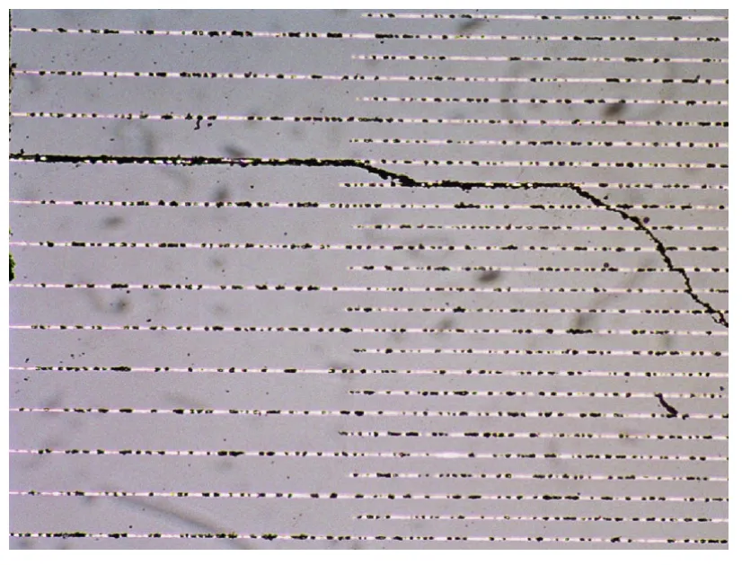
Fig.1.Experimental observation of a crack emanating from an internal electrode finally damaging the multilayer ferroelectric actuators[5].
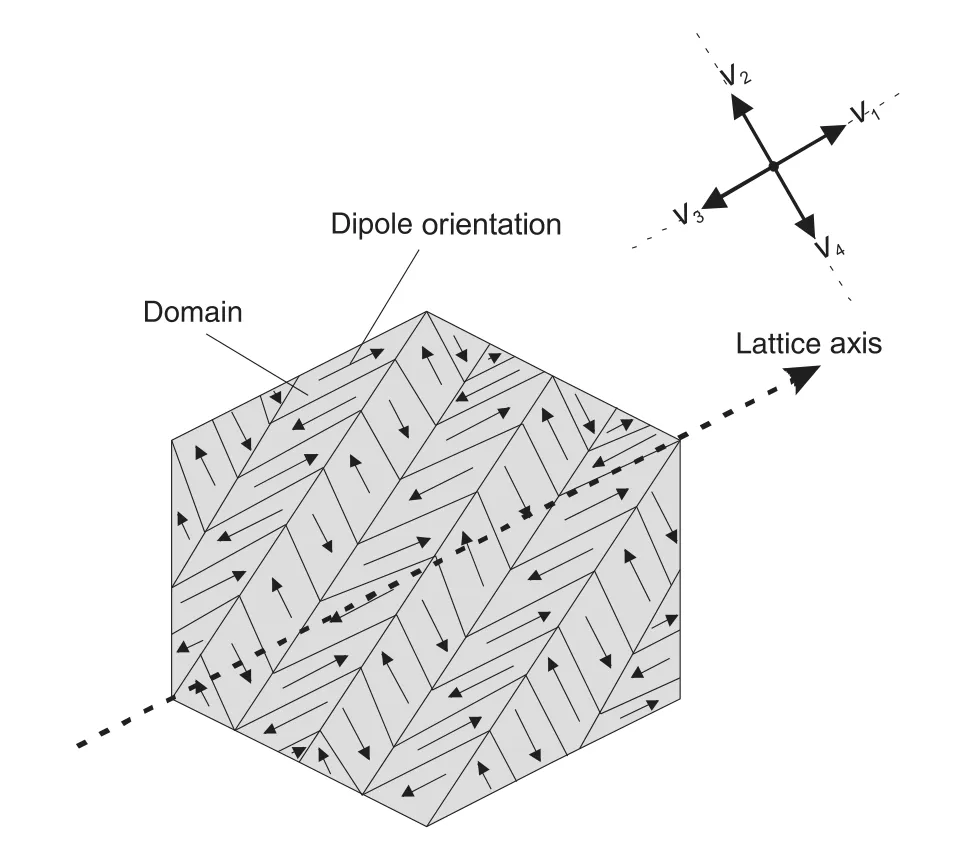
Fig.2.Schematic of one grain with its uniform lattice axis.Each grain is subdivided into domains with their own volume fractions.
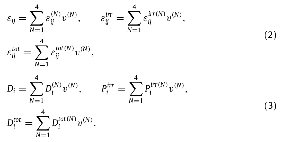
Domain wall motion within each ferroelectric crystal leads to a non-linear constitutive behavior due to the change in the spontaneous strain and polarization.The total strainand the total electric displacementare the summation of the reversible(linearεijandDi)and spontaneous(nonlinearandcomponents.The ferroelectric material behavior is described as

whereσijandEkare the stresses and the electric field components;cijkl,ekij,andκikaretheelastic,piezoelectricanddielectricconstants of the material,respectively.
Assume all considerations are restricted to thex1–x2plane, there are four allowable polarization directions for a tetragonal crystal.A domain can switch 90°clock-or anti-clockwise or it can switch 180°.Based on the micro crystalline model,it is assumed that every domain type corresponds to a volume fraction ofv(N)(N=1,2,3,4).Thus,both the linear and spontaneous parts of the strain and the electric displacement are given by the volume averages over the crystal.
Moreover,polarization domain switching relies on the balance between energy release and energy dissipation in domain.Energy dissipation is responsible for switching barriers such as the critical energy release density to switch a crystallite.The total differential of the internal energy density for nonlinear ferroelectrics can be formulated as:
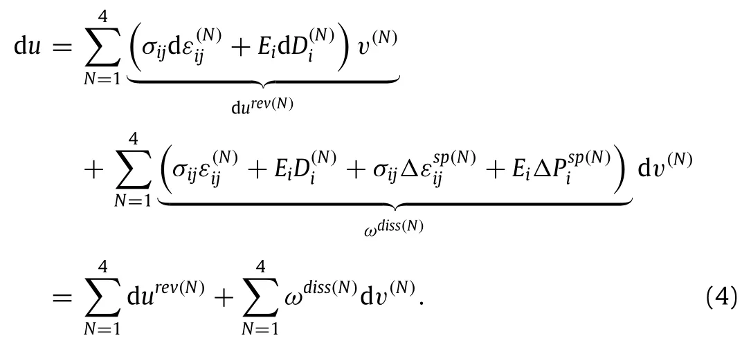
The FEM procedure should provide an updated level of the variant volume fractions when domain switching criterion(4)is reached.The evolution for the incremental volume fraction dv(N)depends on the ratio of the dissipative work and the threshold value

where dv0denotes the initial increment of volume fraction.
A finite element algorithm is developed based on the above micromechanical model.In finite element method(FEM)simulation, aGaussintegrationpointineachelementisrepresentativeofgrain withdifferentlatticeorientationandcomprisesasetofdistinctdomain variants.The finite element algorithm can be obtained by the generalized principle of virtual work.Without further elaboration the resulting variational principle may be stated in matrix notations as[19]
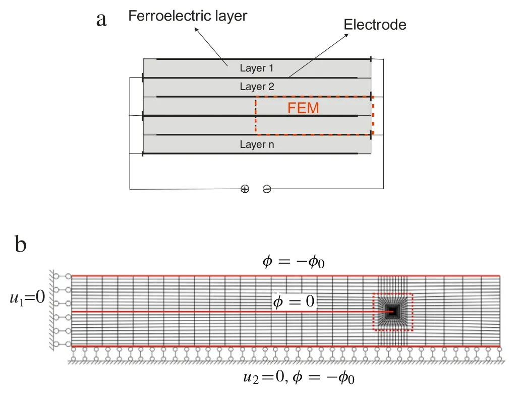
Fig.3.(a)Schematic of ferroelectric multilayer actuator and(b)FEM mesh region of specimen and boundary condition.
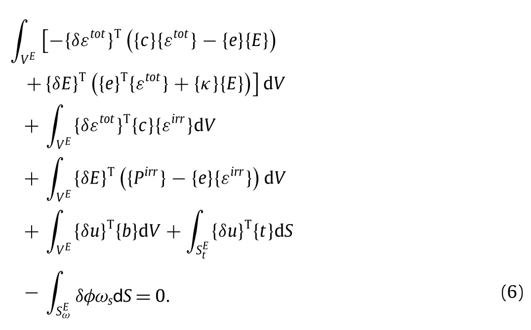
Equation(6)can be discretized in the usual manner of a finite elementformulation,i.e.,themechanicaldisplacementandelectric potential are expressed in terms of nodal values via interpolation functions{Nu}and{Nφ}.The discretized result is the algebraic equation system

where{u}and{φ}are the nodal values of the mechanical displacement and electric potential,respectively. is the elastic stiffness matrix.

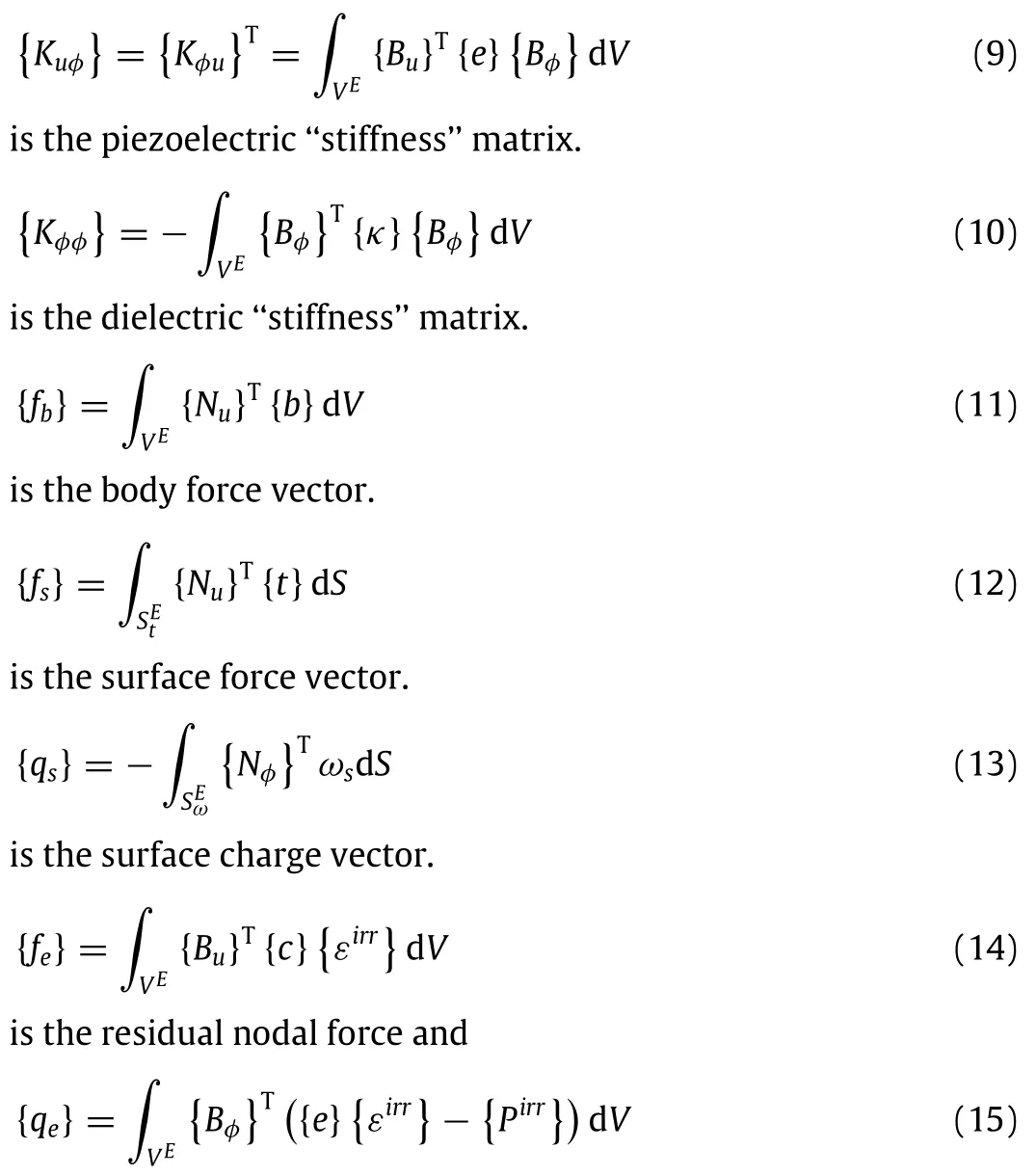
is the residual nodal charge resulting from irreversible domain switching.In Eqs.(8)–(15),the matrices{Bu}and{Bφ}give the differential relation between nodal variables{u}and{φ}and strains and electric fields,respectively.
This part is concerned with domain switching near the electrode tip in multilayer actuators.Owing to their symmetry,it is more representative and more efficient to analyze only half of two individual layers in Fig.3(a).A sample model with the size of 6×1 mm with the length of electrode 4.5 mm is shown in Fig.3(b). The FE mesh consists of 1530 isoparametric quadratic 8-node elements with the refined area around the electrode tip.To avoid rigid body motion,the left edge of the specimen is constrained along thex1direction,while the bottom edge is constrained alongx2.The electric field is applied by prescribing a potential difference between the top/bottom surfaces and electrode surface in specimen.Atypicallytetragonal BaTiO3is analyzedinnumerical computations.
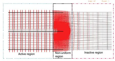
Fig.4.Schematic representation of electric field vectors near the electrode tip.
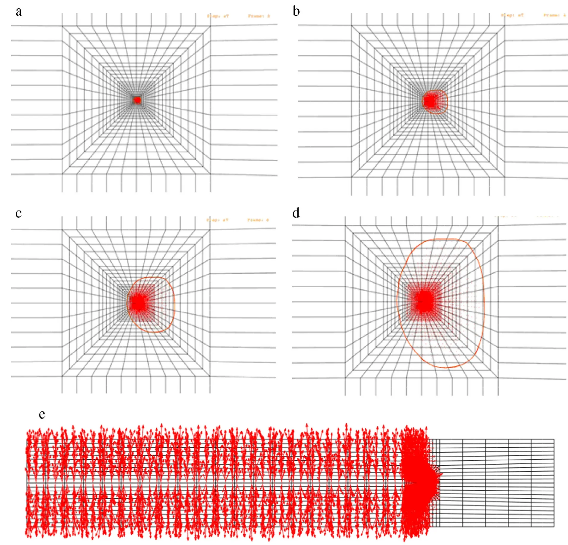
Fig.5.Evolution of domain switching zone near the electrode tip induced by different electric fields(a)0.2Ec,(b)0.4Ec,(c)0.6Ec,(d)0.8Ec,(e)1Ec.
Figure 4 shows the distribution of electric field vectors near the electrode tip.It is found that there are three regions to be distinguished,i.e.,an active region,a non-uniform region and an inactive region(see Fig.4(a)).The active region is where ferroelectric layer is covered by electrodes and so is subjected to uniform electric field.Most of the driving forces in multilayer actuators come from this region as a result of piezoelectric effect. The inactive region is the region which is not surrounded by the innerelectrodeandhardlysubmittedtotheelectricfields.Thenonuniform region is around the terminated electrode edge,where the electric field is non-uniform and much higher than the applied electric load.The ferroelectric ceramic in the vicinity of electrode edge undergoes an incompatible deformation due to piezoelectric effect.Consequently,it can lead to the appearance of incompatible stresses that may activate flaws,inclusions or voids in ceramics to crack.
Domain switching zones around the electrode tip are depicted in Fig.5(a)–(e)induced by different magnitudes of applied electric fields.Due to the concentration of stress or electric field in the vicinity of the electrode tip,a maximum dissipative switching energy is obtained near the electrode tip and induces domain switching firstly to occur around the electrode tip.The larger the applied electric field is,the larger switching zone will be.A full field switching zone is formed under a high applied electric field beyond 1Ec(Fig.5(e)).Thereafter,domain switching grows to be saturated and remains a steady state.An applied electric field induces a preferred orientation in the initially randomly oriented ferroelectric domains through ferroelectric domain switching. Domain orientation is consistent with the direction of electric field vectors.In active region,a macroscopic polarization develops and in turn enables macroscopic piezoelectric and dielectric effects.However,in inactive region,there are no net remanent strain and polarization due to the initial assumption that the electric dipole orientation is randomly distributed.Consequently, at the final saturated poled state,the active region possesses transversely isotropic piezoelectric properties,while the inactive region has isotropic elastic properties.Such inhomogeneous anisotropy prevails especially in the region near the electrode tip and makes a significant contribution to the incompatibility of strain and concentration of stresses near the electrode tip.
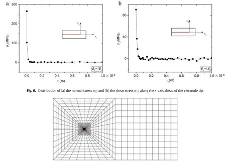
Fig.7.Finite element mesh of an electrically permeable crack emanating from the electrode.
Figure6showsthedistributionofthenormalandshearstresses ahead of the electrode tip along thex-axis in actuators subjected to electric field 1Ec.Concentrations of both normal and shear stresses are found whenx1approaches the electrode tip.The stress singularity can be attributed to two aspects.One is the discrepancy of deformations between active and inactive regions. When ferroelectrics are actuated,the active region covered by electrodes induces deformations by piezoelectric effect,while the inactive region is never exposed to the electric field.The incompatibility of deformation between two regions leads to the tension and bending of the inactive regions and in this way introduces the concentrations of tensile and shear stresses near the electrode tips.On the other hand,a large degree of domain switching is significantly induced around the electrode tip as shown in Fig.5(e).The incompatibility of strain near the electrode tip may cause domain switching,thereby changing the local electrical domain structure.The change of local domain structure changes the internal electric field and the internal stress near the electrode tip because spontaneous strains are accompanied with polarization domain switching.
As discussed above,the preferred domain switching near the electrode tips can lead to a prominent spontaneous strain and thus enhances the concentration of residual stress.A crack can emanate from an internal electrode and finally damaging the multilayer ferroelectric actuators[17].If a conducting piece migrates on the freshly created crack surface,the crack itself becomes a conducting sheet.In this work an electrically permeable crack is numerically simulated and domain structure induced by cracking is observed by means of the present micromechanical FEM.Due to the symmetry,a crack tip area between two ferroelectric layers is modeled and meshed with the refine mesh around the crack tip as shown in Fig.7.
Figure 8 shows the sizes and shapes of switching zones around the crack induced by mechanical actuating strain,where the direction of actuating strain is perpendicular to the crack surface.It is found that a polarization switching zone is formed if the actuating strain exceeds a critical value even though the electrical field is absent.The state of stress concentration first reaches domain switching criteria near the crack tip.The shape of switching zone appears two symmetrical wings forwards.It is interesting to find that the tendency of switching zone is approximately along 45°to the crack surface,where the maximum values of stress exist and induces the maximum dissipative switching energy.Obviously,the larger the actuating strain is,the larger the switching zone will be.The size of switching zone even reaches the scale of crack length with increasing actuating strain.
Figure 9 illustrates switching zones around the crack under the applied electric field,where the direction of electric field is perpendicular to the crack surface.Similar conclusions can be drawn as in Fig.8.The larger the electric field is,the larger the switching zone will be.Even a small electric load can lead to a large domain switching zone.These findings are different from the traditional analysis of the characteristic size of switching zone based on the small scale switching conditions[20],where a small domain switching zone was calculated based on the assumption that the deriving voltage is low enough so that the electromechanical behavior of the ceramic bulk is linear except for a small radius around the crack tip.The present results indicate that the previous analysis underestimate the role of crack on domain switching structure.A large scale domain switching zone exists in the vicinity of crack tip even though a small magnitude of electromechanical loading is applied.

Fig.8.Domain switching zone around the electrically permeable crack under different actuating strainsε22(a)0.004%,(b)0.006%,(c)0.008%.

Fig.9.Domain switching zone around the electrically permeable crack under different electric fields(a)0.3Ec,(b)0.5Ec,(c)0.7Ec.
A micromechanical nonlinear constitutive model is used to simulate domain switching around the electrode tip and an electrically permeable crack tip in multilayer ferroelectric actuators.OneGaussianpointisconsideredas agraincomprisinga setofdistinctdomainvariantsinfiniteelementcalculation.Energy dissipation is responsible for domain switching barriers such as the critical energy release density to switch a crystallite.The electric field has a significant influence on concentration of stress ahead of electrode tips due to the incompatible strain as well as spontaneousstrain.Thelargertheactuatingstrainandelectricfield are,the larger the switching zone will be.A large scale of domain switching zone is found around an electrically permeable crack emanatingfromaninternalelectrode.Itindicatesthattheprevious analysis of crack problem under the small-scale domain switching saturation condition will not give useful estimate,especially when thedomainzoneiscomparabletothecracklength.Therefore,large scale switching theory has to be introduced.The results of this work provide a basic understanding on domain switching near the electrode tips and the crack tips in multilayer ferroelectric actuators.
Acknowledgments
This work was supported by the National Natural Science Foundation of China(11472205)and the Fundamental Research Funds for the Central Universities in China.
[1]F.Claeyssen,R.L.Letty,Performance and applications of actuators based on multilayered piezoceramics and shell structures,in:N.Setter(Ed.), Piezoelectric Materials in Devices,EPFL,2002,pp.103–122.
[2]K.Lubitz,C.Schuh,T.Steinkopff,et al.,Material aspects for reliability and life time of PZT multilayer ceramics,in:N.Setter(Ed.),Piezoelectric Materials in Devices,EPFL,2002,pp.183–194.
[3]A.Furuta,K.Uchino,Dynamicobservationofcrackpropagationinpiezoelectric multilayer actuators,J.Am.Gram.Sot.76(1993)1615–1617.
[4]H.Aburatani,S.Harada,K.Uchino,et al.,Destruction mechanism of ceramic multilayer actuators,J.Appl.Phys.33(1994)3091–3094.
[5]J.Rödel,T.U.Darmstadt,unpublished work,2013.
[6]W.Yang,Z.Suo,Cracking in ceramic actuators caused by electrostriction,J. Mech.Phys.Solids 42(1994)649–663.
[7]Y.Shindo,M.Yoshida,F.Narita,et al.,Electroelastic field concentrations ahead of electrodes in multilayer piezoelectric actuators:experiment and finite element simulation,J.Mech.Phys.Solids 52(2004)1109–1124.
[8]K.M.Jeong,H.G.Beom,Cracking in ferroelectric ceramic actuators caused by domain switching,Int.J.Appl.Electromag.Mech.24(2006)115–127.
[9]X.J.Zhao,B.Liu,D.N.Fang,Study on electroelastic field concentration around the electrode tip in multilayer ferroelectric actuators of two designs and their optimizations,Int.J.Plast.26(2010)533–548.
[10]T.Y.Zhang,M.H.Zhao,P.Tong,Fracture of piezoelectric ceramics,Adv.Appl. Mech.38(2002)147–289.
[11]Y.H.Chen,T.J.Lu,Cracks and fracture in piezoelectrics,Adv.Appl.Mech.39 (2003)121–215.
[12]M.Kuna,Finite element analyses of cracks in piezoelectric structures-a survey,Arch.Appl.Mech.76(2006)725–745.
[13]M.Kuna,Fracture mechanics of piezoelectric materials—where are we right now?Engng.Fract.Mech.77(2010)309–326.
[14]M.Kamlah,A.C.Liskowsky,R.M.McMeeking,et al.,Finite element simulation of a polycrystalline ferroelectric based on a multidomain single crystal switching model,Int.J.Solids Struct.42(2005)2949–2964.
[15]A.Pathak,R.M.McMeeking,Three-dimensional finite element simulations of ferroelectric polycrystals under electrical and mechanical loading,J.Mech. Phys.Solids 56(2008)663–683.
[16]J.E.Huber,N.A.Fleck,C.M.Landis,et al.,A constitutive model for ferroelectric polycrystals,J.Mech.Phys.Solids 47(1999)1663–1697.
[17]S.C.Hwang,R.M.McMeeking,A finite element model of ferroelectric polycrystals,Int.J.Solids Struct.36(1999)1541–1556.
[18]F.X.Li,D.N.Fang,Simulations of domain switching in ferroelectrics by a threedimensional finite element model,Mech.Mater.36(2004)959–973.
[19]M.Enderlein,Finite element method for fracture analysis of cracks in piezoelectric structures for transient electromechanical loads(Ph.D.Thesis), TU Bergakademie Freiberg,2007(in German).
[20]T.H.Hao,X.Gong,Z.Suo,Fracture mechanics for the design of ceramic multilayer actuators,J.Mech.Phys.Solids 44(1996)23–48.
E-mail address:qunli@mail.xjtu.edu.cn.
http://dx.doi.org/10.1016/j.taml.2016.11.005
2095-0349/©2016 The Author(s).Published by Elsevier Ltd on behalf of The Chinese Society of Theoretical and Applied Mechanics.This is an open access article under the CC BY-NC-ND license(http://creativecommons.org/licenses/by-nc-nd/4.0/).
*This article belongs to the Fluid Mechanics
杂志排行
Theoretical & Applied Mechanics Letters的其它文章
- Synergy to discovery and innovation—Growth of nanorods
- Buckling and post-buckling analyses of size-dependent piezoelectric nanoplates
- Coriolis effect on responses of rotating thin piezoelectric hollow cylinder
- On the role of piezoelectricity in phonon properties and thermal conductivity of GaN nanofilms
- On transition of type V interaction in double-wedge flow with non-equilibrium effects
- Numerical simulation of Gurney flap on SFYT15thick airfoil
