A Wafer Level Chip on Board Package Based on Anodic Alumina Substrate*
2016-11-08LIUMifengWUWeiweiRENWeipengWANGLichunShanghaiAerospaceElectronicandCommunicationEquipmentResearchInstituteShanghai201109China
LIU Mifeng,WU Weiwei,REN Weipeng,WANG Lichun(Shanghai Aerospace Electronic and Communication Equipment Research Institute,Shanghai 201109,China)
A Wafer Level Chip on Board Package Based on Anodic Alumina Substrate*
LIU Mifeng*,WU Weiwei,REN Weipeng,WANG Lichun
(Shanghai Aerospace Electronic and Communication Equipment Research Institute,Shanghai 201109,China)
A novel chip on board(COB)technology based on thin anodic alumina substrate is proposed.The 0.1mm thickness anodic alumina substrate is developed by oxalic anodized method with 60 V voltage and 30℃temperature,and the line width,resistance of Al interconnect and insulation resistance between Al interconnects are 35 μm,below 1 Ω/cm and over 1×10¹⁰Ω,respectively.The wafer-level COB wafer,which includes an anodic alumina wafer and flash chips,is achieved by chip-on-chip SMT,and the yield is over 93%.Finally,a NAND Flash module has been developed.Furthermore,the COB package technology based on anodic alumina substrate has a wide application prospect.
3D package;COB;anodic alumina;packaging substrate
EEACC:0170J doi:10.3969/j.issn.1004-1699.2016.10.009
With development of miniature and multi-functional device,the electronic systems sets higher requirement of packaging density.Therefore,system-inpackage(SiP)technology is attracting more attention,because of the higher packaging density and flexibility.Chip on board(COB)is not only used for LED package and high heat dissipation package,but also can be applied to 3D package[1-7].The common COB,which used PCB,LTCC,glass and ceramics,is not suitable for 3D package,due to the thick substrate thickness,poor thermal conductivity and CTE mismatch.As the most common metal,aluminum has excellent thermal and electrical properties,and aluminum can greatly improve the surface abrasion resistance,corrosion resistance and insulating properties after anodizing treatment[8].Therefore,the anodized aluminum substrate is suitable for package[9-12].In this work,we present a COB packaging technology based on anodized aluminum substrate,which has the advantage of thinner thickness,CTE match and high thermal conductivity.
1 Anodic alumina substrate
1.1Aluminum anodized
Compared to single-sided anodized method,bothsided anodized method can shorten the time in half,and can balance the stress of the substrate to prevent warp-ing.An oxalic acid anodizing system is built for doublesided anodized aluminum,as shown in Fig.2,and a dualflume structure is used in the system.The inner flume is filled with 5 wt.%oxalic acid,which contains two cathode(Ti plates)and one anode(Aluminum wafer),and the outer flume is connected with circulation cooling device to maintain the temperature of oxalic acid.
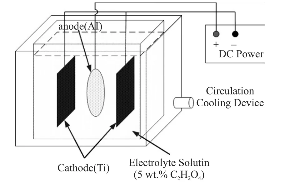
Fig.1 Both-side anodized aluminum system
The anodized aluminum rate increases as the voltage or the temperature of solution rises,but if the voltage or the temperature of solution is too high,the burnout failures will occur at the porous alumina,because of the heat transfer is not in time in the pores of porous aluminum[10-12].In order to decrease the fabrication time of anodic alumina,the 0.1mm thick,4 inch aluminum wafers are anodized under different temperature of solution(20℃,25℃ and 30℃),5 wt.%oxalic acid and 60 V applied voltage.Total time of complete anodized aluminum is approximately 20 h,12 h and 6 h,respectively.And all the samples have uniform colour surface and do not found burnout defect,as shown in Fig.2.Therefore,the anodic parameter of 30℃,5 wt.%oxalic acid and 60 V voltage is used in the fabrication of anodic alumina substrate.

Fig.2 Optical microscopic image of anodic alumina
1.2Fabrication and test
The fabrication process of anodic alumina substrate,as shown in Fig.3,includes aluminum wafer pretreatment,formation of barrier layer and both-side anodized aluminum.The process is as follow:
①A 0.1 mm thickness,4 inch Al wafer(GB.8011)is cleaned in deionized water and acetone solution 10 min with ultrasonic,respectively,in order to remove the pollution on the wafer surface,as shown in Fig.3(a).
②After the initial cleaning process,the barrier Al2O3layer is formed by lithography and anodic oxidation(5℃,1 wt.%citric acid solution and 120 V applied voltage),which acts as a temporary barrier layer during both-side anodized aluminum,as shown in Fig.3(b).
③The surface of pad area is covered by photoresist through lithography,as shown in Fig.3(c).
④The both-side anodized aluminum process is carried on,and the temporary barrier layer is dissolved after 1 hour,then the Al interconnect area begin anodizing,as shown in Fig.3(d);
⑤The both-side anodized aluminum process completes after 6 hour,and only interconnect region and pad region remain un-oxidized aluminum,while other regions are formed of porous alumina.Then,photoresist covered on pad is removed by acetone solution,and the preparation of anodic alumina substrate is finish,as shown in Fig.3(e).
The anodic alumina substrate is successfully prepared,and the minimum line width of Al interconnect is 35 μm,as shown in Fig.4.The property test of anodic alumina substrate is carried on by semiconductor Parameter Analyzer,and the resistance of Al interconnect is below 1 Ω/cm and insulation resistance between Al interconnects is over 1×10¹⁰Ω.
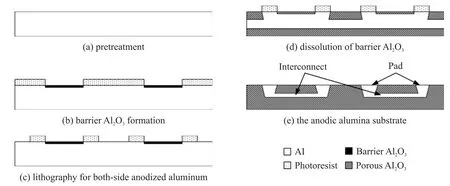
Fig.3 Schematic of the fabrication process
2 Wafer level COB Package
2.1Anodic alumina wafer for flash chip
In this paper,Samsung 4 Gb NAND flash chips(300 μm thickness)are used in COB packaging experiments.According to the features of single side pad arrangement of flash chip,the chip on chip packaging solution is available and increases packaging density.Meanwhile,the test pad is considered during the substrate layout,to achieve the ability of COB module wafer-level test.Then,the anodic alumina wafer,as shown in Fig.5,is fabricated by the process above mentioned.
2.2Assembly
Each die of the anodic alumina wafer mounts two flash chips by Allteck WEST·BOND 7200CR-79,and the top chip moves parallel 0.5 mm distance,in order to expose the pad of bottom chip,as shown in Fig.6(a).Then,the bilayer Au wire bonding process is carried on by Allteck WEST·BOND 7476E-79,as shown in Fig.6(b).The bonding joints of Al pad show good mechanical characteristics with pull stress of 6.1 to 9.4 g by Allteck WEST·BOND 70PTE.
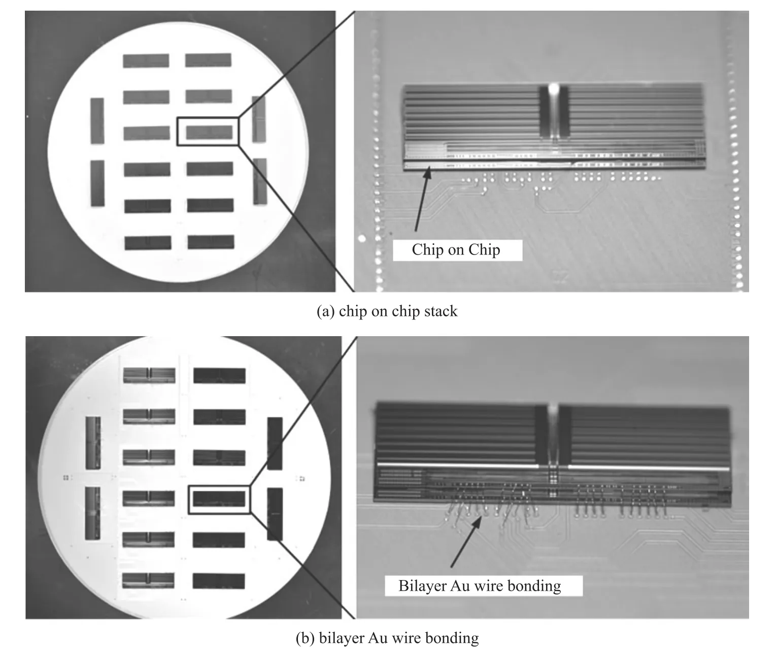
Fig.6 COB wafer microassembly
3 Result and Discussion
The electrical performance test system for COB wafer is based on Cascade Microtech 9 000 Analytical Probe Station,as shown in Fig.7(a).The realization of electrical interconnection between COB test pad and test development board depends on two 25 pin probe card and 50 wire ranging.According flash chip manual,the test program flow include erase test,write test and read test,and the qualified COB die should satisfy that read data is same with write data,as shown in Fig.7(b).A COB package wafer is fabricated,which involve contains 16 COB die,and the yield is over 93%.
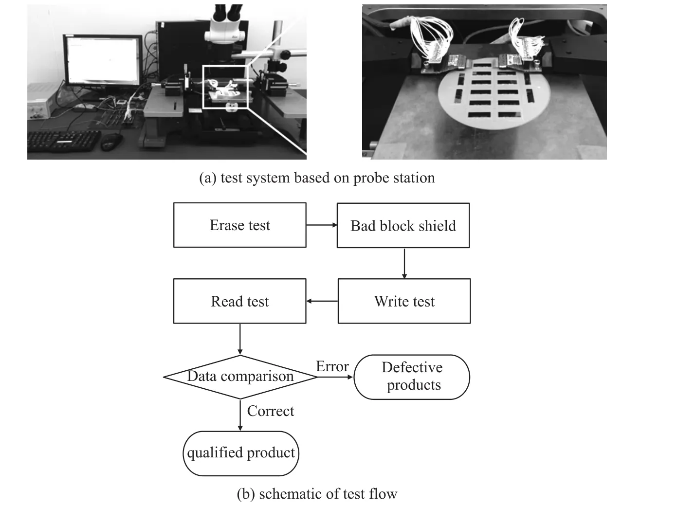
Fig.7 The electrical performance test of COB wafer
For verify the application prospect of COB package based on anodic alumina substrate,a 3D package flash module is proposed,which contains four COB modules by 3D stacking,as shown in Fig.8(a).The 32 G flash module is fabricated by 3D stacking epoxy potting and side metallization,as shown in Fig.8(b).The flash module is only 5.9 mm thickness(exclude pin)and has passed the performance test.
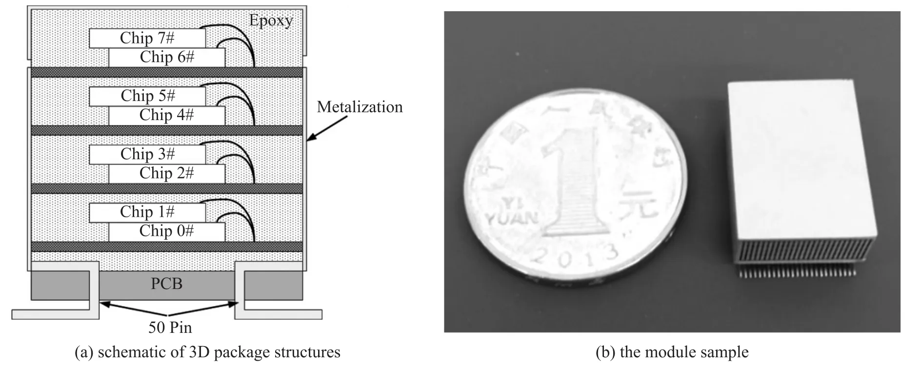
Fig.8 NAND Flash module 3D package,(a)schematic of 3D package structures,(b)the module sample.
4 Summary
The anodic alumina substrate is fabricated in 5 wt.%oxalic acid solution with the process parameters of 60 V voltage and 20℃~30℃temperature.The 35 μm line width,the 1 Ω/cm resistance of Al interconnect and 1×10¹⁰Ω insulation resistance between Al interconnects have been achieved.The 0.1 mm thickness,4 inch anodic alumina wafer is developed for Samsung 4 Gb NAND flash chip COB package.And the COB package wafer,which yield is over 93%,is assembled by using chip on chip process and bilayer Au wire bonding process.Finally,a 32 G flash module is proposed and realized by stacking of four COB package modules.Therefore,the COB package technology based on anodic alumina substrate has bright applied future in the field of system in package,due to the thinner thickness,matching CET,high density and low cost.
5 Acknowledgement
This work was supported by the National S&T Major Project of China under Grant 2014ZX02501016.
[1]Ganasan J R.3D Packaging-Combining Chip on Chip(COC)and Chip on Board(COB)Packages-Process and Design Considerations[C]//Electronic Components and Technology Conference,1997.Proceedings,47th IEEE,1997:1210-1213.
[2]Jinka K K,Ganesan S,Dasgupta A,et al.Chip-on-Board(CoB) Technology for Low Temperature Environments.Part I:Wire Profile Modeling in Unencapsulated Chips[J].Microelectronics Reliability,2007,47(8):1246-1250.
[3]Park J C,Yoo C S,Kang W,et al.GaN HEMT Based High Efficiency Push-pull Inverse Class-F Power Amplifier Using Chip-onboard Technique[C]//Microwave Conference Proceedings(APMC),2011 Asia-Pacific IEEE,2011:522-525.
[4]SimJK,AshokK,RaYH,etal.CharacteristicEnhancementofWhite LED Lamp Using Low Temperature Co-Fired Ceramic-Chip on BoardPackage[J].CurrentAppliedPhysics,2012,12(2):494-498.
[5]Juntunen E,Tapaninen O,Sitomaniemi A,et al.Copper-Core MCPCB with Thermal Vias for High-Power COB LED Modules[J].IEEE Transactions on Power Electronics,2014,29(3):1410-1417.
[6]李明,黄庆安,宋竞,等.COB封装中热-机械耦合效应的研究[J].传感技术学报,2006,19(5):1606-1609.
[7]Zhong Q,Fang L,Jian H E,et al.Study on the Junction Temperature and Thermal Resistance of LEDs Packaged on Anodized Aluminum Substrate[J].Semiconductor Optoelectronics,2010,31(6):842-845.
[8]徐国荣,唐安平.多孔阳极氧化铝的化学修饰及其应用于过氧化氢的测定[J].传感技术学报,2011,24(6):783-787.
[9]Kim K,Kim K,Hong S.MMICs and Front End Module Design with Selectively Anodized Aluminum Substrate[C]//Microwave Conference Proceedings(APMC),2013 Asia-Pacific IEEE,2013:438-440.
[10]Sulka G D,Stroobants S,Moshchalkov V V,et al.Effect of Tensile Stress on Growth of Self-organized Nanostructures on Anodized Aluminum[J].Journal of the Electrochemical Society,2004,151(5):B260-B264.
[11]Tong L,Cheng B,Liu Z,et al.Fabrication,Structural Characterization and Sensing Properties of Polydiacetylene Nanofibers Templated from Anodized Aluminum Oxide[J].Sensors&Actuators B Chemical,2011,155(2):584-591.
[12]Hyun-Chae N A,Sung T J,Yoon S H,et al.Formation of Unidirectional Nanoporous Structures in Thickly Anodized Aluminum Oxide Layer[J].Transactions of Nonferrous Metals Society of China,2009,4(4):1013-1017.

刘米丰(1984-),男,2012年毕业于中国科学院上海微系统与信息技术研究所,获博士学位。2012年起在上海航天电子通讯设备研究所工作至今,高级工程师,主要研究方向为系统级封装技术、先进MEMS封装工艺,mifengliush@sina.com。
基于阳极氧化铝基板的圆片级板载芯片封装技术*
刘米丰*,吴伟伟,任卫朋,王立春
(上海航天电子通讯设备研究所,上海201109)
提出了一种新型基于阳极氧化铝基板的板载芯片(Chip on Board)封装技术。在5 wt.%,30℃的草酸电解液中采用60 V直流电压,制备了0.1 mm厚度的阳极氧化铝基板圆片,铝导线最小线宽、电阻及导线间绝缘电阻分别为35 μm、小于1 Ω/cm与大于1×1010Ω。在超薄阳极氧化铝基板圆片进行了双层Flash裸芯片堆叠及金丝引线键合,实现了圆片级COB封装,成品率高于93%。最后,将COB单元进行三维堆叠封装,制备了32 Gb Flash模组。因此基于阳极氧化铝基板的板载芯片封装技术具有较大的应用前景。
三维封装;板载芯片;阳极氧化铝;封装基板
TN405;TN409
A
1004-1699(2016)10-1516-06
2016-4-21修改日期:2016-05-09
项目来源:国家科技重大专项项目(2014ZX02501016)
