基于低温共烧陶瓷的微机械差分电容式加速度计的研究*
2016-10-13张义川方孺牛唐小平卢会湘严英占金玉丰
张义川,缪 旻,*,方孺牛,唐小平,卢会湘,严英占,金玉丰
(1.北京信息科技大学信息微系统研究所,北京100101;2.北京大学微米/纳米加工技术国家级重点实验室,北京100871;3.中国电子科技集团公司第五十四研究所,石家庄050081)
基于低温共烧陶瓷的微机械差分电容式加速度计的研究*
张义川1,缪旻1,2*,方孺牛2,唐小平3,卢会湘3,严英占3,金玉丰2
(1.北京信息科技大学信息微系统研究所,北京100101;2.北京大学微米/纳米加工技术国家级重点实验室,北京100871;3.中国电子科技集团公司第五十四研究所,石家庄050081)
低温共烧陶瓷(LTCC)技术是实现电子设备小型化、高密度集成化的主流封装/组装集成技术,可适用于耐高温、耐受恶劣环境下的特性要求。报道了以LTCC为结构材料设计、制作的一种MEMS差分电容式加速度计。该器件的敏感质量、4根悬臂梁结构都内嵌于LTCC多层基板,质量块和上下盖板之间通过印刷电极组成差分电容对;高精度电容检测芯片表贴于LTCC基板表面,将差分电容信号转化为电压信号。论文讨论了微机械LTCC加速度计的设计与制备、检测电路和性能测试。LTCC的高密度多层布线减小了互连线的长度和相关耦合寄生电容;基于集成芯片的检测电路解决了分立式检测电路的引起噪声大、电路复杂等问题。测试结果表明:该加速度计结构灵敏度较高,小载荷情况下表现出良好的线性关系,灵敏度约为30.3 mV/gn。
低温共烧陶瓷;加速度计;微机械加工;三维集成;微系统
EEACC:7230M;2575Fdoi:10.3969/j.issn.1004-1699.2016.04.001
LTCC technology is used for fabricating sensors and actuators,especially for harsh environment due to its good physical-chemical properties,low costs,high reliability,and the possibility to create integrated threedimensional micro structures[1].Though applied as a good MEMS packaging material for over 20 years,it is only in recent years that LTCC became the structural material for these dynamic and vibrant applications. Both domestic and foreign researchers in previous studies in the past decade have found that micro-machining of LTCC can be achieved to the extent that the processed micromechanical functional structure may be three-dimensionally integrated to high density[2-3].
Micro(MEMS)accelerometer can be widely used to measure acceleration,inertial forces,and shock and has a large variety of applications,such as military,automobile industry,active stabilization.For harsh environment applications,silicon is not an ideal choice due to material property degradation at high temperature,but the exceptional material properties of LTCC materials make them an ideal choice for them.A piezoelectric LTCC uniaxial accelerometer was reported in the literature[4]and[5],the device consists of a thin LTCC round membrane with a fixed LTCC cylindrical seismic mass in the middle of the membrane,but its temperature drift is bigger and the stability is poor. This work focuses on a differential capacitive accelerometer using LTCC technology.Compared to the other types of accelerometer,differential capacitive accelerometer has the advantages of simple structure,good stability,low drift and high sensitivity.
1 The Design of the Accelerometer
The design of micro-accelerometer is usually based on the classic mechanical theory[6].There are already micro-accelerometer based on various operation principles,such as piezoelectric,tunnel,piezo resistive,and capacitive effects.The sensing element of the LTCC micro-accelerometer as proposed consists of three parts:a top cover,a bottom cover and middle beam-mass structure,as shown in Fig.1(a)and 1(b),which together come in the form of an ordinary LTCC laminate acting conventionally as a packaging or assembly substrate.The square shaped proof mass is suspended in the center by four beams connected to the fixed frame.The beams are designed into L shape folded beams which aims to reduce the volumes of structure compared with straight beam of the same length.The surfaces of middle mass and two plate covers are metallized and compose a pair of differential capacitors. The capacitive signals from the sensing element are extracted through the LTCC multilayer interconnection wires and conveyed to the signal detection/interfacing ICs mounting on the front of the LTCC laminates.
The accelerometer sensing element is made of 23 layers of LTCC green ceramic tape,among them,the 1st layer to the 4th layer are the upper plate cover,5th to the 19th layer are the beam-mass structure,the 20th layer to the 23th layer are bottom plate cover.In order to improve the sensitivity of the accelerometer,the cantilever beams are designed to be as thick as 3 layers of LTCC tape in the 17th to 19th floor,which is thinner than the 15-layer fixed frame,as thinner leaf springs can lead to a bigger deformation at the same overload input.The commercial LTCC green tape of DP951 is employed.The structure size is 10-100 times bigger compared with the similar structure of silicon,but accelerometer device and the signal detecting circuit can be integrated in a LTCC module by amounting them onto the LTCC laminates and taking the advantages of high density interconnecting capabilities of LTCC packaging technology,and canbeappliedtothecorrespondingfields.

Fig.1 Design of the sensing element
The accelerometer is a second order spring-mass damping system and the basic principle of it follows Newton's second law.In the rest position,capacitance formed between the proof mass and the bottom electrode as well as the proof mass and the top electrode are equal to each other.By the theory of electrostatic we can see that:

Where C1,C2represent the upper and bottom counter electrode's capacity,andd0represents the distance of movement of the two electrodes.εrepresents the relative dielectric constant;ε0represents the dielectric constant of vacuum,and A represents the area of the electrodes.When the z-axis acceleration input signal is exposed to the acceleration,the displacement ofd0will be in the z-direction.Both capacitances change,one increases,while the other decreases,then the differential capacitance can be calculated as follow:

ForΔd≤d0,using Taylor series expansion,neglecting higher order term,thus:

In the case of electrostatic actuation,considering parallel plate capacitor,the electronic force due to the applied voltageV0(t):

The electrostatic force of proof mass is:

When inertial load is applied,thus:

ForΔd≤d,thus:

Minus sign indicates that electrostatic force is a positive feedback and its direction is the same as the inertial force.So for this accelerometer of open-loop type,if the applied voltage increases gradually and when the electrostatic force is greater than the elastic force of beams,the pull-in will occur and this occasion requires particular attention.
2 Simulation
The mechanical behavior of the beam-mass structure is simulated by the ANSYS FEA software.A load of 1G acceleration is attempted on the sensor structure. The maximum displacement in Z-axis is2.956μmas showed in Fig.2(a),so

We can know that the sensitivity of accelerometer is about2.956 μm/g.Fig.2(b)shows the static strain distribution of the accelerometer under 1G inertial load.The maximum of the LTCC is about 1.923 mPa which is much lower compared to the flexural strength of LTCC.We can see that the strains are relatively concentrated on the corners of the L shaped beams.

Fig.2 Z-axis displacement and static strain analysis under inertial load(1G)
The modal analysis obtains the principal modal parameters representing structure dynamic behavior as well as the important basis for evaluating accelerometer performance.The designed structure has five resonant modes as shown in Table 1,the dynamic analysis of the beam-structure shows that the first natural frequency of the structure corresponds to a resonance in the z-direction with a frequency of 292 Hz.In the second and third modes,the mass shows twist on X-and Y-axis along the center of the mass plane respectively and their resonant frequency is about 639 Hz.The fourth and fifth modal frequencies are far from the primary.The harmonic response analysis is shown in Fig 3. The resonant modes do not appear under Z-direction load(1G)except for the first model frequency.So we can conclude that the structure performs an excellent dynamic stability and anti-interference ability.

Table 1 Modal Analysis For The Ltcc Accelerometer
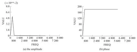
Fig.3 Harmonic response analysis of the accelerometer
3 Fabrication Process
The whole LTCC accelerometer module is completely fabricated in LTCC process and steps are as follows:
①Vias.Vias are punched by a laser in the green sheets for connections between layers.The square mass and beam structure are patterned by micromachining. The via diameter is200 μmas shown in Fig.4(a).
②Via filling.Via filling is the process in which the via holes formed in the green sheet are filled with the conductor.
③Screen-printing of conductive layers.A wiring conductor pattern is formed in alignment with the screen printing technique using Ag/Pd paste,the printed trace is250 μm.
④Laminating.Many layers of these printed green sheets are arranged in layers,and heat and pressure is applied to laminate them.
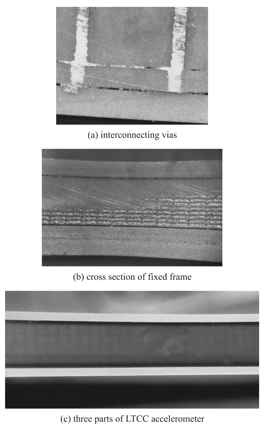
Fig.4(a)interconnecting vias;(b)cross section of fixed frame;(c)three parts of LTCC accelerometer
⑤Cofiring.The three parts of LTCC accelerometer (upper cover,bottom cover,middle beam structure)sintering respectively.Finally,with the glass as the bonding material,three parts bonding after sintering as shown in Fig.4(b)and Fig.4(c).Alignment accuracy isthe key and the most important step in this process,because the three parts are required to guarantee the effective interconnection of the signal.
⑥Devices mounting.The signal detecting/interfacing chip(MS3110)and other devices are mounted on the LTCC substrate by reflow process.
The alignment of laminated sheets,temperature of isostatic press and size of pressure have vital influence on the quality of product[7],so it is necessary to pay attention to the laminating process.The firing shrinkage and the variation thus induced in the substrate as a whole is one of the most important technical challenge in the cofiring process[8],and the deformation of beam and chamber collapse is another one.To solve this problem,this paper add auxiliary beams as supporting medium to solve this challenge and use laser to cut the extra beams after cofiring.X ray photograph of the accelerometer is showed in the Fig.5,sample of the accelerometer is showed in the Fig.6.

Fig.5 X-ray photograph of the accelerometer
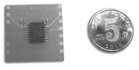
Fig.6 sample of the accelerometer
4 Capacitance Read-out Circuitry
Due to the small size of micro-accelerometer,the change of sensor capacitance becomes more smaller,complicating the design of readout circuit.However,parasitic capacitance is the main factor which restricts the precision of accelerometer system,so it needs to analyze the main sources in the system[9].Primary sources of parasitic capacitance include capacitance between bonding pads and substrates,and capacitance between interconnection lines and substrates[10-11].The methods of suppressing the parasitic capacitance usual are isolation,feedback,virtual ground and other methods.In order to facilitate the use of the improved circuitry,this paper adopted the integrated chip MS3110 as the capacitance detection/interfacing circuit,through the reasonable component layout,the necessary isolation technology ensured the good stability and anti-interference capacity of the whole system.TheMS3110 has high resolution,high stability,low drift,and more importantly it is adjustable internal balancing capacitor.The sensor is positioned very close to MS3110 chip to minimize the distance of transmission line.The theory of operation of the MS3110 IC can be summarized by the block diagram below in Fig.7.The chip is composed of capacitor compensation circuit,electric charge integral circuit,low pass filter and operational amplifier.the chip internal carrier generator generates two identical frequency,the same amplitude and the reverse phase high frequency carrier signal loaded on the measured capacitance(CS2IN,CS1IN)and the reference capacitor(CS2,CS1),and then the induction voltage signal in CSCOM through the current integrator,low-pass filter,amplifier circuit to get output voltage signal.
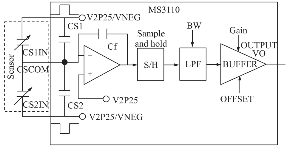
Fig.7 The block diagram of the MS3110
The output voltage can be described by a function of the sensing capacitances CS1T and CS2T,as shown by the following expression:

Where:CS1T=CS1IN+CS1,CS2T=CS2IN+CS2,thus

Then apply(4)and(11)on(10),thus

CS1IN and CS2IN are the input from the sensing element.CS1 and CS2 are internal adjustable capacitances that are used to balance the capacitance difference of the external capacitances to ensure the circuit is operating in the normal range[12].CF is selected to optimize the input sense capacitance range(CF≥1.5 pF),MS3110 has a low pass filter that can be programmable between 500 HZ~8 000 HZ.V0is the output Voltage,VREF can be set to 0.5 V or 2.25 V DC.Gain is 2 or 4. The calculated voltage is directly proportional to the displacement d in eq.(12).
Fig.8 demonstrates the experimental setup for capacitive sensing using the AT89S51.The P1.1 port is connected with the SCLK of MS3110 chip to provide the required clock,and the P1.0 port is connected to the SDATA of the MS3110 chip which is required to write in the 60 bits of data.In order to ensure the chip can work normally,the V2P25 reference voltage should be trimmed to 2.25 V+-10 mV and this reference voltage is provided by the voltage regulator chip LM1117-ADJ.
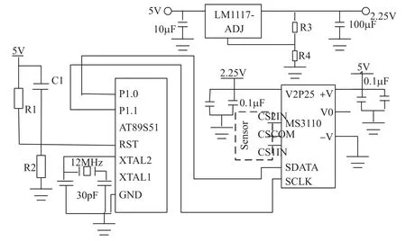
Fig.8 The diagram of signal processing circuit
The software designs adopt C51 language to compile data.There are two programming modes of MS3110IC:volatile registers write mode and an EEPROM programming mode.The first mode does not require extra power supply except the 5 V that is needed to power the chip,while once the power is off or the chip is reset,all the programming data will be lost.The second mode requires a 16 V power supply to write the data into EEPROM memory map and can program the internal EEPROM to store the values.Considering the actual apply,this paper adopts the first mode,and the software process as shown in Fig.9.

Fig.9 Software process
5 Measurement Results
A test platform is built to verify the static characteristics of the accelerometer as shown in Fig.10(a).In the room temperature environment,the integrated accelerometer-circuit system is fixed on the precision grating optical indexing head,and the input of different acceleration is realized by changing the angle between the sensitive axis and the direction of gravity.Six Points Method was adopted to achieve the measuring and calculation of volt.Dual tracking stabilized powersupply(DH1718D-2)provide the+5 V DC voltage,whiledigitaloscilloscope(TektronixTDS3012B)sampling the output analog voltage.Finally,the testing demonstrates that such a multi-ranged sensor has a good linearity and the voltage sensitivity is about 30.3 mV/gnas shown in Fig.10(b).

Fig.10 Picture of the test platform and acceleration in Z axis(gn)
6 Conclusion
A differential capacitive accelerometer embedded in LTCC packaging substrate is presented in this paper. The design,simulation and fabrication are introduced. The results of finite element analysis shows that the accelerometer may performs well in both static and dynamic mechanical characteristics.Test of prototype samples showed a good linearity and the voltage sensitivity is about 30.3 mV/gn.Right now,the improvement of the design and harsh environment performance test is under way.Micro-accelerometers made of Low Temperature Cofired Ceramics(LTCC)promise a higher temperature range and lower costs in small-volume production.
Acknowledgement
The present work is funded by the National Natural Science Foundation of China(61176102),the Importation and Development of High-Caliber Talents Project of Beijing Municipal Institutions(Great Wall Scholar,CIT&TCD20150320),and National Natural Science Foundation ofChina(61404119).
[1] Yang B C,Hu Y D.Overview on LTCC Technology and Its Development[J].Electronic Components and Materials,2014,11:5-10.
[2] Le K,Tan Y,Lama Y C.Overview on Fabrication of Three-Dimensional Structure sin Multi-Layer Ceramic Substrate,[J].Journal of the European Ceramic Society,2010,30:1973-1987.
[3] Miao M,Jin Y F,Gan H.Investigation of a Unified LTCC-Based Micromachining and Packaging Platform for High Density/Multifunctional Microsystem Integration[C]//The 62nd Electronic Components and Technology Conference(ECTC 2012),377-384.
[4] Jurkow D,Abrowski A D.Preliminary Model and Technology of Piezoelectric Low Temperature Co-Fired Ceramic(LTCC)Uniaxial Accelerometer[J].International Journal of Applied Ceramic Technology,2013,10:395-404.
[5] Jurkow D.Three-axial Low Temperature co-Fired Ceramic Accelerometer[J].Microelectronics,2013,30:125-133.
[6] Zheng X D,Cao X C.Study of a Novel Micro-Machined Capacitive Accelerometer[J].Chinese Journal of Sensors and Actuators,2008(2):226-229.
[7] Zhao F,Dang Y L.Analysis of Key Technology in LTCC Circuit Fabrication[J].Electroionic Process Technology,2013(1):37-39.
[8] Dominik J,Thomas M.Overview on Low Temperature co-Fired Ceramic Sensors[J].Sensors and Actuators A,2015:125-146.
[9] Yin T,Yang H G.Study on MEMS Precision Capacitive Readout Circuits Design[J].Chinese Journal of Electron Devices,2007 (4):1199-1193.
[10]Xu P,Zhang Y.Research on Detection of Differential Capacitance Based on Ms3110 and EMC Design[J].Instrument Technique and Sensor,2008(5):60-62
[11]Wang Y H,Li X Y.Synthetic Analysis of Noise in Capacitive Micro-Accelerometer[J].Chinese Journal of Sensors and Actuators,2008(4):648-651.
[12]Wang J J,Luo P.High-Precision Differential Capacitance Detecting Circuit for MEMS Acceleration Sensors[J].Journal of Wuhan University of Technology,2004,26:10-16.

张义川(1991-),男,汉族,硕士研究生,2013年于山东师范大学获学士学位,现就读于北京信息科技大学,主要从事低温共烧陶瓷MEMS微加速度计的研究,772514953@qq.com;

缪旻(1973-),男,汉族,博士,教授,2005于北京大学获博士学位。主要从事信息与通信工程、微米/纳米加工、微电子学与固体电子学、高等教育学等方面的研究,miaomin@bistu.edu.cn。
A Capacitive Micro-Accelerometer Based on LTCC Laminates*
ZHANG Yichuan1,MIAO Min1,2*,FANG Runiu2,TANG Xiaoping3,LU Huixiang3,YAN Yingzhan3,JIN Yufeng2
(1.Information Microsystem Institute,Beijing Information Science and Technology University,Beijing 100101,China;2.National Key Laboratory of Science and Technology on Micro/Nano Fabrication,Peking University,Beijing 100871,China;3.The 54th Institute of China Electronic Technology Group Corporation,Shijiazhuang 050081,China)
With the development of the miniaturization and high density integration of electronic devices,Low Temperature Co-fired Ceramic(LTCC)technology is becoming the mainstream technology for microelectronic and micro/ nano multifunctional device packaging and assembly.This paper presents a capacitive micro-accelerometer embedded into LTCC packaging substrate.Its square shaped proof mass of the sensing element is suspended in the center by four folded beams which are connected to the frame.The design,simulation,fabrication,and performance test of the accelerometer are discussed.High density multilayer wiring supported by LTCC microfabrication reduces the length of the interconnect line between sensing elements and circuitry and the associated parasitic capacitance.The signal detecting circuit based on the integrated chip solves the problem of large noise,circuit complexity,and so on. The test results show that the accelerometer has sufficient sensitivity and good linear relationship at low overload and the sensitivity is about 30.3 mV/gn.
accelerometer;ceramic micromachining;three-dimensional integration;microsystem
TH824;TP212.1
A
1004-1699(2016)04-0467-07
项目来源:国家自然科学基金项目(61176102,60976083,60501007,61404119);北京市属高等学校高层次人才引进与培养计划项目(CIT&TCD20150320);北京市自然科学基金项目(3102014)
2015-11-19修改日期:2015-12-20
