脉冲激光沉积制备SrSn1-xCoxO3外延薄膜的微结构表征及能带调控
2016-09-05虎学梅高相东李效民顾正莹吴永庆上海大学材料科学与工程学院上海00444中国科学院上海硅酸盐研究所高性能陶瓷与超微结构国家重点实验室上海00050
虎学梅 高相东 李效民 顾正莹 施 鹰 吴永庆(上海大学材料科学与工程学院,上海00444;中国科学院上海硅酸盐研究所,高性能陶瓷与超微结构国家重点实验室,上海00050)
脉冲激光沉积制备SrSn1-xCoxO3外延薄膜的微结构表征及能带调控
虎学梅1,2高相东2,*李效民2顾正莹2施鹰1吴永庆2
(1上海大学材料科学与工程学院,上海200444;2中国科学院上海硅酸盐研究所,高性能陶瓷与超微结构国家重点实验室,上海200050)
钙钛矿结构SrSnO3因其独特的介电和半导体性质而备受关注,通过掺杂可显著调控其电学、磁学性能,拓宽其应用范围。本研究在单晶SrTiO3(001)衬底上通过脉冲激光方法外延生长了SrSn1-xCoxO3(x=0, 0.16,0.33,0.5)(SSCO)薄膜,探究了Co含量对薄膜结晶性、微观结构、光学性能以及介电性能的影响。结果表明,SrSn1-xCoxO3薄膜可在SrTiO3(001)衬底上外延生长,Co掺杂不会导致薄膜结晶质量的劣化。薄膜表面形貌平整、致密,膜厚200 nm,表面粗糙度为0.44 nm。随薄膜中Co掺杂量增加,薄膜透过率从90%降至25%,光学带隙从4.24 eV降至2.44 eV。介电性能测试表明,掺杂薄膜在106Hz时介电常数为70.1,比无掺杂SrSnO3薄膜提高57%。室温时SSCO薄膜表面电阻率为172 MΩ,在1000°C范围内薄膜结构稳定。
碱土锡酸盐;物理气相沉积;薄膜;外延生长;光学带隙
[Communication]
www.whxb.pku.edu.cn
1 Introduction
Alkaline earth stannates MSnO3(M=Sr,Ba,Ca)are a class of materials possessing the perovskite structure and outstanding dielectric and sensing properties,whichcanbe usedinmanyfields including capacitors,moisture sensors,and solar cells1-4.In contrast with the pure MSnO3,the doping of MSnO3has attracted more interests of researchers,as the perovskite structure of MSnO3provides an ideal hosting matrix for the doping of metal elements to form functional materials5-10.Various metal elements including La,Sb,and Er were doped at M or Sn site of MSnO3to tune its optical,electrical,and magnetic properties11-13.Among the three types of MSnO3,SrSnO3has received more attention due to its higher band gap(4.27 eV)than BaSnO3(3.00 eV)and CaSnO3(3.87 eV)14-17.Many studies focused on the doping of SrSnO3to prepare transparent conductive oxide films18,19.For example,Liu et al.20grew epitaxial Sb-doped SrSnO3films on SrTiO3(STO) (001)substrates via pulsed laser deposition(PLD),and stressed its potential in high optical transmittance and good conductivity. Nd-doped SrSnO3films were also epitaxially grown on SrTiO3(001)substrate with Nd substituting for A-site Sr21,which also exhibited good transparency and conductivities.However,while there are active studies in tuning the optical and electrical properties of SrSnO3film,few researchers focused to modulate its band gap.Based on the calculations on the electronic structure,Shein et al.22reported that SrSnO3doped with Fe and Co may have a smallerbandgap,withthebandgapaslowas0.7eVforSr2SnFeO6. The epitaxial growth of SrSn1-xFexO3films were realized on MgO substrate and the decreasing trend of the optical band gap with increasing Fe content were observed23.However,no further work has been reported on Co doped SrSnO3thin films with controllable band gap.
In this paper,we prepared SrSn1-xCoxO3(x=0,0.16,0.33,0.5) (SSCO)films on single crystal SrTiO3(001)substrate by the pulsed laser deposition method,and investigated the crystallinity,microstructure,optical and dielectric properties of the films in detail. Our aim is to explore a feasible route to grow high crystalline SSCO films,to acquire the basic information on its microstructure and physical properties,and to promote their further applications in photoelectrical devices.
2 Experimental
SSCO thin films were grown on STO(001)single crystal substrate using the pulsed laser deposition(PLD)technique.SSCO ceramic disks(x=0,0.16,0.33,0.5)were used as the targets, which were sintered at 1250°C for 24 h in a solid-state reaction route by using SrCO3(99.9%,Aladdin),SnO2(99.8%,Aladdin) and Co2O3(99.8%,Aladdin)powders as the starting materials.The substrates ultrasonicly rinsed in water,alcohol and acetone successively before deposition.The laser source was a 248 nm KrF excimer laser(Lamda physik Compex 201,Germany)with the repetition rate of 5 Hz and energy density of 200 mJ∙pulse-1.The deposition lasted for 1.5 h.The substrate temperature was fixed at 650°C and the oxygen pressure was set at 0.1 Pa.For the measurement of optical properties,SSCO films with the same deposition parameters were grown on the quartz substrate.
X-ray diffraction(XRD)technique(Bruker D8,Cu Kα1radiation,Japan)was used to characterize the crystallinity.The film morphologies were investigated by scanning electron microscopy (SEM,Hitachi S-4800,Japan)and atomic force microscopy (AFM,SΙΙ SPI-3800I,Japan).Optical transmittance were measured with a spectrophotometer(Hitachi,U-4100,Japan)using a bare quartz glass slide as the reference.The dielectric properties were measured using an Aglient 4294A Tester LCR meter (America)at room temperature.

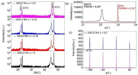
Fig.1 (a)XRD patterns of SrSn1-xCoxO3films deposited on STO(001)substrate;(b)ω-scan rocking curve on(002)peaks of SrSn0.5Co0.5O3and STO(001)substrate;(c)φ-scan patterns of SrSn0.5Co0.5O3and STO(001)substrate around(202)reflections
3 Results and discussion
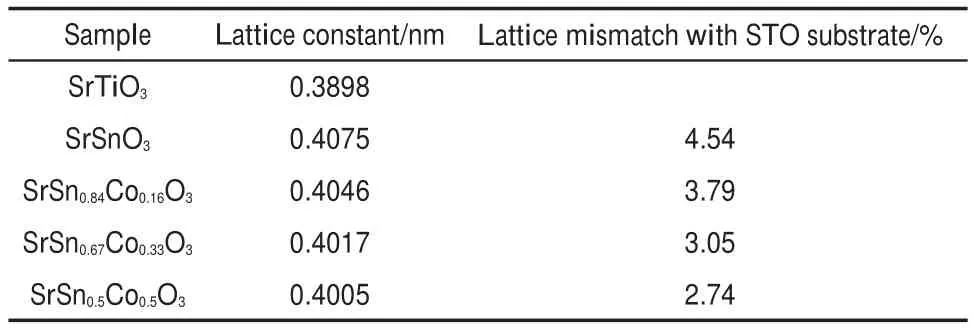
Fig.1(a)illustrates XRD patterns of SSCO films grown on STO (001)substrate with different Co doping level(x=0,0.16,0.33,0.5).Only the reflection peaks from the(00l)plane of SSCO films and STO(001)substrates were detected,suggesting the high crystalline quality of the films and the highly preferential orientation along c-axis.With the x value changing from 0 to 0.5,the value of the diffraction peak along(00l)plane increased gradually, indicating that Co atoms substituted for Sn atoms which affected the lattice parameters of SrSnO3.Fig.1(b)shows the ω-scan rocking curve of the film with x value of 0.5,and the full width at half maximum(FWHM)of(002)peak was 0.04°,further testifying the high crystallinity of the film.The φ-scan patterns of SSCO film(x=0.5)and STO(001)substrate to study in-plane ordering,and a set of four distinct peaks at an interval of 90°was observed in Fig.1(c),indicating that the SSCO film was grown epitaxially on the STO(001)substrates in a cube on cube relationship.According to the SSCO(00l)reflections,the SSCO thin film lattice constants with different x values were calculated and lattice mismatch with STO(001)substrate were shown in Table 1.
All the SSCO films exhibited similar morphology.Fig.2(a) illustrates typical SEM image of the SSCO film(x=0.5)on the cross section.A very dense microstructure was observed clearly, and the film thickness was 200 nm.AFM image over the area of 5 μm×5 μm was shown in Fig.2(b),which presented a rather smooth morphology,with root-mean-square roughness(rms)of 0.44 nm and an average particle size of 3.4 nm.

Table 1 SrSn1-xCoxO3film lattice constant and lattice mismatch

Fig.2 (a)SEM image on the cross section and(b)AFM image on the surface of SrSn0.5Co0.5O3deposited on STO(001)substrate

Fig.3 (a)Transmittance spectraof SrSn1-xCoxO3films depositedonquartz(theinsetshowing thephotographs of SrSn1-xCoxO3filmsamples); (b)(hvα)2-hv plotsof thefilmsderived from(a)
Because STO(001)substrates have the band gap of 3.2 eV lower than that of SrSnO3film,which makes it impossible to evaluate the band gap of SSCO films higher than the substrate.So we grew SSCO films on quartz substrates with the same conditions,to obtain the transmittance properties of the films roundly and precisely.It was found that the optical absorption trend of the SSCO films on quartz substrate was similar to that on STO substrate,though the epitaxial growth of SSCO films was not replicated on quartz substrate.Fig.3(a)shows the transmittance spectra of SSCO films grown on quartz in the range of 200-800 nm. Compared with the bare substrate,all the SSCO films exhibit the very clear interference fringe in the spectra,indicating that the films had a uniform thickness and flat surface24.With the x value increasing from 0 to 0.5,the transmittance of the film decreased gradually,and the film with x=0.5 exhibited the lowest transmittance(25%)at 320 nm.Also,the absorption edge of the filmshifted towards the direction of long wavelength,and became less steep than the pure SrSnO3film,indicating the significant influence of the Co doping on the band structure of SrSnO3film.
Fig.3(b)presents the(hvα)2-hv plots of the films,and the optical band gap of SSCO films was estimated by extrapolating the linear portion of the curve to zero absorption.For SrSnO3film, the band gap was estimated to be 4.24 eV,close to the previously reported value(4.27 eV)14,15.For the films with x values of 0.16, 0.33,and 0.5,the band gaps were 4.20,3.73,and 2.44 eV,respectively,showing a very clear descending trend.These results demonstrated that the doping of Co element in SrSnO3film is an effective method to tune its optical band gap down to the visible band.
Fig.4(a)shows the dielectric constant-frequency plots of SSCO films in the frequency range of 40-107Hz at room temperature. In the low frequency range below 10000 Hz,the Co-doped films exhibit obviously higher dielectric constant than the undoped one, which may be related to the higher concentration of oxygen va-cancies and other defects in the Co doped films formed in the growth environment via PLD25.In the high frequency range,the effects of the vacancies and defects are reduced,leading to merely a slightly higher dielectric constant.It should be noticed that,for the thin film with~200 nm,the dielectric constant(70.1 at 106Hz for the SSCO film with 16%Co doping)obtained in this work was higher than that of other perovskite films such as BaSrO3(~55.0) and BiFeO3(~11.6)25,26,though a relatively higher dielectric loss (SSCO film:0.15;BaSrO3film:0.09;BiFeO3film:0.06)was observed,which may come from the existence of higher concentration of vacancies and defects in the Co doped films.

Fig.4 (a)Dielectric constant-frequency plots of SrSn1-xCoxO3films(the inset showing the dielectric loss-frequency plots); (b)surface resistivity of SrSn0.5Co0.5O3film

Fig.5 (a)XRD patterns of SrSn0.5Co0.5O3films with and without post annealing;AFM images of SrSn0.5Co0.5O3film(b)as prepared and(c)exposed in air with seven days
Fig.4(b)shows voltage-current(V-I)dependence of SSCO films with x value at 0.5.The calculated surface resistivity for asprepared SSCO films by ignoring the nonlinear parts of the plot is 172 MΩ at room temperature.The non-ohmic properties are suggested to be attributed to the ferroelectric response in SSCO films,which will be discussed in detail in another paper.
In order to gain a comprehensive information on this new type SSCO film,we investigated its stability both in air and at high temperature.The XRD patterns of SSCO film with x value of 0.5 before and after annealing at 1000°C for 24 h were shown in Fig.5 (a).The reflection peaks from the(00l)plane of SrSn0.5Co0.5O3film and STO(001)substrate were detected and the(00l)diffraction peaks had no obvious shift but the intensity became stronger, indicating that epitaxial SSCO film was stable at temperature up to 1000°C.To testify the stability of the film in air,we carried out AFM measurement on SrSn0.5Co0.5O3films as prepared and that after exposing in air for 7 days.As seen in Fig.5(b,c),the surface morphology of the film had changed dramaticly,indicating the obvious change of the film microstructure.Accordingly,in the XRD patterns of SSCO film(x=0.16,0.33),a new broad peak was observed at~43°,which can be indexed to Sr(OH)2(JCPDS No.27-0847)(shown in Fig.1(a)).The formation of Sr(OH)2may be related to the chemical reaction between Sr elements present on the surface and the trace water in air.The detail mechanism requires further investigations.This instable feature of SSCO film prompts us to preserve the film in moisture-free environment.
4 Conclusions
In summary,SrSn1-xCoxO3films were epitaxially grown on SrTiO3(001)substrates by pulse laser deposition.The films exhibited high crystallinity with perovskite structure,and dense microstructure with the rms roughness of 0.44 nm and particle size of 3.4 nm.The doping of Co element affected the optical transmittance,band gap and dielectric properties greatly.The lowest band gap of 2.44 eV and high dielectric constant of 70.1 were achieved for the film with x values of 0.5 and 0.16,respectively. This work provides a feasible method to tune the band gap and the dielectric properties of the SrSnO3thin film,paving the way toward its applications in various photoelectrical devices.The SSCO film displayed surface resistivity with 172 MΩ at room temperature and high stability at temperature up to 1000°C.
References
(1)Zhang,W.F.;Tang,J.W.;Ye,J.H.J.Mater.Res.2007,22, 1859.doi:10.1557/JMR.2007.0259
(2)Mahapatra,M.K.;Singh,P.;Kumar,D.;Parkash,O.Advances in Applied Ceramics 2006,105,280.doi:10.1179/ 174367606X146658
(3)Li,Y.;Zhang,X.;Guo,B.;Wei,M.D.Electrochimica Acta 2012,70,313.doi:10.1016/j.electacta.2012.03.078
(4)Ding,X.K.;Li,X.M.;Gao,X.D.;Zhang,S.D.;Huang,Y. D.;Li,H.R.Acta Phys.-Chim.Sin.2015,31,576.
[丁绪坤,李效民,高相东,张树德,黄宇迪,李浩然.物理化学学报, 2015,31,576.]doi:10.3866/PKU.WHXB201501201
(5)Ueda,K.;Shimizu,Y.Thin Solid Films 2010,518,3063.doi: 10.1016/j.tsf.2009.09.169
(6)Zheng,F.G.;Xin,Y.;Huang,W.;Zhang,J.X.;Wang,X.F.; Shen,M.R.;Dong,W.;Fang,F.;Bai,Y.B.;Shen,X.Q.;Hao, J.H.Journal of Materials Chemistry A 2014,2,1363.doi: 10.1039/c3ta13724d
(7)Shan,C.;Huang,T.;Zhang,J.Z.;Han,M.J.;Li,Y.W.;Hu,Z. G.;Chu,Z.J.The Journal of Physical Chemistry C 2014,118, 6994.doi:10.1021/jp500100a
(8)Wang,S.F.;Hsu,Y.F.;Yeh,C.T.;Huang,C.C.;Lu,H.C. Solid State Ionics 2012,227,10.doi:10.1016/j.ssi.2012.08.020
(9)Kotan,Z.;Ayvacikli,M.;Karabulut,Y.;Garcia,G.J.;Tormo, L.;Canimoglu,A.;Karali,T.;Can,N.Journal of Alloys and Compounds 2013,581,101.doi:10.1016/j. jallcom.2013.07.048
(10)Liu,H.;Zhu,G.J.;Chen,Q.;Yu,Y.;Xiao,D.Q.Thin Solid Films 2012,520,3429.doi:10.1016/j.tsf.2011.12.019
(11)Huang,T.K.;Nakamura,T.;Itoh,M.;Yoshyuki,I.;Osamu,I. J.Mater.Sci.1995,30,1556.doi:10.1007/BF00375264
(12)Liu,Q.Z.;Dai,J.M.;Liu,Z.L.;Zhang,X.D.;Zhu,G.P.; Ding,G.H.J.Phys.D 2010,43,4554011.doi:10.1088/0022-3727/43/45/455401
(13)Ouni,S.;Nouri,S.;Rohlicek,J.;Hassen,R.B.Journal of Solid State Chemistry 2012,192,132.doi:10.1016/j. jssc.2012.03.049
(14)Endo,T.;Matsuda,T.;Takizana,H.Journal of Materials Science Letters 1992,11,1330.doi:10.1007/BF00742193
(15)Vegas,A.;Vallet,R.;Gonz,J.M.;Alarion,M.A.Acta Cryst.B 1986,42,167.doi:10.1107/S0108768186098403
(16)Shahram,S.;Faramarz,K.Physical B 2014,432,16.doi: 10.1016/j.physb.2013.09.004
(17)Zhang,N.;Zhang,Z.C.;Zhou,J.Z.J.Sol-Gel Sci.Technol. 2011,58,355.doi:10.1007/s10971-011-2400-4
(18)Prathiba,G.;Venkatesh,S.;Bharathi,K.B.;Harish,K.N. Journal of Applied Physics 2011,109,07C320.doi:10.1063/ 1.3556693
(19)Alves,M.C.F.;Boursicot,S.;Ollivier,S.;Bouquet,V.; Députier,S.;Perrin,A.;Weber,I.T.;Souza,A.G.;Santos,M. G.;Guilloux,V.M.Thin Solid Films 2010,519,614.doi:10.1016/j.tsf.2010.07.092
(20)Liu,Q.Z.;Wang,H.F.;Chen.F.;Wu,B.B.Journal of Applied Physics 2008,103,0937091.doi:10.1063/1.2917413
(21)Liu,Q.Z.;Dai,J.M.;Zhang,X.;Zhu,G.P.;Liu,Z.L.;Ding, G.H.Thin Solid Films 2011,519,6059.doi:10.1016/j. tsf.2011.03.038
(22)Shein,I.R.;Kozhevnikov,V.L.;Ivanovskii,A.L. Semiconductors 2006,40,1261.doi:10.1134/ S1063782606110030
(23)Liu,Q.Z.;Li,H.;Li,B.;Wang,W.;Liu,Q.C.;Zhang,Y.X.; Dai,J.M.A Letters Journal Exploring the Frontiers of Physics 2014,108,37003.doi:10.1209/0295-5075/108/37003
(24)Pamu,D.;Raju,P.D.;Bhatnagar,A.K.Solid State Communication 2009,149,1932.doi:10.1016/j. ssc.2009.07.042
(25)Piyush,K.P.;Yadav,K.L.;Kaurb,G.RSC Advances 2014,4, 28056.doi:10.1039/c4ra03502j
(26)Rekha,G.;Jyoti,S.;Sujeet,C.Journal of Alloys and Compounds 2015,635,115.doi:10.1016/j. jallcom.2015.02.193
Microstructure and Band Gap Modulation of SrSn1-xCoxO3Epitaxial Thin Films via Pulsed Laser Deposition
HU Xue-Mei1,2GAO Xiang-Dong2,*LI Xiao-Min2GU Zheng-Ying2SHI Ying1WU Yong-Qing2
(1School of Materials Science and Engineering,Shanghai University,Shanghai 200444,P.R.China;
2The State Key Laboratory of High Performance Ceramics and Superfine Microstructure,Shanghai Institute of Ceramics, Chinese Academy of Sciences,Shanghai 200050,P.R.China)
Perovskite-structured SrSnO3has attracted considerable attention in recent years because of its unusual dielectric and semiconducting properties.Certain dopants can be used to modify and improve the properties of these materials.Epitaxial SrSn1-xCoxO3(x=0,0.16,0.33,0.5)(SSCO)thin films were deposited on single crystal SrTiO3(001)substrates via the pulsed laser deposition method.The crystallinity,microstructure, optical,and electrical properties of the films were investigated.The results indicated that SrSn1-xCoxO3films were epitaxially grown on SrTiO3(001)substrate with both a perovskite structure and high crystallinity irrespective of the Co doping level.The films exhibited a smooth and dense morphology with a root-mean-square roughness of 0.44 nm and a film thickness of~200 nm.As the‘x’value increased from 0 to 0.5,the optical transmittance decreased from 90%to 25%,and the band gap dropped from 4.24 to 2.44 eV.Moreover,the doped film exhibited a high dielectric constant of 70.1 at 106Hz,57%higher than the control SrSnO3film.The SSCO film displayed surface resistivity of 172 MΩ at room temperature and high stability at temperature up to 1000°C.
Alkaline earth stannate;Physical vapour deposition;Thin film;Epitaxial growth; Optical band gap
December 1,2015;Revised:February 26,2016;Published on Web:March 1,2016.*Corresponding author.Email:xdgao@mail.sic.ac.cn;Tel:+86-21-52412441. The project was supported by the National Natural Science Foundation of China(51572281,61204073)and Basic Research Foundation of Shanghai, China(13NM1402101).
O649
10.3866/PKU.WHXB201603013
国家自然科学基金项目(51572281,61204073)及上海市基础研究领域项目(13NM1402101)资助
