Realization of a tunable analog predistorter using parallel combination technique for laser driver applications*
2015-02-15SongQiwei宋奇伟MaoLuhongXieShengZhangShilin
Song Qiwei (宋奇伟), Mao Luhong, Xie Sheng, Zhang Shilin
(School of Electronic Information Engineering, Tianjin University, Tianjin 300072, P.R.China)
Realization of a tunable analog predistorter using parallel combination technique for laser driver applications*
Song Qiwei (宋奇伟)*, Mao Luhong, Xie Sheng, Zhang Shilin
(School of Electronic Information Engineering, Tianjin University, Tianjin 300072, P.R.China)
This paper describes a new approach for designing analog predistorters that can compensate for the nonlinear distortion of laser drivers in a radio-over-fiber (RoF) system. In contrast to previous works, this paper analyzes the transfer characteristics of CMOS transistors, by combining parallel currents of CMOS transistors in various W/L and negative bias voltages to realize the tunable analog predistortion function. The circuit is fabricated by a standard 0.18μm CMOS technology. The core circuit current consumption is only 15mA and the entire driver circuit works in a band-pass from 1~2.2GHz. Experimental results of two-tone tests have shown that with an analog predistortoer the IIP3 of the laser driver circuit has an improvement of 4.91dB.
radio-over-fiber (RoF), nonlinear, analog predistorter, parallel combination, MOS transistor
0 Introduction
The fourth generation mobile communication (4G) networks are distinguished by their use of RoF technology. In cellular network, the base station can produce nonlinear signals through photoelectric conversion. In particular, the laser driver works nonlinearly in the high power environment and can seriously distort the orthogonal frequency division multiplexing (OFDM) signals. Therefore, negative feedback, feedforward and predistortion methods have been proposed to overcome nonlinear distortions[1-3]. Among the traditional topologies, the feedback technique has the disadvantage of instability and bandwidth limitation. Meanwhile, feedforward technique has good linearity, but due to its bulk, it is an inefficient and expensive solution[4-7].
Among various linearization techniques that have been developed, analog predistorters have been widely used in microwave and RF applications due to their low power consumption, simple circuit configuration, wide bandwidth and inherently open loop structure[8-10].
Distortion is diverse in different conditions. Single characteristic predistorters cannot adapt to multivariate working environments. In this paper, a flexible analog predistortion technique is presented. Through analyzing the transfer characteristics of MOS transistors, using a parallel combination technique to set different W/L and bias voltages, to control the slopes and flexion points of the predistortion module output transmission characteristic curve easily. Therefore, this laser driver is adaptive to any kind of laser diodes working under different circumstances[11].
1 Tunable analog predistortion techniques
1.1 Analog predistorter
The principle of the analog predistortion is to insert a predistortion module (which is also nonlinear) preceding the nonlinear laser diode. As Fig.1 shows, the transfer function of this predistortion block must be designed to have an exponential property to make the transmission procedure remain linear.

Fig.1 Block diagram of the analog predistortion circuit
As shown in Fig.1, a(Vi) represents analog predistortion and f(a) represents the laser driver, which requires correction. The key to designing analog predistortion is to get the a(Vi) and achieve the a(Vi) with an actual circuit.
Assuming that the transfer function of the laser driver circuit is
HA(jω)=|HA(jω)|λjφ(ω)
(1)
Assumingthatthetransferfunctionoftheanalogpredistortioncircuitis
(2)
Therefore,theoveralltransferfunctionis
H(jω)=HA(jω)×HB(jω)=K
(3)
Fromtheaboveequation,alinearrelationshipcanbefoundbetweentheoutputsignalofthelaserdriverwithananalogpredistortiondriverandaninputsignal.
1.2Parallelcombination
ThedraincurrentofaMOStransistoroperatinginthesaturatedregionisdeterminedby
(4)
Fromtheaboveequation,thegrowthcharacteristicofVGSisaquadraticfunctionofID,whichcanofferareverseoutputcharacteristicofthelaserdiode.However,thenonlinearityofthelaserdriveraffectedotherfactorsanditcannotcompensateforasingleMOStransistoralone.Ascanbeseenintheaboveequation,aW/LvariesanditcangeneratedifferentinclinationsandtransmissioncurvesasshowinFig.2 (a).Besides,inthecaseofthethresholdvoltageofsingleMOSFET does not change, adding a negative bias voltage beforeVDS,shiftsthestartingpointoftheI-Vcharacteristiccurve,whichproportionallyincreaseswiththebiasvoltageandchangestheI-Vcharacteristiccurveofthestartingpoint,asshowninFig.2 (b).
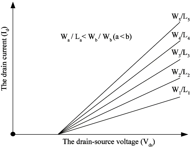
(a) different W/L
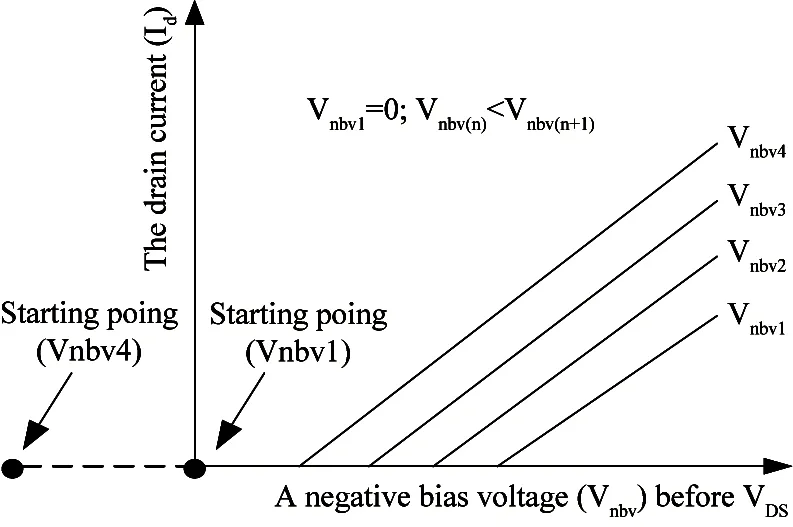
(b) differentVdcFig.2 MOSFET transmission characteristic curves with
Twographsaboveshowthatcombiningthetwocurvescanresultinaparallelcombinationlinearcurve.Finally,thepredistortionsignalisgeneratedusingmultiplecontrols,asshowninFig.3:
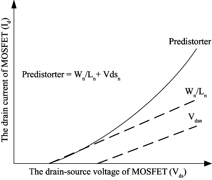
Fig.3 Predistortion characteristic curves schematic diagram of MOSFET parallel combination
2 Proposed analog predistortion topology
2.1 Fundamentals of the analog predistorter
Fig.4 is the schematic diagram of the N class current output array circuit. VMODE is the input node of modulation voltage, which controls the output current by transmitting the signal from VMODE to the gate of transistors MN1-MNn through the RC high-pass network. Meanwhile, bias voltage (Vbias1-Vbiasn) controls the gate voltage of MN1-MNn and switch voltage (Switch1- Switchn) controls the on/off of switch transistor MNS1- MNSn.
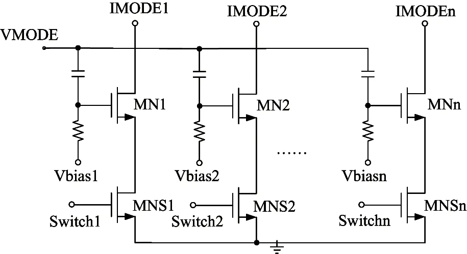
Fig.4 Schematic diagram of current output array circuit
As shown in Fig.5, the core component of the laser driver consists of a main amplifier and an auxiliary amplifier. To provide the DC bias input signal and the laser modulation input signal, the laser driver circuit must have a “bias” current and a “modulation” current respectively. The main amplifier and auxiliary amplifier drive two groups that modulate the output current array and provide the input current of the laser driver. Furthermore, modulating the output array can realize predistortion through current parallel combination.
2.2 Design of main amplifier
The overall laser driver circuit with an analog predistortion function consists of a main circuit and an auxiliary circuit. The schematic of the main circuit is shown in Fig.6. VBIAS, IBIS200μA and IBIAS1mA connect the bias voltage output and current output of low noise bandgap reference bias circuits respectively. R1 and R2 provide 50 Ohm impedance matching and constitute DC insulated matching networks with C1 and C2. The buffer stage (M4~M7) reduces the load capacitance of the front stage, provides a great deal of voltage-controlled current and increases driving capability for the latter stage. The current mirror circuits (M6, M7 and M9 ) provide a bias current by mirror amplifying the current generated by the input node IBIAS200μA to the buffer stage. For providing the linear characteristic of the circuit, the main amplifier (M1~M3, R3 and R4) are chosen as large-scale devices that provide large bandwidth with linear resistance. The current mirror circuits (M3, M8) provide bias current by mirror amplifying the current generated from input node IBIAS1mA to the amplifier. The high-pass network of the main amplifier (C3, R6, C4, and R5) transmits the AC modulation voltage to the gate of DC bias voltage. M10~M13 constitutes the current modulating output array of the main circuit.

Fig.6 Main circuit of the analog predistorter
IMODBIAS_A provides a variety of DC bias for the current modulating output array to control the threshold voltage of the array and achieve the output characteristics of the parallel combination. SWITCH_A<1> and SWTCH_A<0> provide the switch voltage for the current modulating output array to control the binary switch on/off and complete the effort of adjusting the output slope. IDCBIAS, SWITCHDC<1> and SWITCHDC<0> provide DC bias and switch voltage for the DC current output arrays respectively. The auxiliary circuit has the same structure as the main circuit except for the DC current output array.
2.3 Design of bandgap reference bias circuits
The noise of an optical communication system is minimal for meeting a high speed environment. The noise of a drive circuit and the ability for resisting the power interruption are restricted by a bandgap reference bias circuit. Therefore, realizing a low noise, high PSRR CMOS bandgap reference bias circuit can greatly enhance the performance of the entire laser driver circuit.
Fig.7 shows the low-noise bandgap reference bias circuit. The circuit design consists of five main parts: a negative temperature coefficient current mirror circuit, a positive temperature coefficient, a bias voltage output circuit, a bias current voltage output circuit and a noise suppression circuit.
The bias voltage output circuit adds the current mirror circuit of the positive temperature coefficient and negative temperature coefficient and turns it into the temperature- independent current and flow linear resistors R5 to convert voltage. Meanwhile, MN8 connects the form of capacitance to filter out AC interference and stabilize the output stage. The key idea of the noise suppression current mirror circuit is to utilize the difference of small signal characteristics between resistance and MOS to suppress AC noise while mirroring DC.

Fig.7 Low noise bandgap reference bias circuit
3 Implementation and experimental results
To support data transfer rates up to 1Gbps, IMT-Advanced choses 450~470MHz, 698~806MHz, 2.3~2.4GHz and 3.4~3.6GHz as the four frequency bands of the IMT-Advanced systems. To distinguish four-channel MIMO signals from photoelectric conversion modules, BBU (base band unit) + RRU (remote radio unit) are adopted to convert the signal to four tentatively identified intermediate frequencies (IF): 1.1GHz, 1.3GHz, 1.5GHz and 1.7GHz.
The rationale behind this method is to use the photoelectric conversion module, which has the 1~2GHz work dynamic range. Moreover, this method can distinguish signals by adopting a different IF wave carrier.
The design is fabricated in UMC 0.18μm CMOS technology and simulation is carried out in the Cadence Spectre environment. Simulation waveforms are shown in Figs8~10.

Fig.8 Simulation of temperature characteristics
The measurement results of the temperature characteristics are represented in Fig.8. The change of reference voltage is 5mV in the measurement range of -40℃ to 100℃.
As Fig.9 shows the entire circuit has a -3dB bandwidth from 250MHz to 2.4GHz and a gain of 13.3dB. Because the circuit works in the band of 1-2GHz after BBU+RRU in RoF, thus the bandwidth can meet the requirement of the design target.

Fig.9 Simulation of entire circuit for AC response
As shown in Fig.10, a 2G transient source is used for simulation and the maximum value of output voltage is 1.42V, the minimum is 1V, and the two curve intersection point voltage is 1.17V. Because the gain in output signal approximates high potential over low potential, the circuit meets the predistortion nonlinear requirements.
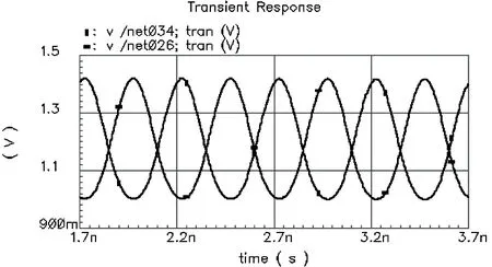
Fig.10 Simulation of transient waveform
The chip micrograph of the laser driver is shown in Fig.11. The left part of the layout is the bandgap reference and the right part is the laser driver circuit with the analog predistortion linearizer. The chip size is 1424μm×912μm including all AC and DC bond pads.
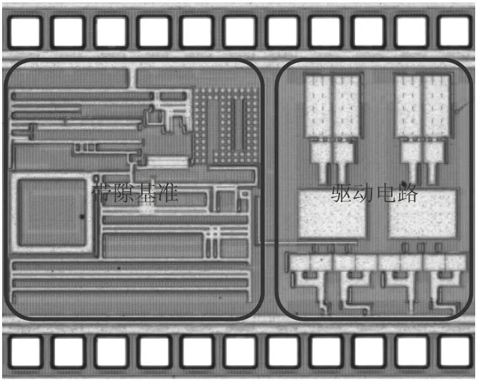
Fig.11 Chip micrograph of the proposed laser driver
Fig.12 shows the measured S21 parameters of the laser driver and reveals that the chip can work at a band-pass from 1~2.2GHz. Compared to the simulated result in Fig.9, the low frequency gain drops faster than simulated, which is possibly due to EM radiation loss, silicon substrate loss and process variations.

Fig.12 Measured S21 parameters of the laser driver
Fig.13 shows the result of the measured transient response, the waveform clearly shows that the gain of output signal in high potential is larger than that in low potential. Compared to the simulated result in Fig.10, the potential difference is smaller than simulated, which is possibly due to the inaccurate noise model, additional parasitic elements and substrate noise losses factored in simulation.

Fig.13 Measured transient response of the laser driver
Fig.14 shows the measured power spectrum densities (PSDs) of the laser driver circuit using a two-tone test. Fig.14(a) shows the PSDs of the laser driver without the analog predistorter and the IIP3 of the circuit is 1.38dBm. Fig.14(b) shows the PSDs of the laser driver with analog predistorter respectively and the IIP3 of the circuit is 6.29dBm. Thus, by inserting the analog predistorter module, the linearity of the circuit has improved obviously.

Fig.14 Measured PSDs of the laser driver
4 Conclusions
A novel tunable analog predistortion method for an integrated laser driver circuit is proposed. The slopes and flexion points of the predistortion module output transmission characteristic curve can be easily controlled by setting different W/L and bias voltage. The core circuit is fabricated using a standard 0.18μm CMOS technology. The measured circuit performance approximates to design specifications. The chip works well at a band-pass that ranges from 1GHz to 2.2GHz and consumes only 15mA DC current. As transient analysis demonstrated, the circuit has good nonlinear compensation effect and two-tone tests have shown that IIP3 of the entire circuit is improved by 4.91dB.
[1] Huang Y Y, Woo W, Jeon H, et al. Compact wideband linear CMOS variable gain amplifier for analog-predistortion power amplifiers.IEEETransactionsonMicrowaveTheoryandTechniques, 2012, 60 (1): 68-76
[2] Fang X H, Wu G A, Zhai Y, et al. A lumped-element analog predistorter for VHF application. In: Proceedings of International Symposium on Signals Systems and Electronics, Nanjing, China, 2010. 17-20
[3] Cho K J, Kim J H, Stapleton S P. A highly efficient Doherty feedforward linear power amplifier for W-CDMA base-station applications.IEEETransactionsonMicrowaveTheoryandTechniques, 2005, 53(1): 292-300
[4] Sun X L, Cheung S W, Yuk T I. A 5th-order analog predistorter for NADC system. In: IEEE International Conference on Communication Systems, Singapore, 2010. 19-22
[5] Jang S, Park B, Jung J H. Analog predistortion technique in remodulation based radio over high-speed access network for improving sensitivity. In: International Topical Meeting on Microwave Photonics, Singapore, 2011. 339-342
[6] Seo M, Kim K, Kim M, et al. Ultra broadband linear power amplifier using a frequency selective analog predistorter.IEEETransactionsonCircuitsandSystems. 2011, 58 (5): 264-268
[7] Roselli L, Borgioni V, Palazzari V, et al. An active cuber circuit for power amplifier analog predistortion. In: Proceedings of the 33rd European Microwave Conference, , Munich, Germany, 2003. 1219-1222
[8] Rezaei S, Hashmi M S, Dehlaghi B, et al. A systematic methodology to design analog predistortion linearizer for dual inflection power amplifiers. In: IEEE Microwave Symposium Digest, Baltimore, America, 2011. 1-4
[9] Lee Y S, Lee M W, Kam S H, et al. A transistor-based analog predistorter with unequal delays for memory compensation.IEEEMicrowaveandWirelessComponentsLetters, 2009,19 (11): 743-745
[10] Lee Y S, Lee M W, Jeong Y H. A wideband analog predistortion power amplifier with multi branch nonlinear path for memory effect compensation.IEEEMicrowaveandWirelessComponentsLetters, 2009, 19 (7): 476-478
[11] Li J H, Mao L H, Xie S, et al. A laser driver with analog pre-distortion technique for radio-over-fiber system. In: Proceedings of the 8th International Conference on Wireless Communications, Networking and Mobile Computing, Shanghai, China, 2012. 1-4
Song Qiwei, born in 1987. He received his B.S. degree from the PLA Information Engineering University in 2009. He also received his M.S. degree from GuiZhou University in 2012. He is currently working toward the Ph.D. Degree at the School of Electronic Information Engineering, Tianjin University. His research interests focuses on devices and broadband IC for optical communications.
10.3772/j.issn.1006-6748.2015.01.013
*Supported by the National Natural Science Foundation of China (No. 61036002).
*To whom correspondence should be addressed. E-mail: sqw6307@126.comReceived on Oct. 15, 2013
杂志排行

High Technology Letters的其它文章
- Research on assessing compression quality taking into account the space-borne remote sensing images*
- Filtered-beam-search-based approach for operating theatre scheduling*
- Exploiting PLSA model and conditional random field for refining image annotation*
- Maneuvering target tracking algorithm based on cubature Kalman filter with observation iterated update*
- Retrieval and analysis of sea surface air temperature and relative humidity*
- Data organization and management of mine typical object spectral libraries*