Preparation of Cu(In,Al)(Se,S)2Thin Films by Low-Cost Non-vacuum Hybrid Process
2015-01-20ZhofnLiuWeiXiChenchenYunPifengLuo
Zho-fn Liu,Wei Xi,Chen-chen Yun,Pi-feng Luo∗
a.Department of Materials Science and Engineering,Hefei University of Technology,Hefei 230009, China
b.CAS Key Laboratory of Materials for Energy Conversion,University of Science and Technology of China,Hefei 230026,China
(Dated:Received on February 3,2015;Accepted on July 5,2015)
Preparation of Cu(In,Al)(Se,S)2Thin Films by Low-Cost Non-vacuum Hybrid Process
Zhao-fan Liua,Wei Xiaa,Chen-chen Yuanb,Pai-feng Luoa∗
a.Department of Materials Science and Engineering,Hefei University of Technology,Hefei 230009, China
b.CAS Key Laboratory of Materials for Energy Conversion,University of Science and Technology of China,Hefei 230026,China
(Dated:Received on February 3,2015;Accepted on July 5,2015)
Cu(In,Al)(Se,S)2thin films were successfully obtained through a simple low-cost nonvacuum process.The Cu(In,Al)Se2raw material powder was firstly synthesized by a traditional solvothermal route.Then,the precursor coatings were prepared by drop-coating Cu(In,Al)Se2slurry.Finally,the Cu(In,Al)Se2and Cu(In,Al)(Se,S)2films were achieved by the selenization and/or sulfuration process.Through X-ray diffraction(XRD),scanning electron microscope,X-ray fluorescence,and absorption spectroscopy measurement,it was found that all the films show the single chalcopyrite phase structure and have the preferred (112)orientation.Meanwhile,after substituting selenium by sulfur,the main XRD peaks shift to higher 2θdegrees and the porous films become more compact.The energy band gap also increases to a suitable range for light absorption from 1.21 eV to 1.33 eV,which indicates that the additional sulfuration process is much more favorable for improving the quality of Cu(In,Al)(Se,S)2films.
Non-vacuum,Solvothermal,X-ray diffraction,Sulfuration
I.INTRODUCTION
Currently,CuInSe2and related materials have been broadly considered as the fascinating absorber layers for applications in thin-film solar cells due to their suitable energy band gap(Eg),high absorption coefficient and good stability[1−4].However,the relative narrow Eg(1.0 eV)of CuInSe2films still need to be optimized in order to meet the demand for high efficient photovoltaic devices.Thus current strategy of increasing Egis usually employing groups III and/or VI elements to alloy with CuInSe2chalcopyrite.As such,a wide band gap range from 1.0 eV to 1.7 eV can be tuned by adjusting the Ga/(In+Ga)or S/(Se+S)ratio.Recently,the effect of gallium or sulfur addition on the increased Eghas been reported[5−7].Unfortunately,after alloying with Ga,the power conversion efficiency of CuInGaSe2solar cells will be limited by the degradation of electronic properties when its Egis larger than 1.3 eV[8,9]. Therefore,much attention has been focused on the development of the alternate alloy materials replacing the traditional element Ga in CuInGaSe2films.
It is well known that Al is a cheap and abundant element compared with expensive metal material Ga. More importantly,it requires relative smaller alloy amounts than that of Ga alloy to achieve a comparable band gap[10−13].Cu(In,Al)Se2material with a wide Egranging from 1.04 eV to 2.67 eV has been recognized as an ideal alternative to the common CuInGaSe2absorber layer.The experimental manipulation of using stable aluminide is also much more convenient than that of moisture-absorbing gallium-based compound.Intriguingly,the deep defect band found in CuInGaSe2films usually acts as the electron-hole recombination center,which is not observed in Cu(In,Al)Se2material[14,15].In terms of its excellent photoelectric properties,Cu(In,Al)Se2materials have triggered a strong research interest,and so far the highest efficiency of 16.9%for Cu(In,Al)Se2solar cells was successfully achieved[16].Up to now,many vacuum techniques,such as co-evaporation[10,16]and sputtering [12,15],have been employed to deposit Cu(In,Al)Se2films.However,these methods still need expensive equipment investment and complicated manufacture process.As a result,more research and development on simple deposition techniques is necessary for the breakthrough of fabrication of Cu(In,Al)Se2absorber layers.
Basically,the low-cost non-vacuum techniques are inherently suitable for large-scale applications according to the established coating industries[17].Lately,combustion approach and direct reduction of the oxide precursors are continuously developed by our group to fabricate Cu(In,Al)S2layers[18,19].Meanwhile,Kavithaalso present a chemical bath deposition technique to grow Cu(In,Al)Se2films[20].But those chemicalmethods need complex reaction process and encounter incomplete conversions,which leads to the poor reproducibility and a large variation on the films performance,and is also not suitable for large-scale applications.Therefore,concerning the fabrication techniques of nanoparticles,solvothermal route has the advantage of being a simple and inexpensive low-temperature process[21−23].But to the best of our knowledge,so far there is no report of preparing Cu(In,Al)Se2films by the solvothermal route and drop-coating method,followed by a selenization and sulfuration sequential process.Hence,an attempt has been made to prepare Cu(In,Al)Se2coatings using this simple non-vacuum method.At the same time,many CuInGaSe2companies employ additional sulfuration process to improve the quality and tune the band gap of chalcopyrite films. In this regard,here Cu(In,Al)(Se,S)2films are consecutively prepared by a solvothermal route,drop-coating, selenization,and sulfuration process.The structure and opticalproperties of Cu(In,Al)Se2and Cu(In,Al)(Se,S)2films were both investigated.
II.EXPERIMENTS
The Cu(In,Al)(Se,S)2films were prepared by a solvothermal route,drop-coating,and selenization/sulfuration hybrid process.First,the Cu(In,Al)Se2precursor powder was synthesized by the traditional solvothermal route.In a typical synthesis,the required amount of CuSO4·5H2O(0.323 g), In2(SO4)3(0.256 g),AlCl3(0.040 g),and Se(0.205 g) powder was loaded into a 50 mL Teflon lined autoclave, which was then filled with anhydrous ethylenediamine up to 80%of the total volume.The sealed autoclave was maintained at a reaction temperature 180◦C for 18 h and then cooled down to room temperature.The precipitate was centrifuged and washed with distilled water and ethanol for several times.The particles was filtered off and dried at 60◦C for 6 h and milled at ambient temperature in an agate mortar for 3 h.Second, suitable thickening agent ethyl cellulose and dispersant polyethyleneglycol were selected to formulate the slurry with suitable viscosity.The precursor coatings were deposited via drop-coating the precursor slurry and heated to remove solvent and burn organic additives. Finally,the pretreatment films were selenized and/or sulfurated in a two-zone furnace with a quasi-closed quartz crucible under a vacuum furnace of 3×10⁻²Pa. In order to avoid the harmful oxygen,Argon was used to wash the chamber for three times.The selenization and/or sulfuration process was performed at 500◦C for 1 h with selenium and/or sulfur vapor evaporated at 300◦C,respectively.

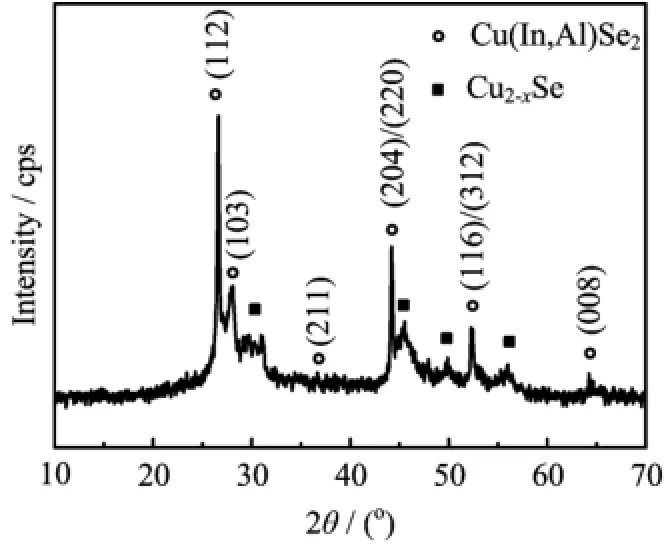
FIG.1 The XRD pattern of the Cu(In,Al)Se2precursor powder.
The phase composition and the crystal structure of the films were identified by X-ray diffraction(XRD) method(D/Max-rA).The morphology of the films was observed on a field emission scanning electron microscope(FESEM,JEOL-JSM-6700F).The composition of films was measured by X-ray fluorescence(XRF, SHIMADZU,VF-320)method.The optical absorption spectrum was recorded on a UV-Vis-365-type spectrophotometer in range of 300−1500 nm.
III.RESULTS AND DISCUSSION
A.Preparation of Cu(In,Al)Se2precursor powder
Figure 1 shows the XRD patterns of Cu(In,Al)Se2precursor powder by the solvothermal route.As shown in Fig.1,Cu(In,Al)Se2films exhibit the chalcopyrite phase oriented along(112)direction,and the other prominent peaks(204)/(220)and(116)/(312)are also observed.The weak orientations such as(103),(211), and(008)are also detected in the XRD pattern,which usually can’t be shown in the sphalerite phase structure. So it can be concluded that the made Cu(In,Al)Se2films belong to the chalcopyrite phase structure.Meanwhile, the secondary Cu2−xSe phase shown in the XRD pattern must be caused by the Cu-rich composition,which has been discussed on the synthesis of CuInSe2films by solvothermal route[22,23].
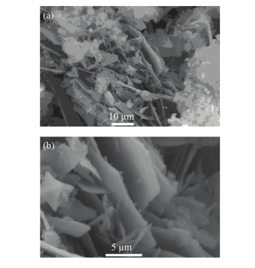
The planar SEM micrograph of the Cu(In,Al)Se2precursor powder by solvothermal route with different magnifications is shown in Fig.2.So many plate-like particles like stacked knives are obtained from the reaction in the ethylenediamine solvent.The crystal growth of Cu(In,Al)Se2powder is very sufficient and the grain size attains tens of micron level.And the secondary Cu2−xSe phase with anomalistic morphology is also observed from the SEM,which wellaccords with the result of XRD.The solution-liquid-solid mechanism for the one-dimensional growth can explain this phenomenon [23,24],which is very similar to the growth mechanism of CuInSe2films[22].

FIG.2 The planar SEM micrograph of the Cu(In,Al)Se2precursor powder.

TABLE I The composition of the Cu(In,Al)Se2powder, Cu(In,Al)Se2,and Cu(In,Al)(Se,S)2films determined by XRF.
The composition of the Cu(In,Al)Se2precursor powder was accurately determined by XRF,the results are shown in Table I.The ratio of Cu:In:Al:Se= 27.82:18.25:5.47:48.46 is close to 1:0.77:0.23:2,which is consistent with that in the raw materials and shows slightly Cu-rich powder.As mentioned in the XRD and SEM,the results may be attributed to the existence of the secondary Cu2−xSe phase.The data reported here suggest that typical near stoichiometric,but a little Cu-rich Cu(In,Al)Se2precursor powder was synthesized by solvothermal route in this work.
B.Selenization and/or sulfuration of Cu(In,Al)Se2precursor powder

FIG.3 The XRD patterns of(a)Cu(In,Al)Se2films and (b)Cu(In,Al)(Se,S)2films.

FIG.4 The expanded view of the(112)diffraction peak of the(a)Cu(In,Al)Se2and(b)Cu(In,Al)(Se,S)2films.
After selenization and/or sulfuration of the Cu(In,Al)Se2precursor powder,the XRD patterns of Cu(In,Al)Se2films and Cu(In,Al)(Se,S)2films are shown in Fig.3,respectively.Both the Cu(In,Al)Se2films and the Cu(In,Al)(Se,S)2films show the single chalcopyrite phase structure and have the preferred (112)orientation,no other impurity peaks are found. The existing secondary Cu2−xSe phase completely converts to pure chalcopyrite phase after selenization and/or sulfuraition at 500◦C for 1 h,which has been proven by many groups[22,25].Figure 4 shows the expanded view of the(112)diffraction peak of Cu(In,Al)Se2and Cu(In,Al)(Se,S)2films.The(112) peak of Cu(In,Al)(Se,S)2films shows a systematic shift toward higher 2θdegrees after the additional sulfuration process.The shift in the diffraction peak is expected due to decrease in the unit cell lattice parameters with incorporating sulfur,which has smaller atomic size relative to selenium.From thermodynamic calculations,according to the thermodynamic constants of individual species from literature[26], the free energy of reaction for Cu(In,Al)Se2(s)+S2(g) =Cu(In,Al)(Se,S)2(s)+Se2(g)at 800 K is very close to zero.Therefore,the reaction may be driven in either direction by adjusting the vapor pressure of selenium and sulfur.In this case,the driving mechanism for the replacement of selenium in Cu(In,Al)Se2by sulfur is motivated by the elevated partial pressure of sulfur vapor.So,in accordance with the result of XRD measurement,single chalcopyrite phase is obtained in this work,which means the above reaction occurs and sulfur partially substitutes selenium in the chalcopyrite films.

FIG.5 The planar(a)and cross-sectional(b)SEM micrograph of Cu(In,Al)Se2films.

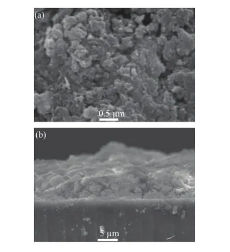
FIG.6 The planar(a)and cross-sectional(b)SEM micrograph of Cu(In,Al)(Se,S)2films.
The planar and cross-sectional SEM micrograph of Cu(In,Al)Se2films is shown in Fig.5.After milling the plate-like particles and selenization process,a porous Cu(In,Al)Se2films with gain size below 300 nm were obtained.This is well explained by the following mechanism:from the thermodynamic aspect, Cu(In,Al)Se2powder with chalcopyrite phase synthesized by solvothermal route is very stable,with a very high melting point around 1000◦C.The reaction mechanism must be the gas-solid route,but not the expected gas-liquid mode.So it displays a porous layer with small grains due to the shortage of the reaction force of the selenium vapor.Figure 6 shows the planar and cross-sectional SEM micrograph of Cu(In,Al)(Se,S)2films.From the images,we can see that dense Cu(In,Al)(Se,S)2grains with larger size attaining micron levels,which is a very important feature for high quality absorber layer,were obtained on the glass substrates after the additional sulfuration treatment.In Guo’s point of view,when sulfur was replaced by selenium,it would cause volume expansion and dense coatings were obtained[27].Interestingly,comparing with Fig.5 with Fig.6,we may also observe the densification phenomenon of the porous absorber layer when selenium is replaced by sulfur.As mentioned above, many CuInGaSe2companies,such as solar frontier and Taiwan Semiconductor Manufacturing Company,usually employ the additional sulfuration process to improve the quality and tune the band gap of chalcopyrite materials[28,29].
Table I also shows the compositions of the Cu(In,Al)-Se2and Cu(In,Al)(Se,S)2films determined by XRF. The ratio of Cu:(In+Al):Se=27.76:(18.04+5.28):48.92 in the Cu(In,Al)Se2films after selenization is close to 1:1:2,which is obviously in accordance with the stoichiometric ratio and shows little Se-poor.In general, the Se-poor films show the n-type conduction and can not be used in the preparing photovoltaic devices.So the main point is to increase the content of selenium or sulfur,and to be a(Se+S)-rich films with p-type conduction.On the contrary,it is found that the ratio of Cu:(In+Al):(Se+S)=25.59:(17.98+5.16):(10.25+41.02) in the Cu(In,Al)(Se,S)2films after sulfuration is very close to 1:1:2.The sulfur element replaces 80%of selenium element in the Cu(In,Al)(Se,S)2films,and it shows little(Se+S)-rich.So typical near stoichiometric little(Se+S)-rich Cu(In,Al)(Se,S)2films are obtained in this work.
Figure 7 shows the photon energy dependence of the absorption coefficient of Cu(In,Al)Se2films and Cu(In,Al)(Se,S)2films.Both of them have a good optical property with high absorption coefficient exceeding 105cm−1.In general,chalcopyrite materials are directgap semiconductors with the valence-band maximum and conduction-band minimum at k=0.According to the formula Eg=hν=1240/λ,we can calculate the band gap Eg.So the midpoint of the absorption edge near the arrow’s location marked in the figture is selected to assess the Egvalue.The wavelength valueλ=1024 nm for Cu(In,Al)Se2films corresponds to the band gap of 1.21 eV,andλ=932 nm for Cu(In,Al)(Se,S)2films is about 1.33 eV.The similar band gap Eg=1.25 eV of CuInO.75AlO.25Se2films is also reported by Paulson et al.[9].From our results of XRF and absorption spectroscopy measurement,a bang gap of 1.21 eV for the prepared CuInO.77AlO.23Se2films was obtained in this work.Both the band gaps of Cu(In,Al)Se2and Cu(In,Al)(Se,S)2films are much larger than that of CuInSe2films(Eg=1.04 eV)[30].So the Egcan be increased to match the solar spectrum for higher efficiency by alloying aluminum.Meanwhile,the incorporation of sulfur also can further improve the band gap about 0.12 eV.Therefore,we can tune the band gap through controlling the S:(S+Se)and/or the Al:(Al+In)ratios by changing the sulfuration time.

FIG.7 The photon energy(hν)dependence of the absorption coefficient(α)for Cu(In,Al)Se2and Cu(In,Al)(Se,S)2films.λ=1024 nm for Cu(In,Al)Se2films corresponds to the band gap of 1.21 eV(solid line),andλ=932 nm for Cu(In,Al)(Se,S)2films is about 1.33 eV(dashed line).The arrow means the shift of band gaps.
IV.CONCLUSION
Cu(In,Al)Se2and Cu(In,Al)(Se,S)2films have been prepared by using a simple low-cost non-vacuum process in this work,which indicates a promising way for the application in thin-film solar cells.Employing air-open solvothermal route,combining with traditional drop-coating,selenization/sulfuration process, (112)orientated Cu(In,Al)(Se,S)2films with single chalcopyrite phase are obtained here.Further research finds that the additional sulfuration process can effectively improve the quality and increase the Egof the chalcopyrite coatings,which is expected to be applied in the gradient band gap thin-film solar cells.
V.ACKNOWLEDGMENTS
This work was financially supported by the National Natural Science Foundation of China(No.51302058 and No.U1532140),the Natural Science Foundation of Anhui Province(No.JZ2015AKZR0031),and the Opening Project of CAS Key Laboratory of Materials for Energy Conversion at University of Science and Technology of China.
[1]W.Li,Z.Pan,and X.Zhong,J.Mater.Chem.A 3, 1649(2015).
[2]A.Chirila,P.Reinhard,F.Pianezzi,P.Bloesch,A. R.Uhl,C.Fella,L.Kranz,D.Keller,C.Gretener, H.Hagendorfer,D.Jaeger,R.Erni,S.Nishiwaki,S. Buecheler,and A.N.Tiwari,Nat.Mater.12,1107 (2013).
[3]H.Mcdaniel,A.Y.Koposov,S.Draguta,N.S. Makarov,J.M.Pietryga,and V.I.Klimov,J.Phys. Chem.C 118,16987(2014).
[5]K.Zhang,C.Yang,L.Yin,Z.Liu,Q.Song,H.Luo, Z.Xiong,M.Xu,and X.Xiao,Sol.Energy Mater.Sol. Cells 120,253(2014).
[6]I.Repins,M.Contreras,B.Egaas,C.DeHart,J.Scharf, C.Perkins,B.To,and R.Noufi,Prog.Photovolt.:Res. Appl.16,235(2008).
[7]J.Palm,V.Probst,W.Stetter,R.Toelle,S.Visbeck,H. Calwer,T.Niesen,H.Vogt,O.Hernandez,M.Wendl, and F.H.Karg,Thin Solid Films 451/452,544(2004).
[8]V.Ranjan,T.Begou,S.Little,R.W.Collins,and S. Marsillac,Prog.Photovoltaics 22,77(2014).
[9]U.Rau,M.Schmidt,A.Jasenek,G.Hanna,and H. Schock,Sol.Energy Mater.Sol.Cells 67,137(2001).
[10]P.Paulson,M.Haimbodi,S.Marsillac,R.Birkmire, and W.Shafarman,J.Appl.Phys.91,10153(2002).
[11]U.Parihar,K.Sreenivas,J.R.Ray,C.J.Panchal,N. Padha,and B.Rehani,Mater.Chem.Phys.139,270 (2013).
[12]D.Perng,J.Chen,and C.Wu,Sol.Energy Mater.Sol. Cells 95,257(2011).
[13]K.G.Deepa,N.L.Shruthi,M.A.Sunil,and J.Nagaraju,Thin Solid Films 551,1(2014).
[14]J.Heath,J.Cohen,and W.Shafarman,Mater.Res. Soc.Symp.Proc.763,441(2003).
[15]D.Dwyer,I.Repins,H.Efstathiadis,and P.Haldar, Sol.Energy Mater.Sol.Cells 94,598(2010).
[16]S.Marsillac,P.D.Paulson,M.Haimbodi,R.Birkmire, and W.Shafarman,Appl.Phys.Lett.81,1350(2002).
[17]C.Hibberd,E.Chassaing,W.Liu,D.Mitzi,D.Lincot, and A.Tiwari,Prog.Photovolt:Res.Appl.18,434 (2010).
[18]P.Luo,R.Zuo,and L.Chen,Sol.Energy Mater.Sol. Cells 94,1146(2010).
[19]P.Luo,P.Yu,R.Zuo,J.Jin,Y.Xu,Y.Ding,and J. Song,Scripta Mater.64,422(2011).
[20]B.Kavitha and M.Dhanam,Superlattices Microstruct. 51,301(2012).
[21]J.Park,J.Alloys Compd.629,162(2015).
[22]P.Luo,P.Yu,R.Zuo,J.Jin,Y.Ding,J.Song,and Y. Chen,Phy.B 405,3294(2010).
[23]Y.Chun,K.Kim,and K.Yoon,Thin Solid Films 480, 46(2005).
[24]T.Trentler,K.Hickman,S.Goel,A.Viano,P.Gibbons, and W.Buhro,Science 207,1791(1995).
[25]P.Luo,Z.Liu,Y.Ding,and J.Cheng,J.Power Sources 274,22(2015).
[26]D.Cahen and R.Noufi,J.Phys.Chem.Solids 53,991 (1992).
[27]Q.Guo,G.Ford,H.Hillhouse,and R.Agrawal,Nano Lett.9,3060(2009).
[28]P.Reinhard,S.Buecheler,and A.N.Tiwari,Sol.Energy Mater.Sol.Cells 119,287(2013).
[29]K.Kushiya,Sol.Energy Mater.Sol.Cells 122,309 (2014).
[30]J.Lauth,J.Marbach,A.Meyer,S.Dogan,C.Klinke, A.Kornowski,and H.Weller,Adv.Funct.Mater.24, 1081(2014).
.Kuo,H.Tsai,A.Huang,and W.Pan,Appl.Energy
10.1016/j.apenergy.2015.04.002.
∗Author to whom correspondence should be addressed.E-mail: lpfeng@hfut.edu.cn,Tel.:+86-551-62904566
杂志排行
CHINESE JOURNAL OF CHEMICAL PHYSICS的其它文章
- Visualization of Melting of Antiferromagnetic Insulator Phase in Phase-Separated Manganite Film using Magnetic Force Microscopy
- Oxidation of Anatase TiO2(001)(1×4)Surface
- One-Dimensional Scanning of Electronic Wavefunction in Carbon Nanotubes by Molecular Encapsulation
- Chemical Empiricism 2.0 at Age of Big Data:Large-scale Prediction of Reaction Pathways Based on Bond Dissociation Energies
- First-Principles Study of La Doping Effects on the Electronic Structures and Photocatalytic Properties of Anatase TiO2
- Reconstruction of Smoke Plume Concentration Peaks Based on Modified MAX-DOAS Tomography
