Analysis for Transm ission of Com posite Structure w ith Graphene Using Equivalent Circuit M odel*
2014-05-05XuBingzheng许秉正GuChangqing顾长青LiZhuo李茁NiuZhenyi牛臻弋
Xu Bingzheng(许秉正),Gu Changqing(顾长青),Li Zhuo(李茁),Niu Zhenyi(牛臻弋)
College of Electronic and Information Engineering,Nanjing University of Aeronautics and Astronautics,Nanjing,210016,P.R.China
1 Introduction
The applications of periodic structures to control electromagnetic wave propagation have been attracted in various research fields for centuries[1].Many of papers have been published for exploring the theoretical challengeswith the description of the first diffraction grating[2-7].Possible applications of periodic structures include design of frequency selective surfaces(e.g.antenna radome,absorber)[2],artificial high-impedance surfaces(HIS)[3],and photonic band-gap structures(PBG)[4].The periodic structure relies usually on the uses of commercial full-wave electromagnetic solvers,which consume considerable time and computational resources for accurate results.Fortunately,themodeling of periodic structures in the sub-diffraction regime can be carry through very simple models based on the equivalent circuit method(ECM)[5-7].For instance,simple and accurate analytical formulas are introduced for the reflection of the high-impedance surfaces comprising metal strips or patches over ground planes[5].In addition,the transmissivity of electromagnetic waves through stacked two-dimensional printed periodic arrays of square conducting patches is studied and an analytical circuitlike model is used for the analysis[6].Transmission through two-dimensional(2D)periodic metallic meshes are also discussed recently[7].However,to the best of our knowledge,circuitmethods of the composite structures with both patch and mesh layers have rarely been studied yet.It is interesting to consider transmission through composite structure by an efficient equivalent circuit approach.
On the other hand,graphene has attracted great attention for potential applications in various branches of engineering due to its predominant electronic transport properties[8].One novel area where the property of graphenemay be influential is the dynamic control of the applied bias voltage[9].And graphene sheet can be used to realize the concept of″cloaking by a surface″in the far-infrared and terahertz regime[8].Furthermore,an analyticalmodel is presented for the analysis ofmultilayer wiremedia loaded with 2D HIS such as graphenemonolayer on the thin material terminations,characterized in general by the complex surface conductivity,applied to wideband absorbers[10].The use of periodic graphenemeta-surfaces to dynamically control the electromagnetic wave reflection,absorption,or polarization was reported in recent times[11].For the complexity of the conductivity of graphene,it is necessary to discuss the simple equivalent impedance surfacemodel.
In this paper,the formalism of the equivalent model is presented for the analysis of the transmission characteristics of the multilayer structure with graphene and metal sheets.It is shown that the electronic gating of a graphene monolayer allows one to change transmission of electromagnetic waves of the structure.The results obtained using the analytical model are validated against computationally intensive finite element commercial electromagnetic solver.
2 Unit Cell M odel of Com posite Stacked Grids and Patches
In the infrared and microwave range,graphene monolayer can be described as a complex-valued surface conductivity[8,9]

whereω is the radian frequency of the plane wave,Γ a phenomenological scattering rate,which is assumed to be independent of energy,T the room temperature,μcthe chemical potential related to the electrostatic biasing,which quantifies the electronic transport properties.Throughout thiswork,we assume T=300 K,Γ =0.43 meV,which corresponds a mean-free path of several hundred nanometers,and set 0.0 —1.0 eV as the chemical potential scope for discussion.In general,graphene layer can reside on substrate,such as a silicon dioxide(SiO2)thin film with relative permittivity ε'=3.9 with the thickness of severalmicrometers.For the thin thickness,the silicon dioxide substrate can be ignored for our analysis.In order to tune the chemical potential of the whole graphene layer by electrostatic gating,graphene layer should be connected,that iswhy we consider2D graphene strips instead of isolated structure such like patch or cross arrays.
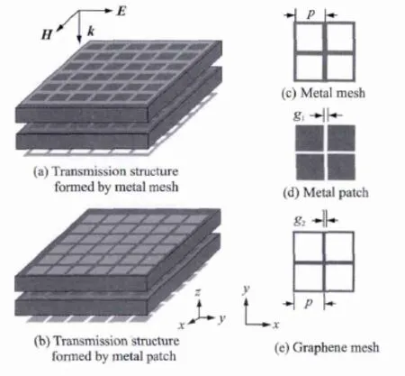
Fig.1 Configuration of transmission structure
Examples of themultilayer configuration analyzed are depicted in Fig.1,showing that the bilayer configuration is formed with differentmesh grids separated by commercially available dielectric (Roger 3210).The relative permittivity of the dielectric material isεd=10.2 ,and the loss tangent used in the analysis is tanδd≈ 0.003 ,the thickness of the each of the substrate is h=4 mm.The copper cladding with 18μm thicknessisplaced on the top and bottom layer,itisassumed thattheparametersofthemetallayerare the same.And graphene grids are placed between two dielectric slabswith a complex surface conductivity as a thin tunable resistive sheet.Although 6 × 6 unit cells along the x and y directions are shown in Figs.1(a,b),the structure is assumed infinite in the transverse directions.And the lattice constants of both the metallic and the graphene grids are p=2 mm,much smaller than the wavelength in the dielectric slabs at the operation frequency.And the width of the metal and graphene strips is g1=0.1 mm and g2=0.05 mm(see Figs.1(c,d,e)).For the symmetric of the structure,the structure is not sensitive to the polarization angle of the incidentelectromagnetic wave.When a uniform transverse plane electromagnetic wave incident to the structure,themodel of themetallic or graphene strips with sub-wavelength period and dimensions has been proposed for the transmission properties.
3 Analysis and Derivation of Equivalent Circuit M odel
Now consider a plane wave incident normally on the multilayer structure as shown in Fig.1.It is assumed that each dielectric layer is homogeneous and the wavelength in free space is larger than the period in the transverse direction of the structure under study.The appropriate equivalent circuit of the investigated structure in our simulation is depicted in Fig.2.The impedance Zdaccounts for the inductance of the thin dielectric slab and Z0represents the free space impedance,the expressions for those value of the propagation constants(β0for the air space andβdfor the dielectric region)and impedance for normal incidence are[5-7]

Fig.2 Equivalent circuit for the composite structure with sub-wavelength periodic elements
whereλis the incidencewavelength,μ0andε0are the permeability and permittivity in free space,respectively.The shunt impedances of the metal grids or patches in each layer can be expressed asThe lossy resistive sheetusing graphene is represented by impedance Zp.The size of the unit cell considered in our analysis is electrically small,approximate estimations for the grid or patch impedance based on the dynamic solution for some periodic structures(patch arrays,mesh grids,among others)are available in the literature.In the circuitmodel analysis,for g1≪p themetallic grids can be simply represented by a reactive loads Zgfor normal incidence[5]
where the ohmic losses can be neglected for the skin effect penetration depth is much smaller than the thickness of the metal mesh.Similarly,the metal patch grid behavesmainly as a capacitive load,and the analytical expressions for patch arrays can be obtained[5]

where ″csc″stands for the cosecant function and εeff=(εd+1)/2 stands for the equivalent relative permittivity for the patch located at the upper interface.According to the proposed model,the grid impedance of graphene strips can be obtained as follows
For simply,it can be equivalent to two terms:the first term represents conduction loss per period due to the presence of graphene,the second term is the approximate grid impedance of themesh array(similar to Eq.(4)).Once the impedance of the metallic or graphenemeshes is derived,the transmission coefficient of the structure is assessed as follows
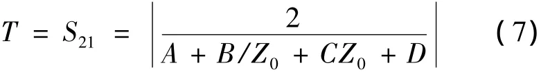
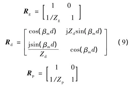
the terms A,B,C,D are the elements of the transmission linematrix of the composite structurewhich is evaluated as the product of the five cascaded matrices

where the transmission linematrix Rg,Rp,Rdcan be expressed as
In order to present a practical design of the structure,the predictions of ourmodelmust be checked against experimental and numerical results.The forthcoming section will give the numerical and analytic data.
4 Results and Discussion
The approximate circuit method here presented allows acquiring a valuable insight into the physical principles of the bilayer structure.The conductivity of graphene corresponds to the surface impedance of a graphenemonolayer Zgr=1/σgr[8],which behaves as a resistive surface due to the small values ofσgratmicrowave frequencies.Fig.3(a)illustrates the input(surface)impedance of the structure(Fig.1(a))with graphenemonolayer in different chemical potential.For uc=0 eV(no bias voltage is loading),the real part of the surface conductivity of graphene is equivalent to 3.23 mS,corresponding to 310 Ω,and for uc=1 eV,the real partof the surface conductivity is about 89.97 mS,corresponding to 11 Ω.For the high impedance the input impedance curve at the frequency range of 0—18 GHz has three high peaks.Apparently,this leads to good matching with the free space impedance at the range of the frequency.Similar simulation has occurred in Fig.3(b)which corresponds to the composite structure in Fig.1(b).Additionally,there is a transmission peak occurring at zero frequency for uc=0 eV.
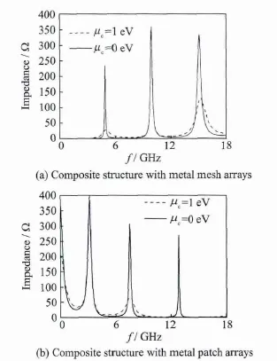
Fig.3 Input(surface)impedance with different chemical potential
In order to validate the effectiveness of the formulas,we present numerical values of the transmissivity(|T|2=|S21|2)of this structure computed with the full-wave results.The full-wave results are calculated by using the electromagnetic finite elements solver HFSS.The results shown in Fig.4 are obtained using different values of chemical potential for normal incidence with the following geometrical and material parameters of the structure in Fig.1(a).There is an agreement between numerical and analytical data from the Fig.4.When uc=0 eV ,the structure exhibit three high-transmission peaks with the resonance frequencies between 2 to 18 GHz.And the structure exhibits a low-pass filter behavior with strong ripples.When the bias voltage changes to 1 eV,only one peak(10 GHz)is found.The formula is applicable in different chemical potential from 0—1 eV.

Fig.4 Comparison between analytical and numerical results for transmissivity(|T|2)of structure in Fig.1(a).
Here we consider amultilayermetal patches and graphene meshes structure as shown in Fig.1(b).The structure is formed with metal identical patch arrays separated by dielectric slabs.Firstly,Fig.3(b)presents the real part of the input impedance of the structure.From Figs.5(a,b)it can be observed that the transmissivity behavior shows a passband stating from the zero frequency and up to a certain upper frequency.When graphene has no bias voltage,the high impedance surface impedance lead to three peaks at the range between 0—18 GHz.By decreasing the value of the surface impedance of graphene,the real part of input impedance curves changes with the second peaks transmission lost.And in Fig.5(b),the transmission coefficient of the structure have only two peakswhich obtained by the equivalent circuitmethod and HFSS.Again,the results obtained using the ECM are in good agreement with the HFSS results in any value of the bias voltage.

Fig.5 Comparison between analytical and numerical results for transmissivity(|T|2)of structure in Fig.1(b).
In the previous example,it has been shown that the ECM is convenient to study the characteristics of the transmission band.For this purpose,we apply the circuitmodel to analysis the transmission characteristics in structures formed by a large number of layers with graphene or metal mesh grids and dielectric slabs.Fig.6 shows the transmission characteristics of a ten-layer structure(graphene sheets biased with the same chemical potential)and all the peaks are within the characteristic frequency band.The structure is formed by a stack of six identicalmetalmesh grids and five graphene mesh grids printed on ten identical dielectric slabs.The substrate has the thickness of h=6 mm,p=5 mm,and g1=g2=0.15 mm.In Fig.6,it can be observed that the structure exhibits a series of band-pass regions separated by the band gaps,similar to the previous examples.The ECM is also applicable to the multilayer case.It should be noted that the bandpass and bandstop behavior is dependenton the geometrical andmaterial parameters of the dielectric slabs and graphene sheets,and the five numbers of transmission peaks of every bandpass regions correspond to the numbers of the graphene layers.
5 Conclusions

Fig.6 Transmission spectra obtained for ten dielectric slabs(five graphene mesh layer and six metal mesh layer)
Transmissivity of electromagnetic waves through stacked 2D dimensional periodic graphene/metal mesh or patch arrays is analyzed at microwave frequencies.The study has been carried using the transfer-matrix approach,and an independent verification has been provided with the computationally intensive finite element commercial electromagnetic solver.In the situation of the transmission bands and the bandgaps are accurately determined bymeans of the ECM.Themodel is valid in the case ofmulti-layers compute structure.In thiswork,we consider only normal incidence of electromagnetic waves,but the approach can be easily extended to an oblique incidence with the TE and TM reflection and transmission coefficients[6].The considered structures with graphenemay be useful in the design of tunable broadband planar filters at microwave frequencies.
[1] Rittenhouse D.Explanation of an optical deception[J].Transactions of the American Philosophical Society,1786,2:37-42.
[2] Costa F,Monorchio A.A frequency selective radome with wideband absorbing properties[J].Transactions on Antennas and Propagation,2012,60(6):2740-2746.
[3] Maci S,Kildal P S.Hard and soft surfaces realized by FSS printed on a grounded dielectric slab[C]∥Proseeding of Antennas and Propagations Society International Symposium.Siena,Italy:IEEE,2004:285-288.
[4] Yablonovitch E.Inhibited spontaneous emission in solid-state physics and electronics[J].Phy Rev Lett,1987,58(20):2059-2062.
[5] Luukkonen O,Simovski C,Granet G,et al.Simple and accurate analyticalmodel of planar grids and highimpedance surfaces comprising meta strips or patches[J].Transactions on Antennas and Propagation,2008,56(6):1624-1630.
[6] Kaipa C SR,Yakovlev A B,Medina F,et al.Transmission through stacked 2D periodic distribution of square conducting patches[J].Journal of Applied Physics,2012,112(3):033101.
[7] Costa F,Genovesi S,Monorchio A,et al.Circuitmodeling of the transmissivity of stacked two-dimensional metallic meshes[J].Optics Express,2010,18(13):13309-13320.
[8] Chen P Y,Alu A.Atomically thin surface cloak using graphene monolayers[J].ACS Nano,2011,5(7):5855-5863.
[9] Xu H J,Lu W B,Jiang Y,et al.Beam-scanning planar lens based on graphene[J].Applied Physics Letters,2012,100:051903.
[10] Padooru Y R,Yakovlev A B,Kaipa C SR,et al.New absorbing boundary conditions and analytical model for multilayeredmushroom-typemetamaterials:Applications to wideband absorbers[J].Transactions on Antenna Propagation,2012,60(12):5727-5742.
[11] Fallahi A,Perruisseau-Carrier J.Design of tunable biperiodic graphenemetasurfaces[J].Physical Review B,2012,86(19):195408.
猜你喜欢
杂志排行

Transactions of Nanjing University of Aeronautics and Astronautics的其它文章
- Experiment on Adiabatic Film Cooling Effectiveness in Front Zone of Effusion Cooling Configuration*
- Control System in M issiles for W hole-Trajectory-Controlled Trajectory Correction Projectile Based on DSP
- Panoram ic Imaging System Inspired by Insect Com pound Eyes*
- Geometric Covariance Modeling for Surface Variation of Compliant Parts Based on Hybrid Polynomial Approximation and Spectrum Analysis*
- Focus Reflective Shock Wave Interaction with Flame
- Fast SSED-MoM/FEM Analysis for Electromagnetic Scattering of Large-Scale Periodic Dielectric Structures*