一种米勒通路补偿的两级放大器
2013-12-30侯俊芳
侯俊芳
(天津轻工职业技术学院科研设备处,天津300350)
Miller compensation is the most commonly used frequency compensation technique of two-stage amplifiers.The compensation mechanism has been interpreted aspole-splitting due to the Millereffect.However,it will be invalid when the load capacitor is great[1-2].On condition of large load capacitor the root locus of two new poles after compensation will cross with each other according to the Miller theorem,that will be conflicted to the law of root locus.To solve the problem,some modified small-signal models were proposed to correct Miller theorem[3-4].Howard C.Yang and David J.Allstot proposed a compensation technology for two-stage amplifiers based on their analysis of Miller effect[5].Although they built the circuit structure and did some simulation to prove their models,some blurry details were not explained. On the other hand,frequency compensation in multi-stage amplifier is based on twostage amplifier[6-8].Miller effect is also an important method for multi-stage amplifier design.In this work,the Miller effect on two-stage amplifier will be discussed.And Miller Path Compensated(MPC)amplifier is presented using the conception of Howard C.Yang and David J.Allstot.Meanwhile simulation results will show the influence of Miller path on frequency compensation.Some conclusions will be given in the end.
1 Miller Effect on Two-Stage Amplifier
The simplified two-stage amplifier and its smallsignal circuit are shown in Fig.1,whereCCis the compensation capacitor;R1,C1andgm1are the first stage output resistance,output capacitor and transconductance,respectively.R2,C2andgm2are the same parameters of the second stage.
According to Miller theorem compensation capacitor makes the first stage pole move to lower frequency and the second stage pole move to higher frequency.There are two different conditions that①the first stage poleP1is small than the second oneP2and that②P1is large thanP2.To validate the theory,root loci of the poles on the two conditions are simulated by MATLAB simulator as compensation capacitor varies,and the results are shown in Fig.2.It is seen that on condition①the poles do not act as Miller theorem but move towards to each other,and become two plural poles when meeting.

Fig.1

Fig.2 Root loci of poles(a)P1<P2and(b)P1>P2
The analyses of amplifier’s transfer function stage by stage will show the reasons.The overall transfer functionAVis derived by combining ones of the two stages,AV1andAV2.They are found by solving the node equations as
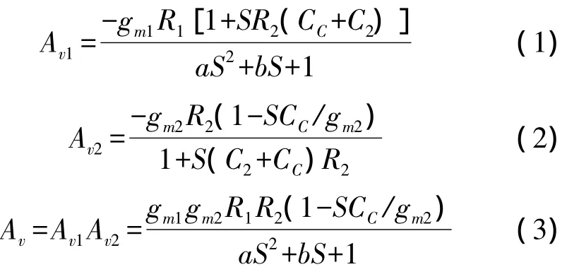
Where,a=R2R1C2C1+R1R2C1(CC+C1);b=R1C1+R1CC(1+gm2R2)+R2(C2+CC).
It is seen that the transfer functionAV1provides the poles forAVand produces a zero.AV2provides the zero forAVand produces a pole which will be eliminated by the zero in transfer functionAV1.Compensation capacitor acts as a parameter in denominator ofAV,which could be considered as a typical two-order multinomial.The discriminant of the multinomial changes the roots,which represent the poisons of poles as compensation capacitor varies.Therefore the difference between Miller theorem and simulation results could be understood easily.
2 MPC Amplifier
Further study of Miller effect shows that second stage will be just a compensation path,named Miller path,if output port is set at the first stage.It means the overalltransfer functionAVis equalto transfer functionAV1.
Based on Miller effect Miller Path,compensated(MPC)amplifier is present in Fig.3 and its small-signal circuit is also shown.M6,M7andCCact as compensation path.M8and M9behave as output stage to boost the gain of the amplifier.In small-signal circuitR1,C1andgm1are the first stage output resistance,output capacitor and transconductance respectively.R3,C3andgm3are the same parameters of the second stage.R2,C2andgm2are those of Miller compensation path.Cgd8represents the drain-gate parasitical capacitor.It is a very important parameter in design.It must be as small as possible compared withCCso that output stage will not influence compensation effect.IgnoreCgd8and derive the overall transfer function stage by stage,the new transfer functions are found as
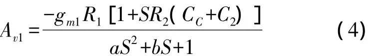
Where,a=R2R1C2C1+R1R2C1(CC+C1);b=R1C1+R1CC(1+gm2R2)+R2(C2+CC).

Fig.3
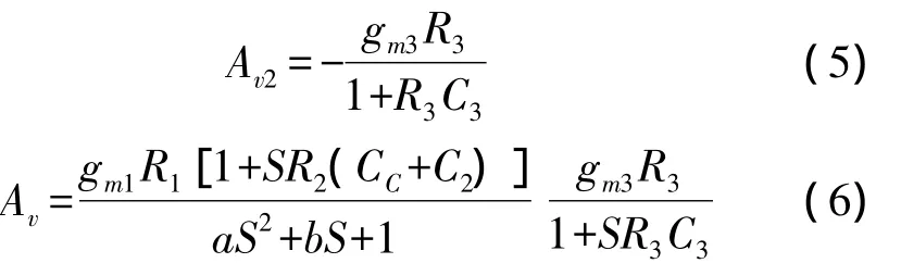
It is clear thatAVwill perform as two-order system if the compensation conditionR2(CC+C2)=R3C3is satisfied.BecauseC2could be very small,Miller theorem acts and the first stage pole,the dominant one,will be pushed to low frequency and the non-dominant pole will be at very high frequency.They could be found approximately as
There is no right-half-plant zero in the function.Therefore,nulling resistance[5]or other zero cancellation technique[2]could be avoided.As the representation of Eq.(8),UnityGainFrequency(UGF)willbe expanded.BecauseCL≥CC≥C2andR2,R3could be expressed as 1/(λIds),compensation condition could be simplified as:

CCis always at the level of 1 pF to save the chip area andCLmay be 100 pF such as the parasitical capacitor of power transistor in low drop-out voltage regulator.In that case the proportion ofI9andI7will be huge and not practical.So the pole and the zero could not be completely canceled.There must be a tradeoff between frequency compensation and power dissipation.
3 Simulation Results
Assume thatCLis 100 pF,CCis 2 pF,the prospective gain is 60 dB and UGF is 1 MHz.To achieve the goal,MPC amplifier is designed and simulated for 0.6 μm 30 V BCD process according to the parameters in Table 1.The proportion ofI9andI7is approximately set as 11:2 and power supply is 5 V.
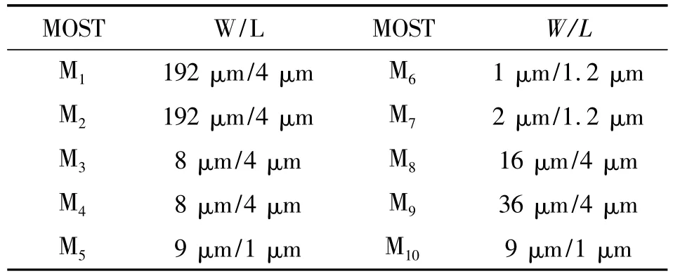
Table 1 Parameters of MOST in MPC amplifier(W/L)
It is shown in Fig.4 that MPC amplifier in this work has dc gain of 75 dB and UGF of 4.4 MHz when phase margin is 62.4°.Finally,large load capacitor is driven by two-stage amplifier using Miller path compensation.

Fig.4 Frequency response of MPC amplifier
The influence ofCCand the length of M7,L7,on compensation effect are also studied,because they both change the position of compensation zero under compensation condition.Table 2 and Table 3 show the results.It is seen in Table 2 that longer transistor M7expands UGF but reduces phase margin at unity gain frequency.Meanwhile,the worst phase margin and the frequency where it happens also change.It is the reason that longer M7makes its output resistance higher.According to Eq.(7),the dominant pole will be pushed to low frequency in that case.That will be helpful to expand the band width.Because the compensation is not built on complete cancellation of load-pole and compensation-zero,the effect of compensation will be carried to at higher frequency when output resistance becomes lower.And the phase margin will be worse at mid-frequency.It is shown in Table 3 that phase margin will get better asCCbecomes larger.Because load-pole and compensation-zero will move towards each other in that case,and the response of MPC amplifier performs likes a single-pole system.
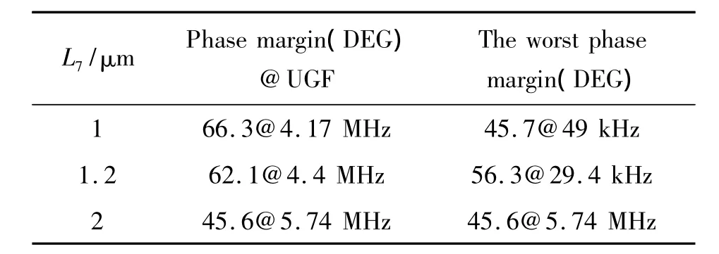
Table 2 The effect of W7in MPC amplifier

Table 3 The effect of CCin MPC amplifier
Simulations on transient response are done to verify the effect of Miller path compensation.Fig.5 shows the results of both large signal transient response and small signal one.It is seen that the set-ups of output voltage are achieved well and no ring or big overshoot happen.
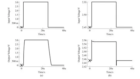
Fig.5
4 Conclusion
In this work MPC amplifier is designed and is discussed further based on the study of Miller effect.MPC amplifier could drive large load capacitor by a small compensation capacitor only 2 pF if the drain-gate parasitical capacitor is kept to low value.The effects of parameters in Miller path,such as compensation capacitor and length of M7,have also been discussed.This compensation method could also be used in any voltage amplifier where high impedance exists.
[1]Yang H C,Allstot D J.An Equivalent Circuit Model for Two-Stage Operational Amplifiers[C]//Circuits and Systems,1988,IEEE International Symposium,1988,1:635-638.
[2]Paul R Gray,Robert G Meyer.Analysis and Design of Analog Integrated Circuits[M].4 Ed.New York:John Wiley and Sons,2001.
[3]Filipkowski A.Poles and Zeros in Transistor Amplifiers Introduced by Miller Effec[C]//Education,IEEE Transactions on Volume 42,Issue 4,1999,349-351.
[4]Mazhari B.On the Estimation of Frequency Response in Amplifiers Using Miller’s Theorem[C]//Education,IEEE Transactions on Volume 48,Issue 3,2005,559-561.
[5]Yang H C,Allstot D J.Modified Modeling of Miller Compensation for Two-Stage Operational Amplifiers[C]//Circuits and Systems,1991,IEEE International Sympoisum vol.5 on 11-14,1991,2557-2560.
[6]Leung K N,Mok P K T.Three-Stage Large Capacitive Load Amplifier with Damping-Factor-Control Frequency Compensation[J].IEEE Journal of Solid-State Circuit,2000,35(2):221-230.
[7]Rincom-Mora G A.Active Capacitor Multiplier in Miller Compensated Circuits[J].IEEE J Solid State Circuits,2000,35(1):26-32.
[8]Eschauzier R G H,Kerklaan L P T,Huijsing J H.A 100 MHz 100 dB Operational Amplifier with Multipath Nested Miller Compensation Structrue[J].IEEE J Solid State Circuits,1992,27(12):1709-1717.
