Characterization of Fundamental Logics for the Sub-Threshold Digital Design
2013-11-26YanMingHeYaJuanHeYangMingLiShaoWeiZhenandPingLuo
Yan-Ming He, Ya-Juan He, Yang-Ming Li, Shao-Wei Zhen, and Ping Luo
1.Introduction
With the development of very large scale integrated circuites (VLSI) techniques, the integrity of system-on-chip(SoC) chips has drastically increased, which increases the power dissipation of electronic devices.The minimum energy consumption is desired for some applications to extend the battery life, such as the portable device,micro-sensor, and radio frequency identification devices(RFID)[1]-[4], for which recharging the battery is impossible or inconvenient.Sub-threshold voltage designs can be an effective way to realize ultra-low power systems.It enables circuits to operate at the sub-threshold voltage, achieving the minimum energy per operation[5].Previous research has proved the lowest usable supply voltage for the complementary metal-oxide-semiconductor (CMOS)transistor is under the threshold voltage of the CMOS transistor[6].
Modern electronic design automation (EDA) tools make it possible to integrate millions, even billions, of transistors on a single chip.But the implementation of a digital design is based on a standard cell library.Thus, a sub-threshold library is indispensable to enable the design flow for the sub-threshold designs.In this paper, a design methodology for the sub-threshold cell library is proposed,the structure and size of each cell is optimized based on the existing standard cell library.The characterization flow is illustrated in 0.13 μm CMOS technology with the supply voltage of 300 mV.
2.Digital Cell Library
The purpose of enabling the design to operate at a sub-threshold supply voltage is to achieve the minimum energy per operation.A minimum energy model is indispensable for the theoretical analysis of a design in the sub-threshold regime[7].Furthermore, an optimized digital cell library is also necessary to serve the design better and meet the design specifications.
2.1 Minimum Energy Model
From the previous research, it is known that the minimum energy point occurs at the sub-threshold regime[5].here the analysis on an energy model gives the exact equation of the optimum supply voltage.An inverter is taken as an example, the delay of an inverter is given as
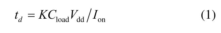
where Cloadis the output capacitance of the inverter, Vddis the supply voltage, K is the fitting parameter, and Ⅰonis the driving current of the inverter.For the sub-threshold voltage case, Ⅰonis expressed as
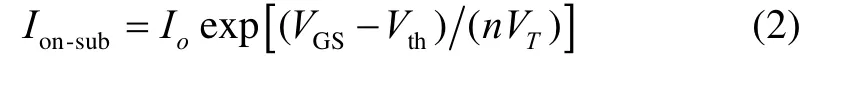
where Ⅰois the drain current when VGS=Vth, and Vthis the threshold voltage of the metal-oxide-semiconductor(MOS) transistor.AndWeffis the effective width of MOS transistor’s channel , L is the length of the MOS transistor’s channel, COXis the capacitance of gate oxide layer,nμ is the mobility of carriers, VTis the thermal voltage, n is a parameter determined by the technology[8].This equation ignores the drain induced barrier lowering (DIBL) effect on Ⅰon-sub.Combining (1) and (2) gives the delay equation of an inverter in the sub-threshold regime:

For a more generic case, the delay time of a design can be expressed as Td=LDtd, where LDis the logic depth of the design’s critical path, so the operational frequency of this design is f=1/Td.The power of a digital circuit consists of two parts: the dynamic power, Pdynamic, and leakage power,Pleakage, both of which are given as
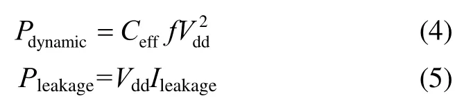
where Ceffis the effective switched capacitance of the design, including the active factor, f is the operational frequency and Vddis the supply voltage, and Ⅰleakageis the leakage current, which is mainly the sub-threshold current when VGS=0.So the energy for each operation is derived from (3), (4), and (5):
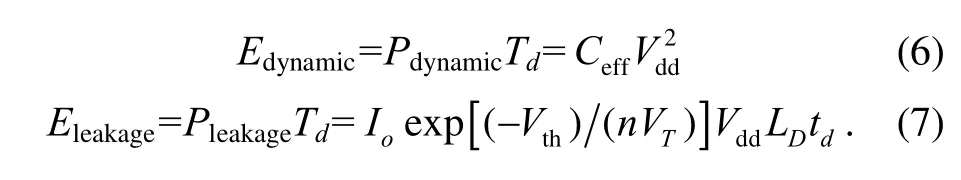
Total energy consumed by each operation is: Etotal=Edynamic+Eleakage.To find the minimum energy point, we calculate the derivative of Etotaltowards Vdd, and set the equation to zero:

Simplifing (8), we have:
The optimum supply voltage for the minimum energy point is derived by solving the above Lambert W function[9].
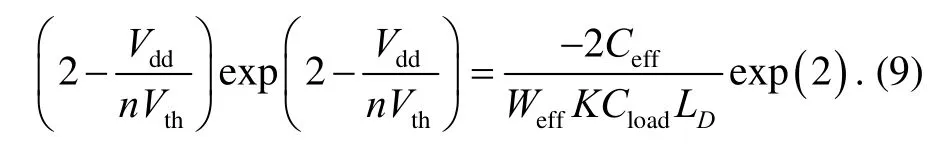
Generally speaking, the threshold voltage for a technology is fixed, so using (3), Td=LDtd, and f=1/Td, the relationship between Vthand Vddis given as
Since Vthis fixed for a particular design, the optimum Vddis derived from (9) to satisfy the sub-threshold condition: Vth>Vdd.There is a maximum frequency fmax, if the design’s operating frequency is larger than that, Vddwill be larger than Vth, the above model will not hold.
2.2 Cell Design Considerations for the Sub-Threshold Operation
The operation of conventional cells from the standard cell library in the sub-threshold regime is not exactly the same as that in the above-threshold regime.In this section,we first look into the operation of fundamental logic cells in the sub-threshold regime.Then, to ensure the functionality of these cells, some optimizations on the size and logic styles are introduced.Both combinational logics and sequential logics are involved.For combinational logics,the number of stacking and parallel transistors is constrained for obtaining a larger Ⅰdriving/Ⅰleakageratio.For sequential logics, the critical transistors in the cell are upsized to maintain the voltage of certain node at a correct level.
A.Design Example: A Sub-Threshold Ⅰnverter
The analysis of the minimum supply voltage is started with an inverter, and then extended to other standard cells in the library.The inverter is assumed with the minimum sized n-channel MOS (NMOS), and the width of p-channel MOS (PMOS) is sized to ensure a 10%Vddto 90%Vddoutput swing.First, a logic “0” is applied to the input node,the driving current from PMOS is supposed to charge the output node to logic “1”, which is called Ⅰdriving.The leakage current throw NMOS is called Ⅰleakage, and the ratioⅠdriving/Ⅰleakageindicates the functionality of a logic cell.In the sub-threshold regime, the driving current Ⅰdrivingfrom PMOS decreases exponentially with the supply voltage.So a largely reduced Ⅰdriving/Ⅰleakagemay cause that the output node fails to be pulled up to 90%Vdd.To solve this problem, the width of the PMOS, Wp, needs to be upsized, so the stronger Ⅰdrivingis able to pull the output voltage up to 90%Vdd.Especially in a strong NMOS/weak PMOS corner,the Wpneeds to be even larger.A minimum Wpwhich can drive the output voltage to 90%Vddis defined as Wpmin.
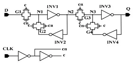
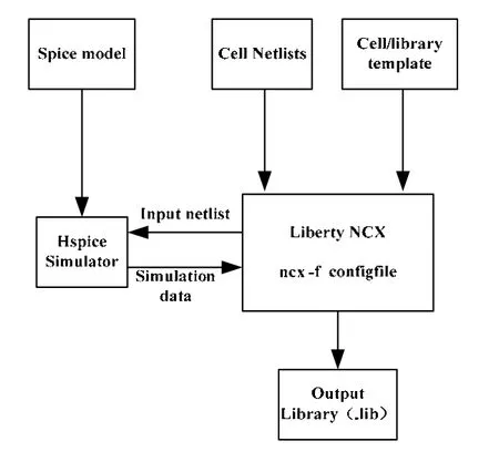
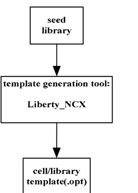
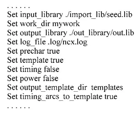
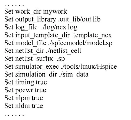
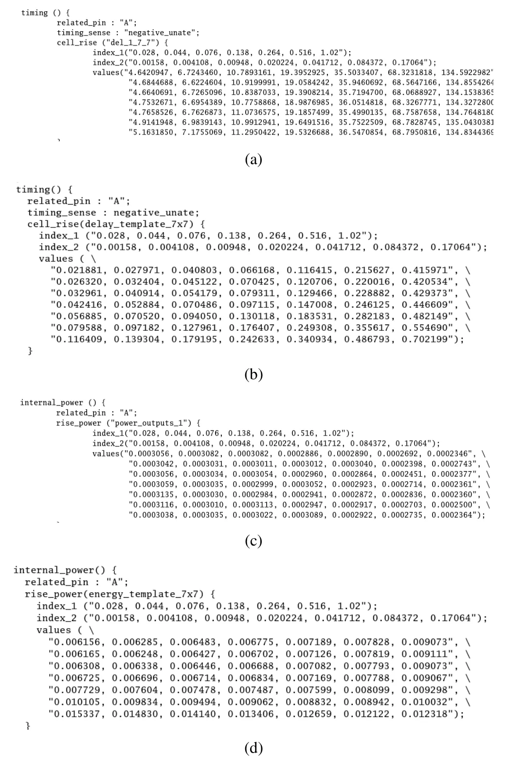
Further, a logic “1” is applied to the input, and the driving current from NMOS is supposed to pull the output voltage down to the logic “0”.But the leakage current from a large width PMOS will charge the output node, and the output node may fail to drop below 10%Vdd.So Wpcannot be upsized too much.Especially for a weak NMOS/strong PMOS corner, the Wpshould be even smaller, the largest Wpwhich allows the output voltage to be pulled below 10%Vddis defined as Wpmax.We simulate the Wpminand Wpmaxcorresponding to different voltages from 50 mV to 200 mV at a typical corner.In the simulation, Wnis in the minimum size, and Wp/Wnis changed from 1 to 80 in different voltages.By observing the output voltage of the inverter,Wpminfor 90%Vddand Wpmaxfor 10%Vddcan be achieved.The result is illustrated in Table 1.To ensure the output swing of 10%Vddto 90%Vdd, Wpshould satisfy the condition:Wpmin Table 1: Wpmin and Wpmax for typical corner Table 2: Wpmin and Wpmax for the worst case As the simulation result shows, if an inverter is supposed to operate at the sub-threshold voltage, its size needs to be set in a reasonable range. B.Combinational Logics The cells designed in a conventional library may have some problems at the sub-threshold regime.First, a cell with too many transistors in parallel may induce a large leakage current, which will reduce the Ⅰdriving/Ⅰleakageratio and cause the node of the cell fail to maintain a stable voltage.Second, a cell with large stacked transistors will cause the driving current to diminish.This will also reduce the Ⅰdriving/Ⅰleakageratio, and cause the output node of the cell fail to be charged to an ideal voltage.Designers should avoid using cells with large stacked devices and with too many devices in parallel.Since NMOS has a stronger driving current than PMOS, to avoid stacked PMOS, the NAND logic is preferred rather than the NOR logic[10],Third, the cells with transmission gates may induce the sneak leakage.To eliminate this flaw, buffers are added to the input and output of this kind of cells. C.Sequential Logics The D flip-flop is the most commonly used sequential cell in the digital design.The traditional type D flip-flop is illustrated in Fig.1, which is triggered by the positive edge of the clock signal.It may have some problems in sub-threshold regime[11].We consider two kinds of failures.First, when G1 is closed and G2 is opened, the feedback loop consisting of INV1, INV2, and G2 is supposed to maintain the voltage of nodes N1 and N2 at a stable level.But in the sub-threshold regime, the Ⅰdriving/Ⅰleakageratio is small and the large leakage current through INV2 may pull the voltage of N1 towards the wrong side and cause the voltage unstable.To solve this problem, the size of inverters in the feedback loop needs to be enlarged, so the strong driving current can maintain the voltages of N1 and N2 at a stable level. Second, when the clock signal is “0” and the D signal changes from “0” to “1”.The voltage of N2 changes from“1” to “0”.As G3 is closed, the output voltage at Q is not supposed to change.But when this D flip-flop operates at the sub-threshold regime, the leakage current of G3 may be large enough to change the voltage of N3, and cause the Q output to change before the active edge.The circuit fails to work synchronously with the clock signal.To avoid this kind of failure, the INV3 and INV4 need to be enlarged, so the driving current can be strong enough to overcome the leakage current through G3. Therefore, if the D flip-flop operates correctly in the sub-threshold regime, the size of transistors should be adjusted to avoid the potential failures. The purpose for characterization is to generate a technology library file (.lib file).It contains the logic,timing, and power information of each cell in the library.This file is necessary for synthesis, placement, routing process, and design verifications. The content in technology library can be classified into two parts: the head section and cell section[12].The head section contains the process information, delay model,operating condition, wire load model, unit of each parameter in the file, etc., which are the information used throughout the technology library.The other part is the cell section, which gives the information of each particular cell,such as the cell’s area, each pin’s direction, and the propagation delay from each input to output under different conditions. During the synthesis and placement&routing (P&R)process, the information in the technology library is used to elevate the cell’s function and performance, in order to choose the proper cells to meets the design constraints. In this design, we perform the characterization with the Synopsys Liberty NCX[13].The basic mechanism is illustrated in Fig.2: Liberty NCX reads in the netlist files,template files, and the Spice model file of the technology.Then the simulator, such as Hspice or Spectre, is invoked to perform the simulation for each cell.After that, Liberty NCX writes the data extracted from Hspice simulation results to a technology file. Fig.1.Schematic of a transmission gate D flip-flop. Fig.2.Characterization flow. Netlist: The netlist of each cell is extracted from their layouts, using the PEX function of the software Calibre.Each cell contains three files: cellname.pex.netlist.pex,cellname.pex.netlist.cellname.pxi, and cellname.pex.netlist;then the name of the file cellname.pex.netlist is changed into cellname.sp in order to be recognized by Hspice.The netlist describes the schematic and parasitic resistance&capacitance (RC) parameters of the cell.These files will be used by Hspice to generate the simulation data.Fig.3 shows the generation of the netlist[14]. Model file:The model file is the technique file which is necessary for Hspice to perform the simulation.Library described in this paper is based on 0.13 μm CMOS technology.The model file “ms013_io33_v2p5.lib” is offered by the foundry.It gives the parameters of each circuit element used in the cell’s netlist, including the MOS transistor, ploy resistor, metal-insulator-metal (MIM)capacitance, etc.The content of the model file is as follows:lib“/home/tdc_rezor/heyanming/libertyncx/spicemodel/ms 013_io33_v2p5.lib” tt. Liberty NCX uses the data from simulation results and writes them back to the output library file.The template file specifies the data to be used.There are two kinds of template files in the template directory: one library template for the whole library and the other template files for each cell in the library.They separately specified the parameters contained in the head section and cell description part of the library. Fig.3.Netlist generation. Fig.4.Templates generation flow. Fig.5.Templates generation. The template files can be written by hand according to the syntax[12].But this way is complicated and inefficient.A more efficient and convenient way is to generate templates from a seed technology library by Liberty NCX,which is shown in Fig.4.The seed library used in this paper is provided by the foundry whose nominal operating voltage is 1.2 V.The script that Liberty NCX uses for generating template files is illustrated in Fig.5. In Fig.5, several options are set for the generation of template: the input_library is the library used as a seed library; the output_library is the output library of characterization; the “prechar” is set to be true, which allows the Liberty NCX to write information from the seed library to the template files.The information in the template files can be modified according to users’requirements.Power and timing are set false to indicate that this script is just used to generating template files, not characterization.The “timing_arcs_to_template” is set true,which indicates that the “timing arcs”, which appears in the seed library, are written to templates[13]. After the templates are generated, simulation options in the template files should be modified, such as adjusting the operating voltage from 1.2 V to 300 mV, extending the simulation time, and modifying the indexes values.In this way, the templates are able to model the behavior of the cells in the sub-threshold regime. After all the input files are ready, Liberty NCX runs the script shown in Fig.6 and completes the characterization. Fig.6.Characterization control. Fig.7.Timing and power information in characterization results:(a) propagation delay for INV in sub-threshold library, (b)propagation delay for INV in the seed library, (c) internal power for INV in sub-threshold library, and (d) internal power for INV in the seed library. This script is used for the characterization of the sub-threshold library under the 300 mV supply voltage.The output_library specifies the name and directory of the output library file after characterization.The input_template_dir defines the directory storing the template files Netlist_dir/netlist_suffix that specifies the directory and suffix of each cell’s netlist.The simulator_exec specifies the simulator used to generate the simulation results, and the simulation_dir gives the directory storing the simulation results.The timing/power is set true, which tells Liberty NCX that this script is used for characterization, and Liberty NCX will write power and timing information from simulation results to the output library.The nlpm/nldm is also set true, which indicates Liberty NCX that the nonlinear delay/power model is used in the output library to store the power/timing information. The result of characterization is a technology library file whose cells operate in the sub-threshold regime, and the timing and power information in it is shown in Fig.7. Fig.7 (a) shows the propagation delay for the INV cell in the sub-threshold library.Compared with the same propagation delay in the 1.2 V seed library which is showed in Fig.7 (b), the propagation delay in the sub-threshold library is largely increased.This is because the INV cell operates in sub-threshold regime, and the driving current is much smaller.Fig.7 (c) shows the internal power of the INV cell in the sub-threshold library.Compared with that in the 1.2 V seed library shown in Fig.7 (d), the internal power in the sub-threshold library is largely decreased.This is because the supply voltage is decreased from 1.2 V to 300 mV. In this paper, a methodology to characterize a cell library in the sub-threshold regime is proposed based on 0.13 μm CMOS technology with the supply voltage of 300 mV.The results of the characterization show that the fundamental logics in the new library can operate properly in the sub-threshold regime.Their delay and power metrics in the technology library are coincident with the characteristics of the sub-threshold cells. [1]R.Weinstein, “RFID: a technical overview and its application to the enterprise,” ⅠT Professional, vol.7, no.3,pp.27-33, 2005. [2]L.Schwiebert, S.Gupta, and J.Weinmann, “Research challenges in wireless networks of biomedical sensors,” in Proc.of the 7th Annual Ⅰnt.Conf.on Mobile Computing and Networking, New York, 2001, pp.151-165. [3]A.Mainwaring, D.Culler, J.Polastre, R.Szewczyk, and J.Anderson, “Wireless sensor networks for habitat monitoring,” in Proc.of the ACM Ⅰnt.Workshop on Wireless Sensor Networks and Applications, New York, 2002, pp.88-97. [4]A.Cerpa, J.Elson, D.Estrin, L.Girod, M.Hamilton, and J.Zhao, “Habitat monitoring: application driver for wireless communications technology,” in Proc.of the ACM SⅠGCOMM Workshop on Data Communications in Latin America and the Caribbean, San Jose, 2001, pp.20-41. [5]A.Wang, B.H.Calhoun, and A.P.Chandrakasan,Sub-Threshold Design for Ultra Low-Power Systems, New York: Springer, 2006, pp.10-11. [6]R.M.Swanson and J.D.Meindl, “Ion-implanted complementary MOS transistors in low-voltage circuits,”ⅠEEE Journal of Solid-State Circuits, vol.7, no.2, pp.146-153, 1972. [7]B.H.Calhoun and A.Chandrakasan, “Characterizing and modeling minimum energy operation for sub-threshold circuits,” in Proc.of the 2004 Ⅰnt.Symposium on Low Power Electronics and Design, Newport Beach, 2004, pp.90-95. [8]X.-B.Chen, Q.-Z.Zhang, and Y.Chen, Microelectronics Decives, Beijing: Publishing House of Electronics Industry,2011, pp.216-217 (in Chinese). [9]R.M.Corless , G.H.Gonnet , D.E.G.Hare , D.J.Jeffrey,and D.E.Knuth, “On the Lambert W function,” Advances in Computational Mathematics, 1996, doi: 10.1.1.112.6117. [10]M.Liu, H.Chen, C.Jia, and Z.-H.Wang, “Design of a sub-threshold 32bit data path,” Journal of Tsinghua University (Science and Technology), vol.50, no.1, pp.9-12, 2010 (in Chinese). [11]W.Jin, S.Lu, W.-F.He, and Z.-G.Mao, “Robust design of sub-threshold flip-flop cells for wireless sensor network,” in Proc.of ⅠEEE/ⅠFⅠP the 19th Ⅰnt.Conf.on VLSⅠ and System-on-Chip, Hong Kong, 2011, pp.440-443. [12]Library Compiler User Guide, Volume 1, Synopsys, Inc.,Mountain View, 1998, pp.2-1-2-49. [13]Liberty NCX User Guide, Version F-2011.06, Synopsys,Inc., Mountain View, 2011. [14]Calibre xRC User’s Manual, Mentor Graphics Co.,Wilsonville, 2008.

3.Characterization
3.1 Technology Library
3.2 Data Preparation
3.3 Templates

3.4 Characterization
4.Results
5.Conclusions
杂志排行
Journal of Electronic Science and Technology的其它文章
- FPGA-Based Network Traffic Security: Design and Implementation Using C5.0 Decision Tree Classifier
- Saudi License Plate Recognition Algorithm Based on Support Vector Machine
- Mobile Web Middleware of NFC Context-Awareness Applications
- Metamaterial Absorbers in Terahertz Band
- Analysis of the Signal of Singing Using the Vibrato Parameter in the Context of Choir Singers
- Broadcasting with Controlled Redundancy and Improved Localization in Wireless Sensor Networks