Metamaterial Absorbers in Terahertz Band
2013-11-26QiYeWenHuaiWuZhangQingHuiYangandManManMo
Qi-Ye Wen, Huai-Wu Zhang, Qing-Hui Yang, and Man-Man Mo
1.Introduction
Metamaterials (MM) are artificially constructed electromagnetic (EM) materials which have the extraordinary physical properties that the natural materials do not have.They consequently have many applications,such as negative refractive index[1], superlenses[2],cloaking[3]and thermal emitters[4].A recent example for application of metamaterial is the creation of a resonant absorber at terahertz (THz) frequencies.The MM absorbers are generally composed of a MM layer and a metal plate layer separated by a dielectric spacer.With this kind of novel structure, unity absorptivity can be realized by matching the impedance of MM absorbers to free space.Such an absorber would be of particular importance at THz frequencies where it is difficult to find naturally occurring materials with strong absorption coefficients that are also compatible with standard microfabrication techniques.MM absorbers are very attractive in real applications due to its high absorption, low density, thin thickness, and integration flexibility[1]-[6].Besides that, wide-angle, polarization insensitive and even multi-bands/broadband absorption can be achieved through properly device designing[7]-[11].All these features make MM absorbers very useful in areas such as EM detector/imager, anti-electromagnetic interference, stealth technology, phase imaging,spectroscopy, and thermal emission.
In this paper, basic concepts and some recent progresses we made on THz MM absorbers are introduced and discussed.In Section 2 we give a simple introduction to the basic structure and the working principle of MM absorbers.A transmission line model was proposed to describe the devices and the asymmetry absorption phenomenon was explained.A dual-band MM absorber was designed and realized in Section 3, following by a demonstration of broadband THz absorbers realized in Section 4.The article closes with a final conclusion and outlook in Section 5.
2.Basic Structure and Working Principle of Metamaterial Absorbers
The first metamaterial based absorber was proposed by Landy et al.in the microwave band[1].It is called “a perfect metamaterials absorber” because nearly 100% absorption can be achieved theoretically.A single unit cell of the absorber consists of three layers as shown in Fig.1[1].The top layer is the electric split-ring resonator (eSRR), the middle layer is isolation layer (such as polyimide), and the bottom layer is rectangular metal strip.Due to the lithography alignment and multi-step lithography process,the preparation process of the first MM absorber is complex.Experimentally, the maximum absorptivity only reaches to 70% at 1.3 THz due to the fabrication tolerance.An improved MM absorber was proposed by H.Tao et al., with the bottom metal strips replaced by a continuous metal film[2].This improved absorber operates quite well for both TE and TM radiation over a large range of incident angles(0-50°), and the measured absorbance was further improved to 97%.Therefore, the MM absorber with a continuous metal ground plane becomes the most commonly structure in the researches.
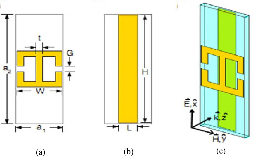
Fig.1.Basic structure of three layers metamaterial absorber: (a)the layer of metamaterial (eSRR), (b) the bottom metallic layer and (c) the unit structure include the dielectric layer.Figure adapted from Landy et al.[1].
The absorption mechanism of the MM absorber is as follows.First, by changing the geometry of the SRR and the thickness of the spacer, the impedance Z(ω) of the absorber can be designed to match the impedance of free space at a specific frequency (center frequency) resulting in zero reflection.Second, electromagnetic waves can not pass through the metallic ground plane, giving rise to zero transmission too.Thus, electromagnetic waves will be completely restricted in the device and finally be consumed.In principal, the MM absorber can absorb 100% of the narrow-band electromagnetic waves.It can be used in microwave, THz, and even light wave bands by adjusting the feature size of the unit cell.
Though more and more attention has been paid to the MM absorber, the mechanism of the near-unity absorption is still under studying.It is not clear that why the absorption is extensively enhanced after the MM structure and the wires structure being integrated into an absorber, and it is also unknown why the absorptions of MA is highly sensitive to the thickness of separated layer.More importantly, metamaterials can be usually treated as effective media.However, the effective medium theory has some problems in describing MA because the three-layer structured device does not exactly satisfy the homogeneous-effective limit, according to Caloz[12].A typical case is that the strong asymmetric absorption phenomenon cannot be fully explained by the effective medium model[13].The simulation results show dramatically different behaviors when the electromagnetic waves incident from the two opposite directions.For example, when light is incident from the front to the resonators the device acts as a perfect absorber, while when light is incident from the back to the ground plane the device behaves like a perfect mirror.Furthermore, the MA consists of only two metallic layers, thus are strongly inhomogeneous in the wave propagating direction, which is obvious in contrast to the effective medium model.
Here we introduce a transmission line (TL) mode to analyze the mechanism of the MM absorber[14].In the TL model as shown in Fig.2, it is assumed that the transverse electromagnetic (TEM) wave propagates through free space and the substrate with intrinsic impedances Ziand Zo,respectively.There are two assumptions for constructing the TL model.One is that coupling capacitor or coupling inductor between the eSRR layer and wires layer should be ignorable, so that these two layers can be individually modeled, as demonstrated in Fig.1.Another is that the THz wave normally incidents on the absorber plane with the electrical field parallel to the split gap of the eSRR.The TL model of eSRR proposed by Azad[15]is used to describe the eSRR layer, in which the LC resonance and dipole resonance each is represented by one group of L, C, and R,respectively, and the coupling between these two resonances is specified by the parameter M.The wires layer part is mimicked by the TL model developed by Fu et al.[16],with the only resonance expressed by one group of L, C,and R.The function of isolation layer is modeled by a transmission line which contains all EM related properties of the isolation layer such as ε, μ, and thickness.It connects the eSRR part and wire part.All the parameters are needed to be optimized until the S-parameters calculated by the TL model fit the simulation results.
Once all of the parameters in Fig.1 are determined, the S-parameters of the MA can be derived as follows.
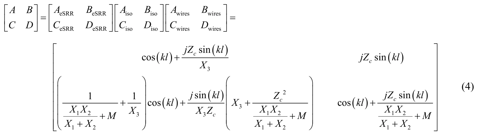
The ABCD matrix of eSRR structure layer, isolation layer (iso) and wires structure (wires) are

Fig.2.Transmission line model of metamaterial absorber.
and k is the wave vector of the TEM wave, l and Zcare the thickness and characteristic impedance of the isolation layer,respectively.
So the ABCD matrix of the MA is
Then the S matrix thus can be calculated as
In the TL model of the absorber, the R1, R2, and R3represent the components for energy consumption.The energy consumed by R1, R2, R3in two exciting conditions were calculated by our TL model, as shown in Fig.3.When the EM wave is emitted from eSRR to wires structure (the positive case), nearly 90% of the incident energy is consumed by R1, and about 10% consumed by R3.These results mean that the LC resonance of eSRR is predominant in the energy absorption to the EM wave, while the contribution from dipole resonance is very small and ignorable.In the negative case (from wires structure to eSRR), the total energy consumption of the absorber is very small.It is the wire structure which provides about only 6%energy loss to the incidence wave, and R1and R2contribute very little.These results unambiguously demonstrate and explain the asymmetric phenomenon of THz absorption.It also confirm that, for the absorber discussed here, it is mainly the LC resonance of the eSRR structure contributes to the strong absorption when EM wave propagate along the positive direction.
Abovementioned results give an insight into the basic function of each components of MM absorbers: 1) As hints by the TL model, the LC resonance of eSRR strongly affects the absorption characteristics of the absorber.It is also known that for eSRR, the inductance L is provided by its metallic loops and the capacitance C is induced by the splits of the ring[12].Thus the absorption curve of the absorber mainly depends on the framework of the eSRR.Of course, the effects of other components such as interlayer coupling and other resonance from Liand Ci(i=2, 3) are also not negligible.2) More importantly, the function of the isolation layer is to adjust the impedance of the metamaterials and enable the EM wave to enter into the device as much as possible.Therefore, the absorption is highly sensitive to the properties of the isolation layer, such as its thickness, permeability and permittivity.3) The role of wires structure is to enhance the reflection of EM wave thus benefits the trapping and absorbing of wave in the space between the two metallic layers.All these features revealed by TL model set the basic principles for the design of THz MM absorbers.
By this TL model, the asymmetric phenomenon of THz absorption is unambiguously demonstrated and explained.The strong absorption is found to be mainly related to the LC resonance of the eSRR structure.The isolation layer in the absorber, however, is actually an impedance transformer and plays key role in producing the perfect absorption.The studies by the TL model also show that the electromagnetic wave is concentrated on some specific location in the absorber.It indicates that the trapped electromagnetic wave in the absorber can be converted into thermal energy,electric energy or any kinds of other energy depending on the functions of the spacer materials.This feature as electromagnetic wave trapper has many potential applications such as radiation detecting bolometers and thermal emitter.
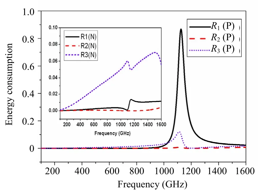
Fig.3.Spectrum of energy consumption of Ri (i=1, 2, 3) in TL model for the positive (P) and negative (N) incidence of the THz wave.
3.Dual-Band THz MM Absorbers
Most of the existed designs for perfect THz absorbers only have single-band response.Actually, design and fabrication of multi-absorptive metamaterials are potentially useful and attractive[9].It is also a possible step towards broadband THz absorber for microbolometers.Since our TL model suggest that the strong absorption is found to be mainly related to the LC resonance of the eSRR structure, an eSRR with dual band LC resonance are possible to construct a dual band absorber.
The designed single unit of the absorber consists of two metallic elements: an electric-field-coupled split resonance ring structure (eSRR), and a metal plate bottom layer.The eSRR unit cell is composed of two symmetrical single-resonant metamaterials with one invaginated in another, as shown in Fig.4 (a).The two single-resonant parts have different split gaps and different inductive loops,which will induce two different LC resonances.In order to maximize the absorption of the device, both the transmission and reflection should be minimized.The resonance of the eSRR would be tuned to approximately match the impedance z(w) to free space in order to minimize the reflectance at specific frequencies.At the same time, there is no transmission through the absorber across the entire frequency range under studied due to the shielding of the bottom metal plate.The total structure is constructed on a 500 μm SI-GaAs substrate as shown in Fig.4 (b).The complex dielectric constants ε of GaAs and polymide are 12.9+0.077i and 2.5+0.2i, respectively[3].Both the metal plate and the eSRR are made of Gold with conductance of 4.09×10⁷S/m.Utilizing the CST Microwave Studio, the structure of the absorber was optimized (simulating radiation at normal incidence with the electric field perpendicular to the split gaps) with the size parameters are listed in the caption of Fig.4 (a).The device was fabricated by sputtering of Ti(40 nm)/Au(800 nm) followed by spin coating with 10 μm polyimide.Another 200 nm Au film was sputtering deposited on the top of the polyimide film, and which was then patterned into the designed eSRR shape by reactive ion etching.The photograph of a unit cell and a portion of the fabricated absorber are shown in Fig.4 (c) and (d).The dimension of the fabricated eSRR structure is very close to the theoretically optimized value, and the size parameters are measured and listed in the caption of Fig.4 (c).
The reflection of the absorber was measured by a THz-TDS system with an incident direction of 30 degree off the normal direction.The measured reflection as a function of frequency is displayed in Fig.5.Two reflectivity minimums around 0.45 THz and 0.92 THz are clearly observed, confirming that the dual-band absorption is realized in our as-fabricated MA.Both reflective peaks are strong with the low-frequency minimum of 0.192 and the high-frequency minimum approaching 0.366, giving rise to strong absorption of 80.8% and 63.4%, respectively.The slight red-shift of the absorption frequency from the simulation is reasonably ascribed to the broadening of metal wires or split gaps of the eSRR structure, as indicated in Fig.4.

Fig.4.Dual-band terahertz metamaterial absorbers.(a) designed electric split ring resonator with a=60, b=120, d=4, h=55, l=28.6,t1=6, t2=4, t3=14, and t4=13, (b) perspective view of the designed absorbers, (c) a unit cell of the experimentally realized absorbers with eSRR size of a=61.8, b=119.6, d=4.4, h=54.6, l=28.2, t1=6.4,t2=4.2, t3=15.4, and t4≈13, all number denotes the size in unit of micrometers, and (d) photograph of a portion of the fabricated absorber.The period for the absorber unit is 140 μm×124 μm.
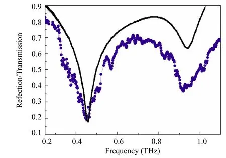
Fig.5.Measured reflection curve of the absorber (line+symbol)and the simulated transmission curve of the eSRR (smooth line).
4.Broadband THz MM Absorbers
The development of dual-band THz MM absorber paves the way to a broadband THz absorber since the absorption band can be expanded by merging several closely positioned resonant peaks in the absorption spectrum.In this section, we experimentally demonstrated a THz broadband absorber using a SiO2dielectric spacer.SiO2has excellent thermal, mechanical, and dielectric properties[17].Based on an SiO2layer, a narrow-band THz absorber has been previously studied[18].But a SiO2based broadband THz absorber has never been reported.As to the broadband MM absorber derived from combining multiple absorption peaks, the thickness of the dielectric layer is essentially important to the bandwidth.It is well know that the fabrication of SiO2films is a typical CMOS process.The film thickness can be precisely controlled and the large-area uniformity can also be warranted.All these features make SiO2very suitable for a broadband THz MM absorber.
The MM absorber is a three-layered device with the structure depicted in Fig.6.A Pt ground layer was separated from the top Al squares by a SiO2spacer.Specially, a structural unit of the absorber is composed of two mixed-size squares, as schematically illustrated in Fig.6 (c).The refractive index of SiO2is 2.0+0.025i at THz frequencies[19],[20].The conductivity of the Al and Pt is 1×10⁷S/m and 9.43×10⁶S/m, respectively.The periodic boundary conditions are set along the x and y axes directions, as indicated in Fig.6 (a).A plane wave vertically impacts on the front face of the structure, and as the excitation source, the electric field is polarized parallels to the x direction.Utilizing the CST Microwave Studio, the structure of the broadband absorber was optimized(simulating radiation at normal incidence) and the obtained size parameters were listed in the caption of Fig.6 (b)and (c).
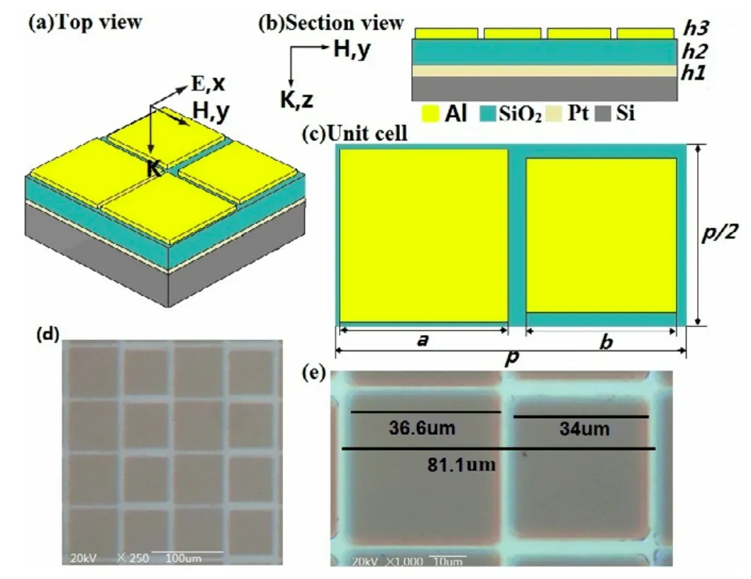
Fig.6.Schematic diagram of the broadband THz metamaterial absorber: (a) top viewm, (b) the section view of a portion of the designed absorber with h1=100 nm, h2=2 μm, h3=100 nm, (c) a simulated unit cell of the mixed-size square resonators with a=36.9 μm, b=34.2 μm, p=80 μm, (d) micrograph of a portion of the fabricated absorber, and (e) a cell structure of the fabricated absorber with a=36.6 μm, b=34 μm and p=81.1 μm.
Such a three-layered integrated structure was fabricated using microfabrication techniques.Firstly, a 200-nm-thick Pt/Ti film was E-beam evaporated on Si to form the bottom layer.The SiO2dielectric spacer with a thickness of 2 μm was deposited on Pt using plasma enhanced chemical vapor deposition (PECVD).Then a 200-nm-thick Al film was deposited on top of the SiO2film by e-beam deposition.Ultimately, mixed-size Al square arrays were patterned by wet etching with the size parameters defined in Fig.6 (a).A micrograph of a unit cell and a portion of the fabricated absorber are shown in Fig.6 (d) and (e).The size parameters are measured and listed in the caption of Fig.6(e).However, there are still some deviations due to the fabrication tolerances.For example, both squares are slightly smaller while the period is a little larger as compared to the designed structure.
The absorption characteristic of the sample was tested using a Fourier transform infrared spectrometer (FTIR) in a reflection geometry.The reflection coefficient measurement was taken with THz beam in reflection mode at 30°incidence angle from the normal direction, using a blank Pt coated substrate as the reference.A detailed description of this system can be found in [21].The total sample area for measurement was 1.5×1.5 cm2to prevent beam clipping.Measurements were conducted in a dry-air environment to mitigate the effects of water vapor absorption.The absorptivity was calculated byThe measured absorption as a function of the frequency is displa yed in Fig.7.Two absorption maximums around 2.58THzand2.65THz are clearly observed with absorption of 99.8% and 98.7%, respectively,between which the minimum absorptivity in the dip is still high to 91.8%.The width of the absorption top is 210 GHz if a strict criterion of 90% of the maximum absorption is defined, confirming that broadband absorption was realized in our fabricated absorber.
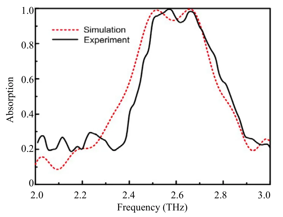
Fig.7.Measured (solid curve) and simulated (dash curve)absorption spectra curves of the MM absorber.
5.Future Development Trends of Metamaterial Absorbers
It is a few years time since the metamaterial absorber was first proposed until now, but the research has made great progress.The future development of metamaterial absorbers will move along the following direction.
Broadband absorber: narrowband absorber has important applications in the THz detection, but for absorbing, invisible, thermal emission and energy conversion, broadband absorbers have more useful values.Currently, the coverage of broadband absorbers based metamaterials is still relatively less, so the research of the broadband metamaterial absorbers will become a hot issue in the future.
Frequency tunable absorber: the frequency tunable absorber can absorb different frequencies of electromagnetic waves flexibility to achieve broadband absorption.In addition, the frequency tunable absorber can control the absorption level of specific frequency flexibility,and plays a similar role as a switch or invisible window.The frequency tunable absorber will be the important development trend of metamaterial absorbers in the future.
Absorber combined with functional materials: absorbers combined with functional materials will be another development trend of metamaterial absorbers, so a variety of different functions can be achieved.After electromagnetic wave is absorbed, it is usually transformed into heat in the middle dielectric layer.If the middle dielectric layer is replaced by other functional materials, it is possible to achieve a number of special performances.For example, the use of thermoelectric materials can transform the electromagnetic waves into electric energy in the specific area, which is an important application in the detection of electromagnetic waves.In addition, it will display many new features to combine with nonlinear materials, optical materials, piezoelectric materials, and phase change materials, etc.
[1]N.I.Landy, S.Sajuyigbe, J.J.Mock, D.R.Smith, and W.J.Padilla, “Perfect metamaterial absorber,” Phys.Rev.Lett.,2008, doi: 10.1103/PhysRevLett.100.207402.
[2]H.Tao, C.M.Bingham, A.C.Strikwerda, D.Pilon, D.Shrekenhamer, N.I.Landy, K.Fan, X.Zhang, W.J.Padilla,and R.D.Averitt, “Highly flexible wide angle of incidence terahertz metamaterial absorber: design, fabrication, and characterization,” Phys.Rev.B, 2008, doi:10.1103/PhysRevB.78.241103.
[3]H.Tao, N.I.Landy, C.M.Bingham, X.Zhang, R.D.Averitt,and W.J.Padilla, “A metamaterial absorber for the terahertz regime: Design, fabrication and characterization,” Opt.Express, 2008, doi: 10.1364/OE.16.007181.
[4]Y.Avitzour, Y.A.Urzhumov, and G.Shvets, “Wide-angle infrared absorber based on a negative-index plasmonic metamaterial,” Phys.Rev.B, 2009, doi:10.1103/PhysRevB.79.045131.
[5]N.I.Landy, C.-M.Bingham, T.Tyler, N.Jokerst, D.R.Smith, and W.J.Padilla, “Design, theory, and measurement of a polarization-insensitive absorber for terahertz imaging,”Phys.Rev.B, 2009, doi: 10.1103/PhysRevB.79.125104.
[6]R.Huang, Z.-W.Li, L.B.Kong, L.Liu, and S.Matitsine,“Analysis and design of an ultra-thin metamaterial absorber,”Progress in Electromagnetic Research B, 2009, doi:10.2528/PIERB09040902.
[7]B.Wang, T.Koschny, and C.M.Soukoulis, “Wide-angle and polarization-independent chiral metamaterial absorber,”Phys.Rev.B, 2009, doi: 10.1103/PhysRevB.80.033108.
[8]Y.-Q.Ye, Y.Jin, and S.-L.He, “Omnidirectional,polarization-insensitive and broadband thin absorber in the terahertz regime,” J.Opt.Soc.Am.B, vol.27, no.3, pp.498-504, 2010.
[9]Q.-Y.Wen, H.-W.Zhang, Y.-S.Xie, Q.-H.Yang, and Y.-L.Liu, “Dual band terahertz metamaterial absorber: design,fabrication, and characterization,” Appl.Phys.Lett., vol.95,no.24, pp.241111-241111-3, 2009.
[10]H.Tao, C.M.Bingham, D.Pilon, K.Fan, A.C.Strikwerda,D.Shrekenhamer, W.J.Padilla, X.Zhang, and R.D.Averitt,“A dual band terahertz metamaterial absorber,” J.Phys.D:Appl.Phys., 2010, doi:10.1088/0022-3727/43/22/225102.
[11]X.-P.Shen, T.-J.Cui, J.-M.Zhao, H.-F.Ma, W.-X.Jiang,and H.Li, “Polarization-independent wide-angle triple-band metamaterial absorber,” Opt.Express, vol.19, no.10, pp.9401-9407, 2011.
[12]A.C.Caloz and T.Itoh, Electromagnetic Metamaterial:Transmission Line Theory and Microwave Applications, New York: John wiley & Sons, 2005.
[13]Y.-X.Li, Y.-S.Xie, H.-W.Zhang, Y.-L.Liu, Q.-Y.Wen, and W.-W.Lin, “The strong non-reciprocity of metamaterial absorber: characteristic, interpretation and modelling,” J.Phys.D: Appl.Phys., 2009, doi:10.1088/0022-3727/42/9/095408.
[14]Q.-Y.Wen, Y.-S.Xie, H.-W.Zhang, Q.-H.Yang, Y.-X.Li,and Y.-L.Liu, “Transmission line model and fields analysis of metamaterial absorber in the terahertz band,” Opt.Express,vol.17, no.22, pp.20256-20265, 2009.
[15]A.K.Azad, A.J.Taylor, E.Smirnova, and J.F.O'Hara,“Characterization and analysis of terahertz metamaterials based on rectangular split-ring resonators,” Appl.Phys.Lett.,vol.92, no.1, pp.011119-011119-3, 2008.
[16]L.Fu, H.Schweizer, H.Guo, N.Liu, and H.Giessen,“ Synthesis of transmission line models for metamaterial slabs at optical frequencies,” Phys.Rev.B, 2008, doi:10.1103/PhysRevB.78.115110.
[17]D.Grbovic, N.V.Lavrik, S.Rajic, and P.G.Datskos,“Arrays of SiO2substrate-free micromechanical uncooled infrared and terahertz detectors,” J.Appl.Phys., vol.104, no.5, pp.054508-054508-7, 2008.
[18]F.Alves, B.Kearney, D.Grbovic, N.V.Lavrik, and G.Karunasiri, “Strong terahertz absorption using SiO2/Al based metamaterial structures,” Appl.Phys.Lett., vol.100, no.11,pp.111104-111104-3, 2012.
[19]M.K.Gunde and M.Macek, “Infrared optical constants and dielectric response functions of silicon nitride and oxynitride films,” Phys.Status Solidi A, vol.183, no.2, pp.439-449,2001.
[20]D.Y.Smith, E.Shiles, and M.Inokuti, “The optical properties of metallic aluminum,” in Handbook of Optical Constants of Solids, E.D.Palik, Ed.San Diego: Academic Press, 1998.
[21]C.Bolakis, D.Grbovic, N.V.Lavrik, and G.Karunasiri,“Design and characterization of terahertz-absorbing nano-Iaminates of dielectric and metal thin films,” Opt.Express, vol.18, no.14, pp.14488-14495, 2010.
杂志排行
Journal of Electronic Science and Technology的其它文章
- FPGA-Based Network Traffic Security: Design and Implementation Using C5.0 Decision Tree Classifier
- Characterization of Fundamental Logics for the Sub-Threshold Digital Design
- Saudi License Plate Recognition Algorithm Based on Support Vector Machine
- Mobile Web Middleware of NFC Context-Awareness Applications
- Analysis of the Signal of Singing Using the Vibrato Parameter in the Context of Choir Singers
- Broadcasting with Controlled Redundancy and Improved Localization in Wireless Sensor Networks