300 mm硅片精密化学机械抛光机几何参数优化
2012-08-08党宇星徐继平叶松芳肖清华闫志瑞张果虎周旗钢郭强生王东辉
党宇星 ,徐继平 ,刘 斌 ,叶松芳 ,肖清华 ,闫志瑞 ,石 瑛 ,张果虎,周旗钢,2,柳 滨,郭强生,王东辉
(1.有研半导体材料股份有限公司,北京 100088;2.有色金属研究总院,北京 100088;3.中国电子科技集团第四十五研究所,北京 100176)
1 Introduction
For more than half a century,prime silicon wafer is being used as the fundamental material for ULSI manufacturing[1~3].With the technology node of ULSI decreases to less than 20 nm and the diameter of the wafers increases to more than 300 mm,extremely tight requirements are being placed on both the shape of the prime wafer and the flatness of its surface.To fulfill thestringentrequirements in lithography device processing step during the 300 mm and below 90 nm ULSI manufacturing,the key geometry parameters are site front least square range(SFQR)and global backside ideal range(GBIR)[4].
Since the demonstration of chemical mechanical polishing(CMP)in the 1960s,it has been employed as the best technique for silicon wafer thinning and planarization[5].The final-touch CMP process can be divided into one-step,two-step,and three-step types.Generally,with moresteps thepolishing could achieve higher precision.Currently,three-step polishing,which includes:rough-polishing,intermediate-polishing and final-touch CMP,is the most acceptable polishing method.The main purpose of final-touch CMP is to achieve a clean and micro-roughness-free (haze-free)surface.At the same time,to keep the variation of the wafer geometry as trivial as possible or even an improvement during final-touch CMP is also necessary[6].
Recently,the first China-made 300 mm silicon wafer final-touch CMP machine was successfully made.During the qualification check,we have performed a series of experiments to ensure the quality of wafer surface could fulfill the specifications of ULSItechnology.Hereafter,we demonstrate a method to conserve or enhance the wafer thickness geometry with our machine.We perform experimentsby optimizing theprocessand adjusting own-designed polishing head accordingly.The effect on GBIRand SFQRvalues is analyzed with clearly different incoming geometries using a variety of polishing recipes.
2 Process
The acceptance check flow of prime wafer processing by final-touch CMP machine is shown in Fig.1.As we can see from Fig.1,the process flow of acceptance check of prime wafer processing can be summarized as follows:Firstly,the incoming 300 mm wafer finishing up grinding and edge-polishing was measured topography of the wafer with an advanced flatness/wafer characterization system ADE AFS-3220.Secondly,the surface of the wafer was double-side polished by CMP machine SPEEDFAM 20B.Thirdly,the wafer was pre-cleaned via the AKrion V3 Semi-Auto Bench with chemicals.Fourthly,which is the acceptance check step,the wafer was final-touch CMP with our own made final polishing machine PG-1201.During the polishing,the environmental temperature is constant at 20 and the humidity keeps at 46%.As we all know,it is important to maintain the environmental conditions for regular processing.There are two steps during the final-touch polishing.The first step is a rough polishing step which uses Suba 600 made by Rodel Inc.as polishing pad and SR310 made by Dupont Inc.as slurry.The second step is a finishing polish step utilizing 7355 polishing pad and Fujimi Inc.'s FGL-3900 as slurry.Before starting each polishing cycle,the polishing pad was conditioned in order to prevent the glazing effect.To verify if the topography conforms to our acceptance check standard,we measured the surface topography of the wafers with the advanced flatness/wafer characterization system ADE AFS-3220.
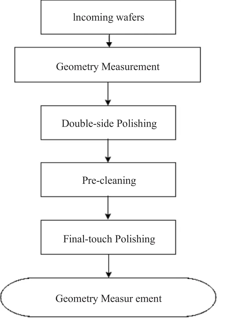
Fig.1 Process flow of the acceptance inspection process
3 Results and Discussion
The acceptance check process lasts about two months.Table 1 and Table 2 show the values and units of major parameters of platen 1 and platen 2 we first used,respectively.The major parameters include:polishing time(T),carrier down force(DF),retaining ring force(RF),and rotation speed of platen(SP).During the experiments,we used four steps recipe.After releasing the vacuum pressure,the first step was to gradually push down the wafer on the platen with backing pressure from the carrier.The second step was the first actual polishing step with the carrier down force increases.The third step was the vital step for removing the damaged layer induced by double-side polishing.The fourth step aimed to have a super smooth surface.

Table 1 Parameters for the polishing platen 1

Table 2 Parameters for the polishing platen 2
According to IC manufacturer's requirement,two differentthickness geometry properties of polishing wafers are of the major interest.After the negotiation with our customer,the acceptance criterion for the geometry property of the wafer surface for 90 nm technology node is determined as:
1)Variation of(G)lobal(B)ackside(I)deal Focal Plane(R)ange(GBIR):

If GBIRvar<0,it shows that the global flatness of the wafer surface after CMP is better than that of the wafer surface before CMP.If GBIRvar>0,it shows that the global flatness of the wafer surface after CMP is worse than before CMP.However,regardless how GBIRchanges,as long as the variation satisfies the condition that:

the GBIRafter CMP satisfies our requirement.
2)Variation of(S)ite (F)rontside Least S(Q)uares Focal Plane(R)ange(SFQR)
We define:

Thereby:

If SFQRvar<0,it demonstrates that the maximum site flatness of the wafer surface after CMP is smaller than that of the wafer surface before CMP.If SFQRvar>0,it demonstrates that the maximum site flatness of the wafer surface after CMP is larger than before CMP.
The acceptance check criterion of SFQRvariation for 90 nm technology node is determined as:with a site size of 25 cm×25 cm including partial size:

We arranged experimental wafers as 10 pieces for each group and perform experiments according to the process flow in Fig.1.Hereafter in paragraphs and figures,we use"GBIRbef"to indicate GBIRvalue before polishing,"GBIRbef"to indicate GBIRvalue after polishing,and"GBIRvar"to represent GBIRvariation.The similar definition applies to those values of SFQR.The left primary axis is for GFQRvalue and the right secondary axis is for SFQRvalue.The acceptance criteria are indicated by the horizontal lines in figures.
After the measurement of Lot 1,we have the results as shown in Fig.2.As sketched here,all SFQRvarof the ten pieces are smaller than 0.2 μm while SFQRvarof the last wafer is larger than 0.05 μm,which does not conform to the specification.Therefore,there are nine out of ten pieces of wafers qualified the test while one piece failed.
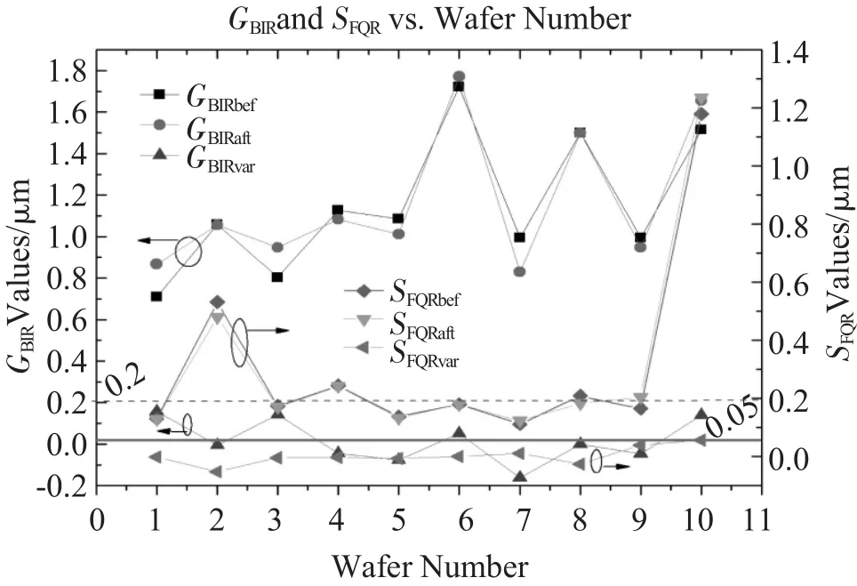
Fig.2 Geometry parameters of Lot 1
As to Lot 2,we have the result shown in Fig.3.As illustrated,SFQR var of the last wafer does not meet our requirement.Hence,for this lot,there are nine out of ten wafers passed the acceptance check.

Fig.3.Geometry parameters of Lot 2
For Lot 3,the measured results are shown in Fig.4,where we can observe that wafers No.1,4,6 are not accepted.Hence,there are seven out of ten wafers passed the acceptance check.The ratio of acceptance is about 70%.
For Lot 4 to Lot 10,the measured results are shown in Fig.5.As we can see from the figure,for the 70 pieces examined,there are altogether 57 pieces of wafer passed the acceptance criteria.The ratio of acceptance reaches 81%.
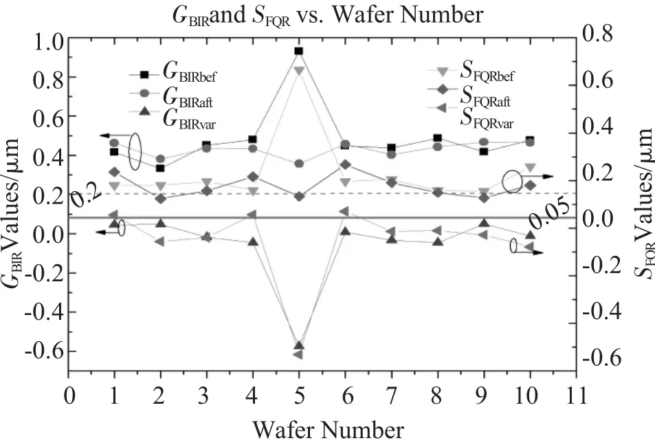
Fig.4 Geometry parameters of Lot 3
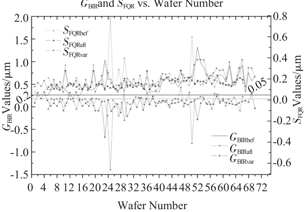
Fig.5 Geometry parameters of Lot 4 to Lot 10
However,with the time,the performance of CMP deteriorates.In Fig.6,the results of Lot 11 to Lot 15 are shown.Only 20 out of 50 pieces were accepted,which manifested that some problems existed with the present polishing process.It is worth while examining the wafers more closely.
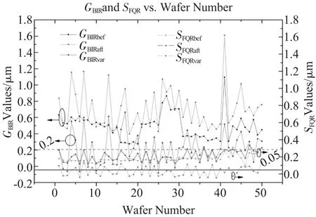
Fig.6 Geometry parameters of Lot 11 to Lot 15
Let us now attempt to extend the observation into the consideration of the polishing head structure.The structure of the polishing head is revealed in Fig.7,in which the innermost two pressure rings are for backing pressure 1;the intermediate two rings are for vacuum pressure during operation;the outmost two rings are for backing pressure 2.During CMP,we set the backing pressure 1 and 2 at the same value.This brings us to the consideration of the geometries of wafers.
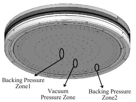
Fig.7 The structure of the carrier head
Therefore,we measured the topography of rejected wafers,which are schematized in Fig.8.As the diagram indicates,the contour of the wafer before polishing is clear concave thickness profiles.The variation of GBIR is 0.221 μm which is larger than our required 0.2 μm.It demonstrates deteriorates of the geometry.In order to achieve good geometry parameters GBIR and SFQR,we have to achieve a contour as flat as possible,or at least it should be as close to the shape before polishing.In other words,an edge-fast removal would have been necessary.However,under the same baking pressure values for zone 1 and zone 2,it is hard to achieve this purpose.As can be seen from the right figure in Fig.8,the contour of the wafer after polishing is even more concave.
To enhance the geometry parameters after polishing,we modify the backing pressure of zone 2 to be larger than zone 1.The geometry before polishing is shown in the left figure in Fig.9.The modified recipe leads to an improved geometry which is shown in the right figure in Fig.9.As we can observe,the shape is very close to the shape before final-touch CMP and the GBIR variation is-0.178 which indicates an improvement of the geometry.
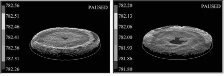
Fig.8.The wafer topography before modifying backing pressure(left)before final CMP(right)after final CMP
By using the modified recipe,we polish some more wafers and the results are shown in Fig.10.As sketched here,the geometry parameters are remarkably improved.Overall,for the 50 wafers polished,there are only 3 wafers being rejected.The acceptance ratio reaches 94%.
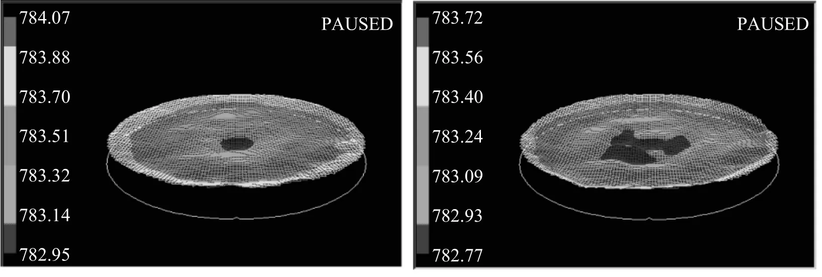
Fig.9.The wafer topography after modifying backing pressure(left)before final CMP(right)after final CMP
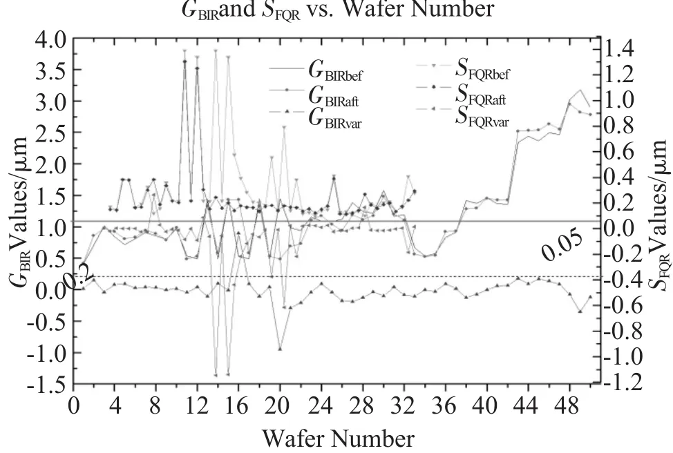
Fig.10.Geometry parameters of Lot 16 to Lot 20
4 Conclusions
In this study,we have performed a qualification check on wafer geometry by using first 300 mm final-touch CMP machine made by us.The objective is to fulfill the requirements of the subsequent 90 nm ULSI manufacturing.For the first batch of wafers(Lot 1 to Lot 10),GBIR and SFQR variation of 82 out of 100 pieces of wafers could fulfill the requirements.However,for the subsequent Lot 11 to Lot 15,the acceptance level drastically drops to 40%.After a thoroughly investigation,we found the deterioration owing to that the incoming wafers are concave thickness diameter profiles.Thanks to our special designed structure of the polishing head,we could modify site backing pressure.As to the concave profile,an edge-fast silicon removal profile should be chosen.Following the suitable pressure distribution of the polishing head,we have improved the polishing results.Finally,corresponding to the demands of 90 nm technology node,we enhance the geometry acceptance level to 94%.
[1] L.C.Zhang,A.Q.Biddut,and Y.M.Ali.Dependence of pad performance on its texture in polishing mono-crystalline silicon wafers[J].Int.J.Mech.Sci.,2010(52):657-662.
[2] E.S.Lee,S.C.Hwang,J.T.Lee,and J.K.Won.A study on the characteristic of parameters by the response surface method in final wafer polishing[J].Int.J.Precis.Eng.Man.,2009(10):25-30.
[3] Y.L.Liu,K.L.Zhang,F.Wang,and W.G.Di.Investigation on the final polishing slurry and technique of silicon substrate in ULSI[J].Microelectron.Eng.,2003(66):438-444.
[4] International Technology Roadmap for Semiconductor 2006 update[Z].Semiconductor Industry Association Report,Sematec Inc.(2006).
[5] M.Forsberg.Effect of process parameters on material removal rate in chemical mechanical polishing of Si(100)[J].Microelectron.Eng.,2009(77):319-326.
[6] H.T.Young,H.T.Liao,and H.Yi.Surface integrity of silicon wafers in ultra precision machining[J].Int.J.Adv.Manuf.Technol.,2006(29):372-378.
