用于3D 集成中的晶圆和芯片键合技术
2010-10-24ShariFarrens
Shari Farrens
(SUSS MicroTec,228 Suss Drive,Waterbury Center,VT 05677,U.S.A.)
1 INTRODUCTION
The basic processing steps that transcend all three stacking options are alignment and bonding.Aligned bonding allows for interlayer connection of TSV’s (through silicon vias)which provide the electrical interconnects.The bonding steps not only provide the mechanical bond between layers but also complete metallurgical reactions that define the resistivity and electrical properties of the connected layers.A variety of choices exist for both alignment and bonding process steps and the following sections will cover in detail these various options.
2 ALIGNMENT STRATEGIES
The TSV size and pitch define the required overlay accuracy needed for substrate alignment and influence bonding choices.Presently the via sizes range from a few micrometers (for IC’s) to 25~50 μm(CMOS image sensors) and the required area overlay is 75%.This sets the limit for post bond alignment accuracy at approximately 1~5 μm.Roadmaps extending out over the next several years point toward submicron alignment requirements for some applications such as stacked IC’s for memory.Figure 1 is one projection provided in the Yole industry report on 3D (1).
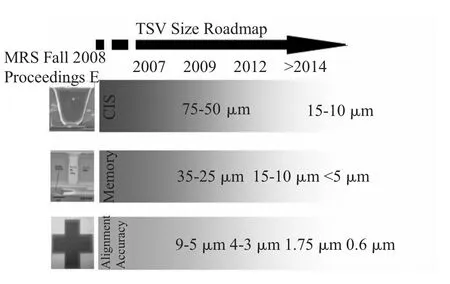
Figure 1 The Through Silicon Via (TSV)size is shown versus production year and the corresponding alignment accuracy need for overlaying the various sized vias.
3 Infrared Alignment
I nfrared alignment uses a light source of approximately 1.2 μm wavelength to transmit the image of the various layers in the substrates to a camera located on the opposite side of the wafer stack.Naturally,metallic layers will appear totally opaque(black) in the final im age since metals totally adsorb the IR wavelengths.Layers with band gaps ≥1.1 eV will be transparent and doped layers will have varying shades of grayscale depending on layer thickness and adsorption coefficient.Due to the interactions with the layers within the wafer and between substrates th e IR technique can be limited as the device and via density increase.In these cases if the IR method is preferred then open areas must be designed around all alignment key positions.The advantage of the IR method is that all the layers are imaged simultaneously.This enables viewing of the active bond alignment process and the results of previous layer stacking.IR alignment is not used in die-to-wafer bonding.
4 Intersubstrate Alignment
Intersubstrate alignment (ISA) uses special optics that are inserted between the two substrates.The left and right objectives image the upper and lower faces of both wafers simultaneously and precision alignment stages bring the wafers into registry.Figure 2 shows the experimental setup for both IR and ISA alignment methods.The benefits of ISA alignment are that the alignment keys placed at the bond interface can be viewed simultaneously.Offsets can be used to accommodate known run out issues and other repeatable errors associated with final alignment accuracy.Historically,precession errors associated with bringing the wafers into proximity and contact after the objectives are retracted,limited the ISA method to roughly ±2 μm accuracy.Recently,precision optics and mechanics have been combined with global inline calibration methods to achieve deep submicron alignment accuracy.Also critical to achieving submicron accuracy is temperature,humidity and vibration control environments such as those used on the SUS S MicroTec BA300UHP precision 3D wafer aligner.
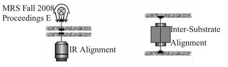
Figure 2 Experimental configuration of IR and ISA alignment.Both methods image fiducials at the bond interface and align to live images rather than stored digital keys.
For Die-to-Wafer bonding the ISA mode is used to align each die on its proper location on the substrate wafer one by one.A single ISA objective is used to scan the wafer surface and identify the proper location and alignment keys on the wafer.Then as each die is picked up the upper ISA objective views its face and the pick-n-place robot brings the die into the correct location.The ISA microscope is retracted and the die are lowered on to the surface and tacked or bonded into location.
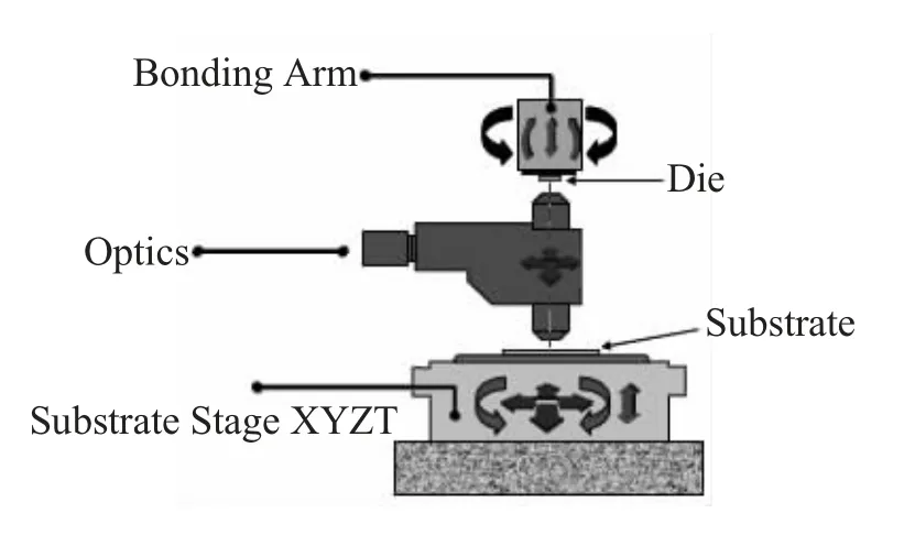
Figure 3 Schematic illustration of Die-to-Wafer alignment and bonding setup.Both the bonding arm and substrate stage control heat.The bond force is applied by the bonding arm.Die-to-wafer alignment accuracy degrade with placement speed but can be in the 1-2 μm range for slower,precision tools such as those illustrated here and offered by SET(2).
5 Alignment Keys
The design of the alignment key also affects the ability to properly align upper and lower substrates.In general non-overlapping keys provide for the most flexibility in use and achieve the best automated results.Cognex has recently recommended the use of Brad fans for use with their automated pattern recognition software (3).The fan itself is an asymmetrical pinwheel in which edge definition software can be used to mathematically define a unique center of mass.When male and female pairs are used the center of the key is exceptionally well defined.Figure 4 shows the
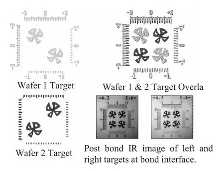
Figure 4.Brad fan design of alignment keys used in 3D integration.The non-overlapping,asymmetric patterns facilitate high resolution overlay placement.The post bond accuracy of the aligned keys in the lower right was submicron as determined by the verniers.
Brad fan design used on the SUSS MicroTec calibration wafers for 300 mm wafer level bonding.The verniers used in this example make use of all four sides of the alignment key by incorporating a coarsely graduated scale on the upper and left sides of the die,and a 0.05 μm scale to the bottom and left side.In this way,x-,y-,and theta misalignments can be calculated.By comparison of radial data from several wafer locations addition data can be harvested to determine thermal expansion contributions and run out errors.These can then be mediated by recipe specific offsets if necessary.
6 WAFER LEVEL BONDING
There are three main wafer bonding methods used in 3D integration;metal to metal diffusion (primarily Cu),silicon direct or fusion bonding,and adhesive (primarily BCB) bonding(4,5).Extensive research activities have been conducted on all these processes and each have advantages and drawbacks to be discussed individually.The primary considerations for 3D integration are alignment accuracy and throughput/cost of ownership.Cost of ownership is often a compromise between meeting device requirements and engineering desires.
6.1 Copper to Copper Diffusion Bonding
The advantage of copper diffusion bonding is that the mechanical as well as electrical connection can be completed simultaneously during the bonding process.The clarity of alignment keys are exceptional when the metal layer incorporates the fiducials and either ISA or IR alignment is appropriate.The drawbacks to copper diffusion bonding are controlling the quality of the copper surfaces and the relatively high temperatures required for the diffusion reaction.
Controlling surface oxidation of copper on the substrates generally involves additives to the chemical mechanical polishing (CMP) slurries and the post-CMP cleaning processes.The copper surface is passivated and oxidation is prevented.The surface passivation layers are removed during heat up in the bonder or by other prebond treatments that are done in batch processing and do not severely impact the process flow.It is also possible to incorporate vapor cleaning processes to remove surface oxidation at point of use in the bond cluster.Using the vapor from formic acid (HC00H) in a bubbler,SUSS MicroTec has developed a point of use removal system for metal oxides.The module is incorporated on the C4NP solder transfer tool and is available for SUSS bond clusters.Figure 5 shows the effect of severe oxide removal using this technique.Wafers are placed in cleaning chambers and exposed to the vapor for a few minutes.The chamber is purged and by controlling the partial pressure of O2in the module no salts are fo rmed that required post process rinses.The process is totally dry and the copper surface is stable for several hours.
这番袒露心声的话,也让我们对金钻明的了解又深了一步。我们本是为太赫兹而想到去找他,而他其实没有太多地涉及现在非常热的太赫兹的各种应用,而是把更多的研究精力放到对太赫兹的基本规律的认识上,并为此乐此不疲。太赫兹辐射技术因为各种安防上的应用而为大众所知,吸引了很多研究力量和资源,而其实揭示其本源和规律同样重要,也更需要有人去做。正是在这一点上,金钻明的工作尤其值得我们称道。
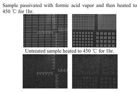
Figure 5 Optical images of device layers heated to 450℃with and without prior surface treatment with formic acid.Dark discoloration is thick copper oxide.
The self-diffusion coefficient for copper is strongly dependent on grain size and dislocation density at low temperatures.This is true for all fcc metals and the effects can be capitalized upon in the case of thin films and copper vias.Figure 6 shows the relationship between the dominant mechanisms for diffusion as a function of normalized temperature(6).The melting point of copper is 1 084℃and with bonding processes ranging from 300~400℃for copper,T/Tmfalls in the range of 0.27~0.36 where defects dominate.In fact,grain boundaries are the primary contributor to atomic motions.
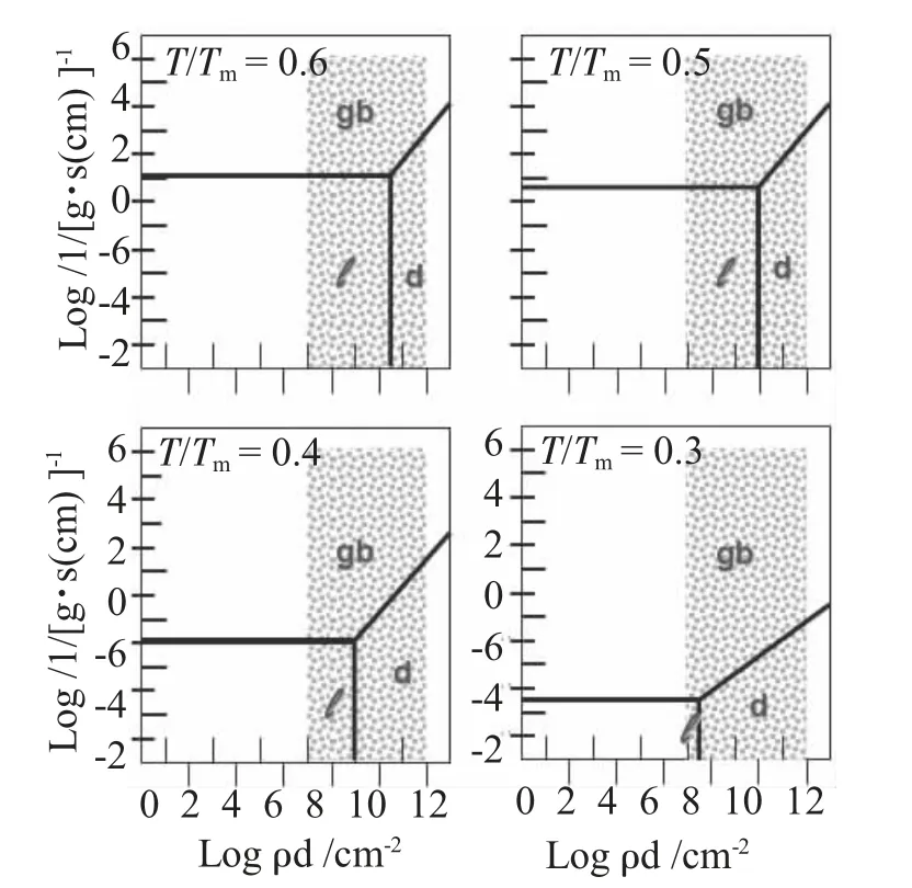
Figure 7.Regimes in which lattice diffusion (l),dislocation diffusion (d)or grain boundary (gb)diffusion dominate the diffusion path.T/Tm is the normalized diffusion temperature where Tm is the melting point of the metal.(6)
Figure 8 is a cross section of a copper via(7).This via is 10 μm wide and several tens of micrometers deep.The SEM image shows how the grain size typically starts submicron at the sidewalls and bottom where the growth initiates from the seed layer.However,the bond interface at the top of the via will typically have grain sizes approaching 2~4 μm.High angle grain boundaries and twins are present extensively throughout copper films and vias.These rapid pathways enhance the low temperature diffusivity and enable copper interconnect technology to occur at semiconductor compatible temperatures.It is,however,difficult to drive the diffusion temperature significantly lower without dramatic alteration of the microstructure with microporous copper deposition or other nonstandard semiconductor deposition/growth methods(8).
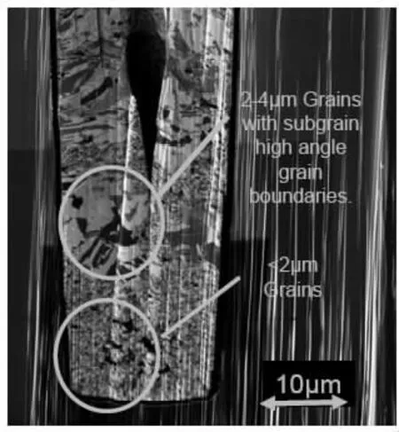
Figure 8 Copper via illustrating grain size and morphology within the via.Oxide liner and seed layer not visible.
7 Fusion Bonding
The most attractive feature of fusion bonding is that the wafers can be room temperature bonded.This has the potential to eliminate one of the contributions to misalignment which is the thermal expansion of one wafer relative to the other during the bond reaction.To put it in perspective a 300 mm silicon wafer with a coefficient of thermal expansion of 3.8×10⁻⁶at 300℃will have grown in diameter by 320 μm.It is imperative that both wafers experience identical temperature profiles to maintain micron level registry between substrates.
The fusion or direct bond process is a two stage kinetic reaction.At room temperature wafers can be aligned and brought into contact.The wafers surfaces have a dipole layer of moisture (water)adsorbed onto the surface that will initially repel the opposite surface.The wafers will“float”above each other until a gentle force,usually a mechanical pin presses lightly at the edge of the wafer.This will overcome the electrostatic repulsion and enable the water molecules to van der Waals bond.The van der Waals forces are weak interactions between the polar water groups with an interfacial energy of<1 J/m2.Wafers can be separated by hand or using a tensile force of nominally 0.1 Pa.However,this bond is sufficient to enable transfer of the aligned and prebonded pairs to annealing furnaces where the bonds can be converted to permanent covalent interfacial bonds.This eliminates many of the thermal expansion problems attributed to the thermal compression bonder used for Cu-Cu diffusion bonds and thermal expansion difference between upper and lower wafers while the bonder is ramped from room temperature to the bond temperature.In other words,for copper bonding there are not attractive forces or low temperature interactions that prevent upper and lower wafers from moving relative to one another until the diffusion reaction initiates.In the fusion bond process the prebond van der Waals attractions are sufficient to hold the wafers in place during the conversion to covalent bonds at elevated temperatures(typically 300℃).
The drawback to fusion bonding is the stringent requirementsfor surface flatnessandroughness.Becausethe vander Waalsbonds areweakinteractionsit isnot possible to prebond wafers with roughness values>1 nm RMS or withbow/warplevelsinexcessiveof~50μm.Fusionbondingfor 3Dhasbeenmost successful whenthe device layers are passivated byblanket layers of dielectric material such asPECVDoxideorotherlowtemperatureoxidelayers.
The passivation layer is easily CMP’d and resulting surfaces are of sufficient quality to enable fusion bonding.However,there are no direct electrical connections across the interface to interconnect the metal layers.Additional processing is therefore required to etch through the wafer stack and backfill vias with metals.This is done by thinning one of the substrates to several tens of micrometers and follow by a patterned etch and metal backfill in a process known as“via last”processing.
More recently hybrid technology is being investigated in which the vias are buried below a dielectric blanket layer and the CMP process goes beyond planarizing the oxide and exposes the surfaces of the metal plugs.Care must be taken to control the dishing and conversely the crowning of the metal with respect to the passivation layer.However,results are emerging that indicate this technique may be applicable to production process flows.Ziptronix has developed many of these processes and the reader is referred to this literature for details (9).These methods could enable via first processing using hybrid fusion bonding.
Fusion bondinghas resulted in consistent submicron alignment accuracies whenever the bonding requirements can be fulfilled.Certainly as CMP processes improve this technique will find full scale productionvalue.
7.1 Adhesive Bonding for 3D
Adhesive bonding for 3D falls in the intermediate range with respect to temperature.BCB (benzocyclobutene) is the most often used polymer for precision 3D adhesive bonding and is bonded from 150-320℃.By controlling the rheology of the film during the precure step the material can be manipulated to customize the interfacial compliancy and provide low temperature bonding and alignment accuracies in the 1~2 μm range.Extensive literature about BCB bonding for use in 3D applications exists and illustrate process flows for front to front or front to back stacking sequences.The general process flow starts with the application of BCB to one or both of the surfaces.When one wafer only is coated it is important to use adhesion promoter AP3000 on the opposing side.Typical total thicknesses are~2 μm.Figure 9 shows the evolution of the bonded BCB layer if the precure (bake out step before bonding)is not sufficient to remove all the residual solvents.Basically,for precuring below 150℃there is an almost certain chance that the film will dissociate resulting in poor bond integrity.All precure conditions for this figure were for 1 hr and final bonds were done at 250℃.
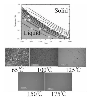
Figure 9 The phase diagram for BCB in the upper portion of the figure shows the transition from liquid to solid.The lower figures show the final film structure for various one hour pre-cure temperatures before alignment and bonding at 250℃.
Other polymers have been identified as candidates for 3D integration application but thus far none have been adopted.BCB has certain drawbacks with cost and inter-via connections must be made after bonding and thinning.There is presently no commercial activity for BCB in 3D integration but some use in CMOS image sensors for high end applications in digital cameras.
Table 1 summarizes the advantages and disadvantages of the three bonding techniques discussed for 3D applications.At this time the only applications in production are CMOS image sensor.These products use both the metal bonding technology utilizing Cu TSV’s and also the fusion bonding techniques at wafer level.
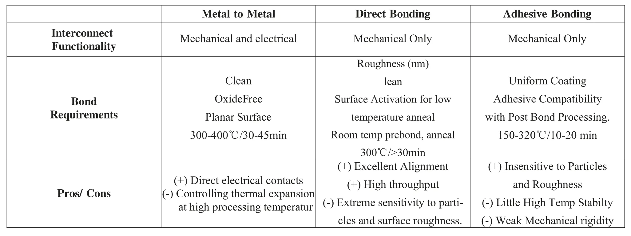
Table I Comparison of Wafer Level Bonding Technologies for 3D Integration
8 DIE-TO-WAFER BONDING
Wafer level bonding only applies when the substrates are matched materials type,when die sizes are the same,and when both wafers have excellent yield.Thus die-to-wafer bonding is extensively used for heterogeneous integration and for mixed signal processes.It is also very useful and attractive for assembly of more than one size die onto the wafer and irregular population of the wafer.
Figure 10 graphically illustrates the bottom-line in die-to-wafer vs.wafer-to-wafer choices.The placement of die is not simultaneously accurate and fast.A typical pick and place die bonder may do several 100’s or more of placements but with an accuracy of>10 μm.A precision die bonder such as the SET FC250 can achieve micron level alignment but may take over 1 hour to populate the wafer.Thus figure 10,accurately illustrates that when you have many small die which is synonymous with a large number of die to place,and you want a high degree of placement overlay then the wafer to wafer techniques are superior choices.The die bonder is inefficient and limited in abilities to perform advanced metallurgical bonds that require high temperatures or force.Since the placement of the die is already a throughput bottleneck if the desired bond is copper to copper diffusion process there are significant issues.Among the primary ones are how to heat to 300~400℃for several minutes

Figure 10 Approximate cost as a function of die size and placement accuracy for C2W and W2W bonding technology(1).
under a relatively high force without heating surrounding wafer locations.Thus many die-towafer scenarios use low temperature eutectic alloys to tack the wafers in location and then move the populated wafer to a thermal compression bonder to apply high force and high heat to all die at the same time.The solder is consumed in the diffusion reaction and if properly controlled the reflow of the solder will not degrade the alignment accuracy too severely.There are similar uses of polymers for temporary tacking of the die to the main substrates as well.
9 SUMMARY
Both wafer level and die-to-wafer bonding will be used in 3D integration.The economic benefit of wafer-to-wafer bonding applies primarily to small die size or very dense interconnects in which a high alignment accuracy is required.Wafer level bonding is a applicable to bonding of same size die and wafers from which the yields are both very high.Die-to-wafer bonding is preferred for mixed processes and is very economical for larger die that require >2 μm overlay accuracy.Perhaps,for some products the compromise will come in the form of die-to-wafer population and populated wafer thermal compression bonding as a second step.
There is no production of 3D devices on the market and R&D activities continue to home in on viable high volume solutions.Equipment suppliers are meeting and exceeding roadmap requirements with new wafer level bonding options as the technology matures to a production worthy manufacturing option.
[1]Yole 2007 MEMS Industry Report[B/OL].http://www.yole.fr/pagesAn/products/report_MEMS.asp
[2]http://www.set-sas.fr/en/multipage.xml?pg=1&id=173582.[Z]
[3]Bill Silver,“The evaluation and design of a Universal Alignment Target”,[C].rev 2.0,March 12,2000.
[4]Chuan Seng Tan,Ronald J.Gutmann and L.Rafael Reif,”Wafer Level 3-D IC’s Process Technology”[C].(Springer,New York,2008).
[5]Phil Garrou,“Handbook of 3D Integration”[C].(Wiley,Weinheim Germany,2008).
[6]D.Gupta,D.R.Campbell,and P.S.,Chapter 7“Grain Boundary Diffusion”[C].Thin Films Interdiffusion and Re actions edited by J.M.Poate,K.N.Tu and I.W.Mayer,(Wiley,New York,1978)p.164.
[7]Courtesy of STS[Z].
[8]Pei-I Wang et.al.,“Low Temperature Copper-Nanorod Bonding for 3D Integration”[C].(Mater.Res.Soc.Symp.Proc.970,Pittsburg,PA,2007).
[9]Paul Enquist,“Direct Bond Interconnect (DBI.) -Technology for Scaleable 3D SoCs”[C].(RTI Conference Proceedings on Semiconductor Integration and Packaging Accessing Technological Developments,Applications,and Key Enablers,Marriot San Francisco Airport Hotel,Burlingame,California,Oct.31-Nov.2,2006).