Effect of annealing on the electrical performance of N-polarity GaN Schottky barrier diodes
2024-04-23NuoXuGaoqiangDengHaotianMaShixuYangYunfeiNiuJiaqiYuYusenWangJingkaiZhaoandYuantaoZhang
Nuo Xu, Gaoqiang Deng, Haotian Ma, Shixu Yang, Yunfei Niu, Jiaqi Yu, Yusen Wang, Jingkai Zhao,and Yuantao Zhang
State Key Laboratory of Integrated Optoelectronics, College of Electronic Science and Engineering, Jilin University, Changchun 130012, China
Abstract: A nitrogen-polarity (N-polarity) GaN-based high electron mobility transistor (HEMT) shows great potential for high-frequency solid-state power amplifier applications because its two-dimensional electron gas (2DEG) density and mobility are minimally affected by device scaling.However, the Schottky barrier height (SBH) of N-polarity GaN is low.This leads to a large gate leakage in N-polarity GaN-based HEMTs.In this work, we investigate the effect of annealing on the electrical characteristics of N-polarity GaN-based Schottky barrier diodes (SBDs) with Ni/Au electrodes.Our results show that the annealing time and temperature have a large influence on the electrical properties of N-polarity GaN SBDs.Compared to the N-polarity SBD without annealing, the SBH and rectification ratio at ±5 V of the SBD are increased from 0.51 eV and 30 to 0.77 eV and 7700, respectively, and the ideal factor of the SBD is decreased from 1.66 to 1.54 after an optimized annealing process.Our analysis results suggest that the improvement of the electrical properties of SBDs after annealing is mainly due to the reduction of the interface state density between Schottky contact metals and N-polarity GaN and the increase of barrier height for the electron emission from the trap state at low reverse bias.
Key words: nitrogen polarity; GaN; Schottky barrier diodes; annealing; interface state
1.Introduction
GaN-based high electron mobility transistors (HEMTs)have important applications in wireless communications,phased array radar and other fields because of the high twodimensional electron gas (2DEG) density and mobility[1,2].The device structure of a GaN-based HEMT grown along thec-axis has two polarities: metal-polarity and nitrogen-polarity(N-polarity).Among them, metal-polarity HEMTs are widely used and studied.However, compared with metal-polarity HEMTs, N-polarity HEMTs have more advantages in high-frequency applications.The device structure of a N-polarity HEMT differs from that of a metal-polarity HEMTs, and its 2DEG channel is located on the GaN side near the gate.Generally, to realize high-frequency operation, the scaling of a HEMT structure is required.For a N-polarity HEMT, the 2DEG density and mobility hardly change with device dimension scaling[3-6].Therefore, a high output power can be maintained at a high operating frequency.However, for a metal-polarity HEMT, the 2DEG channel is located on the GaN side below the AlGaN barrier.Its 2DEG density decreases rapidly with device dimension scaling, which makes it difficult to realize high output power at a high operating frequency.In addition, a N-polarity HEMT enables a low Ohmic contact resistance and a stronger confinement of 2DEG in the channel[7,8].In 2011, Brownet al.reported the fabrication of high-performance N-polarity HEMTs with a output power of 1.5 W/mm and a maximum power-added efficiency of 24.2% at 94 GHz[9].In 2018, the output power of the N-polarity HEMT reaches 7.94 W/mm at 94 GHz, which is about two times the output power of the metal-polarity HEMT in the W-band at that time[10].However, the Schottky barrier height (SBH) of Npolarity GaN is low and thus the reverse leakage is relatively high, which affects the performance of N-polarity HEMTs[11-14].This is mainly because of the higher background electron concentration and the reversal polarization field of N-polarity GaN compared to that of metal-polarity GaN[13,15-18].Researchers currently solve this problem mainly by introducing an insulating layer between the gate metal and N-polarity GaN to form a metal—insulator—semiconductor (MIS) structure[18-20].However, this method increases the distance from the gate to the channel, and thus reduces the gate control capability of N-polarity HEMTs.Meanwhile, this method makes the device process more complex.
In this work, we studied the effect of the annealing process of the Schottky contact electrode (Ni/Au) on the electrical characteristics of N-polarity GaN Schottky barrier diodes(SBDs).In an N-polarity GaN-based SBD, the properties of Schottky contact to N-polar GaN can be well evaluated.Our results show that with the optimized annealing process the electrical characteristics of N-polarity SBD can be improved effectively.An SBD with a higher SBH and rectification ratio,and a lower ideal factor can be achieved by annealing.Moreover, our analysis suggests that the improvement of device performance after annealing is mainly owing to the reduction of the density of the interface state between the Schottky contact metals and the N-polarity GaN, and the increase of barrier height for the electron emission from the trap state at low reverse bias.This work provides a simple and feasible way to obtain high-quality Schottky contacts on N-polarity GaN for N-polarity GaN HEMTs.
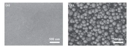
Fig.1.Surface SEM images of GaN film (a) before and (b) after KOH etching.
2.Experimental procedure
All N-polarity GaN films are grown on sapphire substrates using an Aixtron CCS 3 × 2ˊˊ FT metal organic chemical vapor deposition (MOCVD) system.Prior to the growth,the substrate is thermally cleaned at 1060 ℃ for 5 min in the H2atmosphere.Then, the growth begins with a low-temperature GaN nucleation layer grown at 570 ℃.After that the growth temperature is ramped up to 1060 ℃ to grow a 2-μm-thick high-temperature GaN film.After the growth, we performed wet etching experiments to verify the lattice polarity of GaN[21,22].Figs.1(a) and 1(b) show the surface scanning electron microscopy (SEM) image of the GaN film before and after etching with 8 mol/L KOH at 40 ℃ for 5 min.It is obvious that the obtained GaN film can be etched by KOH, indicating that its lattice polarity is N-polarity.The crystalline quality and surface morphology of the N-polarity GaN can be found in our previous work[23].The crystalline quality of the N-polarity GaN in our work is comparable to that of metalpolarity GaN, as shown in Table 1.But the background electron concentration (ND) of N-polarity GaN is higher than that of metal-polarity GaN (Table 1) due to the stronger bonding of oxygen atoms on the N-polarity surface[17].

Table 1.Characterization of nominally undoped metal-polarity and N-polarity GaN.
Then, we fabricated SBD devices based on the prepared N-polarity GaN films.Prior to the device process, all N-polarity GaN films were ultrasonically cleaned using acetone,ethanol and deionized water.After that, the SBD devices were prepared by a standard lithography process.The schematic diagram of a N-polarity SBD device is shown in Fig.2(a).The Ohmic contact metals of SBD devices were Ti/Al/Ni/Au (20/100/40/50 nm) stack metals deposited by electronic beam evaporation.To form Ohmic contacts, contact metals were annealed at 770 ℃ in N2atmosphere for 15 s.After the Ohmic contact process is finished, Ni/Au (20/40 nm)Schottky contact metals were deposited.To investigate the effect of the annealing process of Schottky contact metals on the device performance, Schottky contact metals under the same deposition conditions were annealed with different times and temperatures.Fig.2(b) shows the surface optical microscope (OM) image of an SBD device, where the diameter of the Schottky contact electrode is 140μm.After the devices were prepared, current-voltage (I-V) characteristic and capacitance-voltage (C-V) characteristic curves of these devices were recorded by a keysight B2902A precision-type source meter and a keysight B1500A semiconductor device analyzer, respectively.Noting that the SBH, rectification ratio,ideal factor, and the density of interface state between Schottky contact metals and GaN of an SBD device can be calculated and analyzed by itsI-Vcharacteristic curve.

Fig.2.(Color online) (a) The schematic structure of N-polarity GaNbased SBD.(b) Surface OM image of a fabricated N-polarity GaNbased SBD.
3.Results and discussion
3.1.Effect of annealing time on the electrical properties of N-polarity GaN SBD devices
Firstly, we fabricated four N-polarity GaN SBD devices with various annealing times (30 , 60 , 120 , and 240 s) but a constant annealing temperature of 450 ℃.In addition, we also fabricated a N-polarity GaN SBD device without annealing for comparison.The current density-voltage (J-V) curves of these devices are shown in Fig.3.The relationship betweenJandIis:

Fig.3.(Color online) J-V curves of SBD devices with different annealing times in (a) linear scale and (b) semilog scale.(c) lnI-V curve of the SBD device with an annealing time of 60 s.
whereAis the area of the Schottky contact electrode.Fig.3(a) shows theJ-Vcurves in linear scale for these SBDs with different annealing times, from which the turn-on voltages (Von) of SBD devices with different annealing times can be extracted.The results show that with the increase of annealing time, theVonof SBD devices first increases and then decreases.The device with an annealing time of 60 s has the highestVonof 0.78 V.Fig.3(b) shows theJ-Vcurves in semilog scale, which provides a clearer view of the reverse leakage current density of each device.We can see that the SBD device without annealing has the highest leakage current density of 73 A/cm2at -5 V.After annealing, the reverse leakage current density of the SBD device decreases significantly.At an annealing time of 60 s, the SBD device has the lowest reverse leakage current density of 0.34 A/cm2at -5 V.
TheI-Vcharacteristic curve of a SBD device can be analyzed with the standard thermionic emission theory[24,25]:
At a forward biasV>3kT/q, Eq.(1) can be simplified as:
Taking the natural logarithm on both sides of the equation:
whereqis the absolute value of the electron charge,nis the ideal factor,kis the Boltzmann's constant,Tis the test temperature.AndIsis the reverse saturation current, it can be expressed as follows[24,25]:
whereφBis the SBH andA* is Richard's constant.The expression ofA* is as follows[26]:
wherem* is the electron effective mass of GaN (m* = 0.22 ×m0[27],m0is the free electron mass), andhis Planck's constant.Fig.3(c) shows the lnI-Vcurve of the SBD with an annealing time of 60 s.The lnI-Vcurve is fitted with Eq.(4),as plotted with red dotted line shown in Fig.3(c).It can be seen from Eq.(4) that the slope of the dotted line isq/nkT.Therefore, an ideal factor of 1.54 is obtained.The intercept of the dotted line from the longitudinal axis is lnIs.As a result,the SBH value of 0.77 eV is calculated with Eq.(5).
Fig.4 shows the calculated ideal factor, SBH, and rectification ratio (Ion/Ioff) at ±5 V for SBD devices with different annealing times, where the rectification ratio provides a better representation of the reverse leakage current.After annealing, the SBH of SBD devices is increased, and the ideal factor is reduced, as shown in Fig.4(a).The SBD device has a higher SBH and a lower ideal factor at an annealing time of 60 and 120 s.In addition, as can be seen from Fig.4(b), the rectification ratios of SBD devices are improved after annealing, and the SBD with an annealing time of 60 s has the largest rectification ratio of 7700.This means that the reverse current leakage of a GaN SBD is greatly suppressed.In addition, the ideal factor greater than one may be due to the presence of natural oxides on the surface of GaN or the inhomogeneous of the Schottky barrier[28].
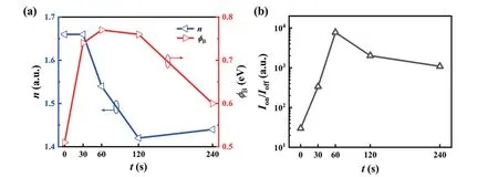
Fig.4.(Color online) (a) Ideal factor and SBH of SBD devices with different annealing times.(b) Rectification ratios at ±5 V of SBD devices with different annealing times.
The difference of the SBH values between the SBDs with an annealing time of 60 and 120 s is small (0.01 eV), however,the difference in rectification ratios between these two devices is large (5700).This indicates that the reduction of reverse leakage current is not completely dependent on the rise of the SBH.This is because the reverse leakage current is also related to the interface states between the contact metals and GaN surface, and the SBH can also be affected by Fermi level pinning effect[29].The above analysis results show that Schottky contacts with good electrical characteristics can be achieved on N-polarity GaN by annealing at 450 ℃ for 60 s.
3.2.Effect of annealing temperature on the electrical properties of N-polarity GaN SBD devices
Based on the optimized annealing time of 60 s, we fabricated another four N-polarity GaN SBD devices with various annealing temperatures (300, 375, 525, and 600 ℃).Fig.5(a)shows the linear scaleJ-Vcurves of these SBD devices.TheJ-Vcurve of the SBD device with an annealing temperature of 450 ℃ is also plotted in Fig.5(a).We can see that theVonof the SBD device increases and then decreases with the annealing temperature, and theVonis the largest when the annealing temperature is 450 ℃.Fig.5(b) shows the semilog scaleJ-Vcurves of these SBD devices.and it can be clearly observed that the reverse leakage current density of the device decreases and then increases with the annealing temperatures.At the annealing temperature of 450 ℃, the SBD has the lowest reverse leakage current density.Further increasing the annealing temperature to 600 ℃, the device reverse leakage current density increases dramatically and is higher than that of the SBD device without annealing.This is mainly because the high annealing temperature enhances the interaction between GaN and the contact metals[30,31].

Fig.5.(Color online) J-V curves of SBD devices with different annealing temperatures in (a) linear scale and (b) semilog scale.
Fig.6 shows the calculated ideal factor, SBH, and rectification ratio at ±5 V for SBD devices with different annealing temperatures.We can see that the SBD device with an annealing temperature of 450 ℃ has the best electrical characteristics,it has an SBH of 0.77 eV and a rectification ratio of 7700 at±5 V, while it has an ideal factor of 1.54.At -1 V, its leakage current density is 1.9 × 10⁻⁵A/cm2, as shown in Fig.5(b).The performance of this SBD device is comparable to that of recently reported N-polarity GaN SBD with a SiN interlayer between the Schottky contact metals and N-polarity GaN (SBH: 0.8 eV; reverse leakage current density at -1 V:~10-5A/cm2)[18].This indicates that the electrical properties of the Schottky contacts to N-polarity GaN can be improved effectively by optimizing the annealing process.
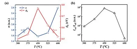
Fig.6.(Color online) (a) Ideal factor and SBH of SBD devices with different annealing temperatures.(b) Rectification ratios at ±5 V of SBD devices with different annealing temperatures.
3.3.Analysis on the interface states between Schottky contact metals and N-polarity GaN
To reveal the influence mechanism of annealing process on the electrical characteristics of SBD devices, we studied the interface characteristics between the Schottky contact metals and N-polarity GaN onI-Vcurves.The density of interface state (NSS) between the Schottky contact metals and Npolarity GaN can be calculated according to Card and Rhoderick’s method[32]:
whereεiis the relative permittivity of the thin oxide dielectric layer between GaN and Schottky contact metals,δis the thickness of this dielectric layer.The values ofεiandδdo not affect the comparative analysis of the density of interface state.Here,εi= 7ε0,δ= 1 nm are adopted for calculation[28].ε0is the vacuum permittivity.εsis the permittivity of the GaN.WDis the space charge region width on the GaN side.WDis defined as follows:
whereNCis the conduction band state density of GaN.n(V) is the voltage-dependent ideal factor function and it can be defined as follows[33]:
Then, the energy distribution of the interface states can be estimated withn(V) and the effective SBHφe[34]:
whereESSis the energy of the interface states andEC-ESSis the position of the interface state energy at the interface relative to the conduction band.Based on the above equations,we obtain the relationship curves betweenNSSandEC-ESSfor SBD devices with different annealing process, as shown in Figs.7(a) and 7(b).It can be observed from Fig.7(a) that the density of interface state of SBD device without annealing are higher, between 2 × 10¹³eV-1·cm-2and 4 × 10¹³eV-1·cm-2.Meanwhile, the interface state densities are decreased after annealing, as shown in Fig.7(a).However, the density of interface state (between 4 × 10¹³eV-1·cm-2and 1.2 ×10¹⁴eV-1·cm-2) of the device with an annealing temperature of 600 ℃ is higher than that of the device without annealing,as shown in Fig.7(b).At an optimized annealing process(450 ℃ for 60 s), the density of interface state is reduced to a relatively low value, and thus the SBD device has a lower ideal factor and a reverse leakage current density as well as a higher SBH.
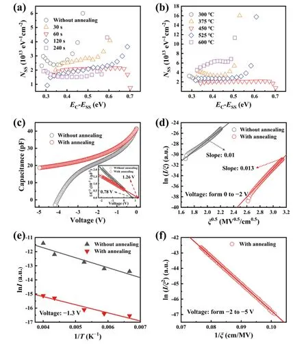
Fig.7.(Color online) The relationship curves between NSS and EC-ESS for SBD devices with different annealing (a) times and (b) temperatures.(c)C-V and 1/C2-V curves, (d) ln(I/ξ)-ξ0.5 curves and (e) lnI-1/T curves of the SBD devices without and with annealing at 450 ℃ for 60 s.(f)ln(I/ξ2)-ξ-1 curve of the SBD device with annealing at 450 ℃ for 60 s.
3.4.Analysis on current leakage mechanism of Npolarity GaN SBD devices
Moreover, we analyzed the current leakage mechanism of N-polarity GaN SBD devices, because the SBH and the current leakage of an SBD is also strongly dependent on its current leakage mechanism.The current leakage mechanism of the SBD devices can be investigated by Poole-Frenkel emission (PFE) model and Fowler-Nordheim (FN) tunneling model.Among them, PFE model is a temperature-dependent leakage current mechanism at a weak electric field, and its leakage currentIPFcan be defined as follows[35]:
whereZisaconstant,φtisthebarrierheightforthe electron emission fromthetrap state andεsh=5.8ε0isthe permittivity of the semiconductor at high frequency.The electric field (ξ) of the Schottky contact can be calculated from the results ofC-Vmeasurement[36]:
whereVbiis built-in voltage.The measuredC-Vcurves under reverse bias for SBD devices without and with annealing at 450 ℃ for 60 s are shown in Fig.7(c).The values ofVbifor SBD devices without and with annealing can be extracted from the 1/C2-Vcurve[12], which are 0.78 and 1.26 V, respectively, as shown in the inset of Fig.7(c).In addition, it can be found that theCof the SBD device without annealing shows an unusual decay at the voltage range from -2 to -5 V, and decreases to negative values at the voltage around —4 V,which may be due to the high density ofNSS[37,38].Based on theI-VandC-Vmeasurement results, we obtain the ln(IPF/ξ)-ξ0.5curves for these two SBD devices in the low reverse bias range from 0 to -2 V, as shown in Fig.7(d).We can see that ln(IPF/ξ) andξ0.5for both SBD devices are approximately linearly related.The fitted slopes of the ln(IPF/ξ)-ξ0.5curves for the SBD devices without and with annealing are 0.01 and 0.013, respectively, which are close to the theoretical value of 0.012 calculated based on Eq.(13).This suggests that the PFE is the main current leakage mechanism at low reverse bias.Fig.7(e) shows the measured lnI-1/Tcurves for the SBD devices without and with annealing at 450 ℃ for 60 s at temperatures ranging from 150 to 250 K at -1.3 V.We can see that lnIis linearly related to 1/T, which is consistent withEq.(13).ThefittedφtoftheSBDdeviceswithoutand withannealing are0.13 and0.42eV,respectively.Therefore,it is suggested that the optimized annealing process raisesφt,which leads to the reduction in the leakage current.
In addition, we analyze the current leakage mechanism for these two SBD devices at higher reverse bias.The current leakage mechanism at strong electric field can be studied by the temperature-independent FN tunneling model.In this model, the leakage currentIFNcan be defined as follows[39]:
whereDis a constant, andBcan be expressed as[39]:
Fig.7(f) shows the ln(IFN/ξ2)-ξ-1curves of the SBD device with annealing at 450 ℃ for 60 s.The ln(IFN/ξ2)-ξ-1curve of SBD device without annealing is not shown in Fig.7(f)because itsC-Vcurve shows an unusual decay at bias greater than -2 V, as shown in Fig.7(c).We can see from Fig.7(f) that ln(IFN/ξ2) andξ-1are approximately linearly related, which is consistent with Eq.(16).This suggests that the FN tunneling is the main current leakage mechanism at higher reverse bias.
To understand the effect of annealing process on the current leakage of N-polarity SBD devices intuitively, we plot the schematic energy band diagrams of SBD devices without and with annealing at 450 ℃ for 60 s, respectively, as shown in Fig.8.As we mentioned above, the density of interface states of SBD devices without annealing is higher than that with annealing at 450 ℃ for 60 s.Meanwhile, it is worth noting that the energy of the interface states is close to the conduction band edge, as shown in Figs.7(a) and 7(b).Therefore, wecan infer that these interface states above the Fermi level would be positively charged due to the ionization, and the density of the positive interface charges of the SBD device without annealing is higher than that with annealing.This means that the SBD device without annealing has a lower SBHφBcompared to the SBD device with annealing.As we marked in Figs.8(a) and 8(b), the values of SBHφBfor the SBD devices without and with annealing are 0.51 and 0.77 eV, respectively, according to our calculation results shown in Fig.4(a) and Fig.6(a).In addition, the schematic diagrams of current leakage under FN model and PFE model are also plotted in Fig.8.The barrier heightφtfor the electron emission from the trap state of the SBD device with annealing (0.42 eV) is higher than that of the SBD device without annealing (0.13 eV), according to the fitting results mentioned above.Therefore, from the energy band diagram, we can see intuitively that the SBD device with annealing has a lower reverse leakage current compared with the SBD device without annealing due to the higher SBH andφt.
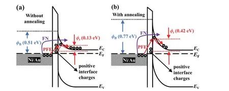
Fig.8.(Color online) The energy band diagrams of Schottky contact region for SBD devices (a) without annealing and (b) with annealing at 450 ℃ for 60 s.
Lastly, to facilitate the understanding of the physical notations in this work, we list some of the main physical notations and their corresponding physical names in Table 2.
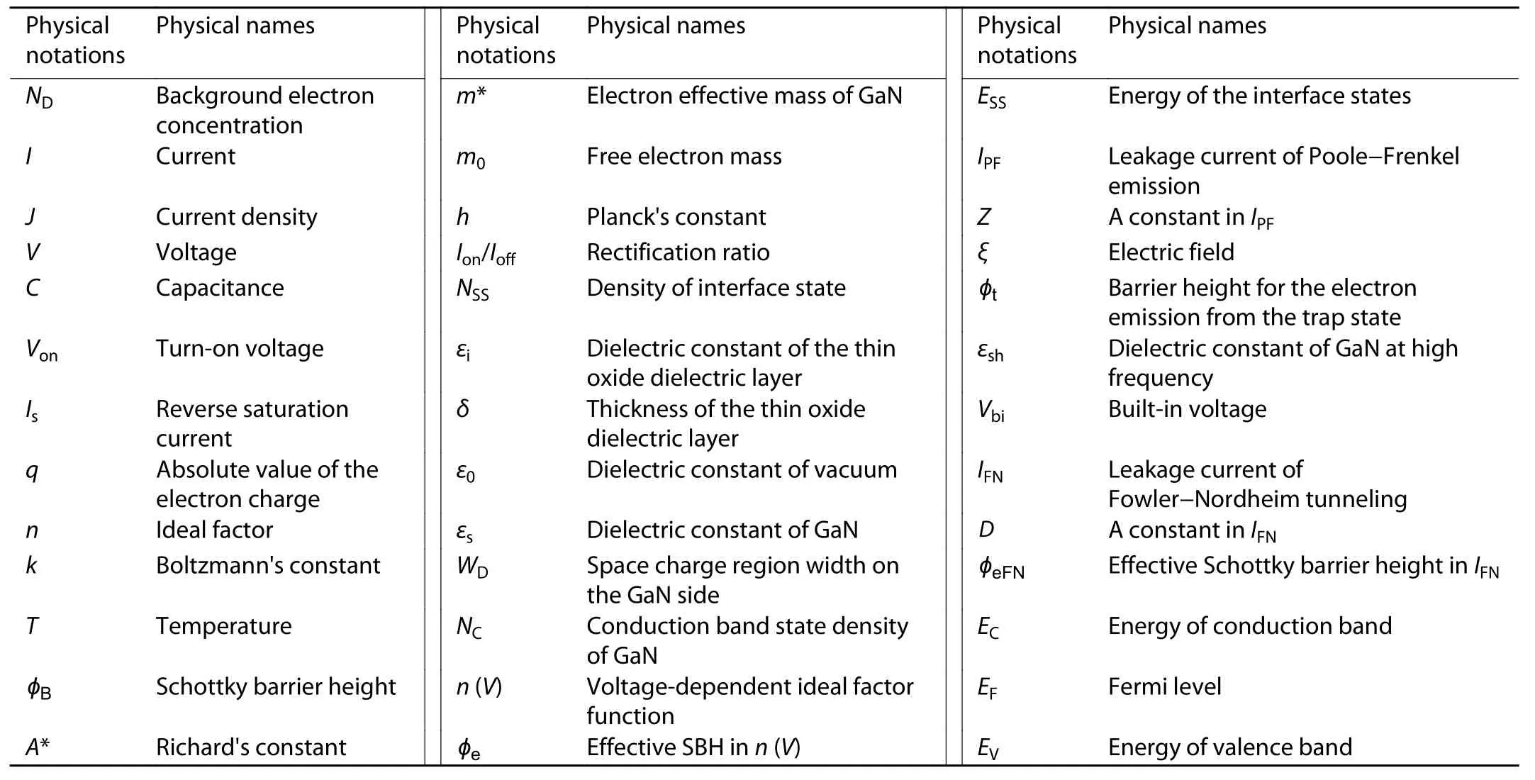
Table 2.Physical notations used in this work and corresponding physical names.
4.Conclusion
In summary, we have grown N-polarity GaN films by MOCVD and fabricated N-polarity GaN SBD devices through the photolithography and metal deposition process.Importantly, we studied the influence of the annealing process of Schottky contact metals on the electrical performance of SBD devices.Our results show that the annealing treatment is conducive to improve the SBH, and reduce the ideal factor and reverse leakage current density of the SBD device.This is mainly because annealing can reduce the density of interface state between Schottky contact metals and the N-polarity GaN and increase the barrier height for the electron emission from the trap state, but too high an annealing temperature will greatly increase the density of interface state and seriously degrade the electrical properties of the SBD device.It is reasonably believed that this work provides a feasible way to realize high-quality Schottky contacts on N-polarity GaN for N-polarity GaN-based HEMTs.
Acknowledgements
This work was supported by the National Key R & D Program of China (Nos.2022YFB3605205, 2021YFB3601000, and 2021YFB3601002), the National Natural Science Foundation of China (Nos.U22A20134, 62074069, 62104078, and 62104079), and the Science and Technology Developing Project of Jilin Province (Nos.20220201065GX,20230101053JC, and 20220101119JC).
杂志排行
Journal of Semiconductors的其它文章
- Chemical vapor deposition for perovskite solar cells and modules
- Highlights in recent wireless power IC research
- Recent advancements in continuously scalable conversion-ratio switched-capacitor converter
- Towards efficient generative AI and beyond-AI computing:New trends on ISSCC 2024 machine learning accelerators
- Millimeter-wave PA design techniques in ISSCC 2024
- Light-emitting devices based on atomically thin MoSe2
