Light-emitting devices based on atomically thin MoSe2
2024-04-23XinyuZhangXuewenZhangHanweiHuVanessaLiZhangWeidongXiaoGuangchaoShiJingyuanQiaoNanHuangTingYuandJingzhiShang
Xinyu Zhang, Xuewen Zhang, Hanwei Hu, Vanessa Li Zhang, Weidong Xiao, Guangchao Shi,Jingyuan Qiao, Nan Huang, Ting Yu,3,†, and Jingzhi Shang,†
1Institute of Flexible Electronics, Northwestern Polytechnical University, Xi'an 710129, China
2School of Physics and Technology, Wuhan University, Wuhan 430072, China
3Wuhan Institute of Quantum Technology, Wuhan 430206, China
Abstract: Atomically thin MoSe2 layers, as a core member of the transition metal dichalcogenides (TMDs) family, benefit from their appealing properties, including tunable band gaps, high exciton binding energies, and giant oscillator strengths, thus providing an intriguing platform for optoelectronic applications of light-emitting diodes (LEDs), field-effect transistors (FETs), single-photon emitters (SPEs), and coherent light sources (CLSs).Moreover, these MoSe2 layers can realize strong excitonic emission in the near-infrared wavelengths, which can be combined with the silicon-based integration technologies and further encourage the development of the new generation technologies of on-chip optical interconnection, quantum computing, and quantum information processing.Herein, we overview the state-of-the-art applications of light-emitting devices based on twodimensional MoSe2 layers.Firstly, we introduce recent developments in excitonic emission features from atomically thin MoSe2 and their dependences on typical physical fields.Next, we focus on the exciton-polaritons and plasmon-exciton polaritons in MoSe2 coupled to the diverse forms of optical microcavities.Then, we highlight the promising applications of LEDs, SPEs, and CLSs based on MoSe2 and their heterostructures.Finally, we summarize the challenges and opportunities for high-quality emission of MoSe2 and high-performance light-emitting devices.
Key words: MoSe2; light-matter interaction; exciton; polariton; light-emitting device
Citation:X Y Zhang, X W Zhang, H W Hu, V L Zhang, W D Xiao, G C Shi, J Y Qiao, N Huang, T Yu, and J Z Shang, Light-emitting devices based on atomically thin MoSe2[J].J.Semicond., 2024, 45(4), 041701.https://doi.org/10.1088/1674-4926/45/4/041701
1.Introduction
Two-dimensional (2D) TMDs have recently received considerable attention owing to their exceptional optoelectronic properties and have become a hot research topic in 2D materials fields.In the emerging class of atomically thin TMDs, MoS2, WS2, MoSe2, and WSe2are typical representatives with similar band structures and van der Waals (vdW) layered structures[1,2].Among them, MoSe2, as an essential member of the TMDs family, benefits from the narrower linewidth,lower band gap energy, and higher electron mobility compared with the extensively investigated MoS2.Therefore,MoSe2emerged as an intriguing platform in the applications of LEDs[3], FETs[4], and other optoelectronic devices[5], as presented in Fig.1.Importantly, as a direct band gap semiconductor, monolayer MoSe2possesses merits such as high exciton binding energy, giant oscillator strength, and easy integration[6], leading to itself as a promising gain medium for the integration of 2D semiconductor lasers with both high emitting performance and low power consumption.Moreover,atomically thin MoSe2can realize the emission behavior of neutral excitons in the near-infrared wavelength, which could be combined with the silicon-based integration technology and further give rise to flourishing the new generation of on-chip optical interconnection, quantum computing, and quantum information processing.On the other hand, the exciton emission behavior of atomically thin MoSe2is tunable and can be modulated by external physical conditions, such as temperature, substrates, and applied physical fields.Beyond individual atomically thin MoSe2, MoSe2can be stacked with different vdW materials to construct novel heterostructures by vdW interactions, including h-BN/MoSe2/h-BN[7], h-BN/MoSe2/WS2/h-BN[8], and MoSe2/WSe2[9].In addition, MoSe2or other TMDs can be stacked with many other 2D materials,such as InSe[10,11], 2D perovskites[12-14], etc.to form vdW heterostructures with fascinating properties, such as bias tunable spectrum, robust interlayer coupling, valley pseudospin,and interlayer excitons.These heterostructures exhibit peculiar physical properties, which provide a desirable platform to investigate the exciton states, light-matter coupling effects,and carrier dynamics.The interlayer excitons are formed by electrons and holes, localizing in different layers of the heterostructures[15].In contrast with the typical intralayer excitons, some interlayer excitons own permanent out-of-plane dipole moments, longer lifetimes, and revised optical selection rules[16], giving rise to highly efficient optoelectronic properties[17].Furthermore, the energies of interlayer excitons can be further tuned by applying the vertical gate voltage, and thus the MoSe2-based heterostructures provide a promising platform for exploring novel optoelectronic phenomena[18].

Fig.1.(Color online) Intriguing applications based on atomically thin MoSe2, including light-emitting diodes, single-photon emitters, and coherent light sources.
By virtue of the advantages above, atomically thin MoSe2layers are highly appealing to achieve infrared 2D light-emitting devices, such as LEDs[3,19], SPEs[20,21], and CLSs (typically including photon and polariton lasers)[22,23].For these device applications of MoSe2, tremendous efforts have been made in improving the quantum efficiency[24-26]and enhancing the strength of light-matter interaction[27-29].For instance, Photoluminescence (PL) linewidth and quantum efficiency of MoSe2can be modulated by integrating with the microcavity systems, such as plasmonic microcavity[26]and plasmonic photonic crystal (PPhC)[30].Besides coupling with microcavities, chemical treatment is another alternative approach.For example, oleic acid (OA)[31]and hydrohalic acid (HBr)[32]have been successfully used to improve the quantum yields of luminescence.On the other hand, different forms of microcavities,such as Fabry-Pérot (F-P) microcavity[27,33], open microcavity[34], and Tamm microcavity[35,36], also provide an ideal platform for enhancing the light-matter interaction and further investigating the exciton-polaritons (EPs) in MoSe2.
In this review, the excitonic properties of atomically thin MoSe2and the state-of-the-art development of their light-emitting devices have been summarized.In Section 2, we overview the recent developments in the excitonic emission features from 2D MoSe2, mainly including neutral excitons,charged excitons, biexcitons, and interlayer excitons, as well as the control of optical emission through the Purcell effect.Next, we focus on various polaritons in MoSe2coupled to optical microcavities in Section 3, which mainly covers the EPs and plasmon-exciton polaritons (PEPs).Then, we further discuss the applications of both individual MoSe2and MoSe2-based heterostructures for LEDs, SPEs, and CLSs in Section 4.Finally, we summarize the challenges for obtaining the wellcontrolled light emission of MoSe2and the high-power lightemitting devices.
2.Excitonic emission from atomically thin MoSe2
2.1.Emission of neutral excitons and trions
In TMDs, various types of excitons are strongly correlated with their band structures, which have substantial influences on the emission properties of excitons.The evolution of thickness-dependent band structure for MoSe2was revealed by angle-resolved photoemission spectroscopy(ARPES)[37]as presented in Figs.2(a)-2(d), where the valence band maximum (VBM) shifts fromГtoKpoint in the Brillouin zone by reducing the number of layers in MoSe2.Analogously, numerous studies have shown that when the thickness of MoSe2is reduced to a few layers or monolayer, the band structure of 2H-type MoSe2experiences a transition from indirect band gap (about 1.1 eV) to direct band gap(about 1.55 eV) due to the quantum confinement effect and the broken inversion symmetry[38,39].In the few-layer TMDs,two dominant types of neutral excitons (X0) are A and B excitons mainly due to the valence band splitting caused by strong spin-orbit coupling[40], as illustrated in Fig.2(e).According to the spin orientations and selection rules, neutral excitons can be categorized into bright excitons and dark (spin-forbidden) excitons[41].The bound electron and hole with the opposite spin direction are called "bright excitons", in which the recombination process is more likely to occur and give rise to the emission process of photons; in contrast, the electronic states of electron and hole with the same spin projections as "dark excitons" cannot be directly recombined owing to they are inconsistent with the optical transition selection rules[42].
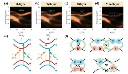
Fig.2.(Color online) (a-d) ARPES spectra of MoSe2 thin layers with different thicknesses[37].(e) Schematic of band structures of MoX2 and WX2 monolayers[40].(f) Classification of excitonic quasiparticles, including neutral excitons (X0), charged excitons (X*), biexcitons (XX), and interlayer excitons (XI).
In addition to X0, there are other types of excitons, such as charged excitons, which are known as trions (X*)[43,44], biexcitons (XX)[43], and interlayer excitons (XI)[15,45,46], as illustrated in Fig.2(f).In the condition of high excitation densities, it is more likely to form XX.Indeed, the XX at 1.585 eV was observed in a freestanding bilayer MoSe2(Figs.3(a) and 3(b)) by regulating three important parameters[47]; more specifically, the integrated intensity of new PL emission peak (XX)as a function of power is superlinear (Fig.3(c)), in which the calculated slopαof XX is 1.23 instead of 2 which can be attributed to the lack of thermal balance between the states.Apart from intralayer excitons in TMDs, interlayer excitons can be formed in homo-bilayers or heterostructures.Different from the interlayer excitons in heterostructures, the interlayer excitons (Fig.3(d)) in homo-bilayers feature larger binding energy and oscillator strength[15].As shown in Fig.3(f),Hornget al.[15]observed that interlayer excitons exist in a bilayer MoSe2at a cryogenic temperature (5 K): from the comparison of measured and simulated reflection contrast spectra for h-BN encapsulated monolayer and bilayer MoSe2(Figs.3(e) and 3(f)), the interlayer exciton resonance appears at 1711 meV between A1sand A2s, which provides new insights in future research in many-body physics.

Fig.3.(Color online) (a) Schematic, optical image, and PL mapping of the freestanding bilayer MoSe2[47].(b) The PL spectra both of the freestanding bilayer MoSe2 and the one on SiO2 substrate, where the "X", "T", and "A" refer to the emission peak of biexcitons, trions, and excitons, respectively[47].(c) The relationship between PL intensities of A and X[47].(d) Illustration of different kinds of excitons in real space[15].(e) Measured and simulated reflection contrast spectra (Rsam/Rsub) of h-BN-encapsulated monolayer MoSe2[15].(f) Measured and simulated reflection contrast spectra of h-BN-encapsulated bilayer MoSe2[15].
2.1.1.Temperature effects
PL spectroscopy serves as a powerful characterization technique to investigate the exciton properties in 2D MoSe2.The excitonic emission behaviors of MoSe2can be modulated by changing the external physical conditions, such as temperature[48,49], substrates[25,50-52], external physical fields[53-58], and so on.
Goddeet al.investigated the effects of temperature on the X0and X*properties in 2D MoSe2by PL spectroscopy[48]:at a cryogenic temperature of 12 K, it is experimentally demonstrated that two distinct PL bands of X0peak at 1.658 eV and X*peak at 1.628 eV, respectively, in which the PL peak intensity of X*peak is significantly greater than that of X0peak due to the presence of carrier doping (Fig.4(a)); the PL intensity of X0increases relative to X*peak with the increase in temperature.Similarly, Rosset al.prepared monolayer MoSe2on the SiO2/Si substrate by the mechanical exfoliation method as presented in Fig.4(b)[57], in which two pronounced PL peaks at 20 K were associated with the higher-energy peak of X0and the lower-energy peak of X*at 1.659 and 1.63 eV,respectively; the X*emission weakened with the temperature increased (Fig.4(c)), in which the thermal fluctuations caused electrons to escape from the bound X*state.Moreover, Shimet al.studied the temperature-dependent PL spectra of monolayer MoSe2(Fig.4(d)) grown by the chemical vapor deposition (CVD) method, where the PL peaks of A and B excitons redshift with the increasing temperature(Fig.4(e))[59].

Fig.4.(Color online) (a) PL spectra of monolayer MoSe2 at different temperatures[48].(b) Two pronounced PL peaks of monolayer MoSe2 at 20 K:the higher-energy X0 and the lower-energy X* at 1.659 and 1.63 eV, respectively.The inset indicates the X* binding energy of approximately 30 meV[57].(c) Temperature-dependent PL spectra of monolayer MoSe2[57].(d) PL spectra of monolayer MoSe2 measured in the temperature range from 0 to 300 K[59].(e) A and B excitonic energies at different temperatures, which were fitted by the Varshni relationships[59].
2.1.2.Substrate effects
The optical properties of TMDs are significantly affected by the substrates due to the changes in the doping levels,dielectric environments, surface impurities, and the radiative decay rates of excitons and trions[25,50-52].Indeed, different excitonic emission behaviors of MoSe2have been observed on diverse substrates[51,52].For instance, Wierzbowskiet al.explored the effects of the dielectric environments on the peak positions and linewidths of excitons in atomically thin MoSe2[51]: in comparison with the X0and X*emission of exfoliated MoSe2layers on the SiO2substrate, the PL peak of MoSe2on h-BN is slightly redshifted and widened; in contrast, the PL peak of MoSe2sandwiched between h-BN exhibits the strongest redshift and the narrowest line width.Moreover, Grzeszczyket al.reported the effects of different substrates on the excitonic properties of MoSe2[52]as follows:the PL spectra on Zr, Mo, Au, and Pt exhibit two well-separated emission peaks dominated by the neutral excitons of X0and the negatively charged excitons of X-; with the increase in the work function of metallic substrates, the relative intensity ratio of X-to X0and the binding energy of X-systematically decrease; for the MoSe2/Pt structure, the PL spectra are dominated by the X0while the PL spectra exhibit two excitonic emission bands of X0and X-when the Fermi level of a metallic substrate is located in the band gap of monolayer MoSe2, i.e.Mo and Au substrates.These findings indicate that monolayer MoSe2can be doped by appropriately selecting the metallic substrates[52].
2.1.3.External field effects
Tuning applied physical fields, such as magnetic and electric fields, provides a promising way for exploring and regulating novel exciton properties of atomically thin MoSe2layers[53-58].For example, by employing an in-plane magnetic field, it is possible to observe dark excitons (Xd) in MoSe2.In 2019, Luet al.utilized high-quality monolayer MoSe2encapsulated in h-BN layers to obtain the excitonic emission with the narrow linewidth at 10 K (Fig.5(a))[55].The Xdin the MoSe2monolayer was measured under the in-plane magnetic field from 0 to 31 T at 10 K where the energy splitting between the bright exciton (Xb) and the higher energy Xdis 1.5 meV (Figs.5(b) and 5(c))[55].Subsequently, Xdwas also observed in a h-BN encapsulated MoSe2monolayer by similar measurements[56], and the splitting energy between the Xband Xdis consistent with the previous report[55].Moreover, the magnetic field dependence of the PL intensity and the four energy dispersions corresponding to different exciton states in Fig.5(d) can be observed, whose energies vary almost linearly at the high magnetic fields within the range of 15-30 T[56].

Fig.5.(Color online) (a) PL and reflectance contrast (RC) spectra of h-BN encapsulated monolayer MoSe2 at 10 K, where the Xb and XT represent the bright neutral excitons and the trions bands, respectively[55].(b) PL intensity map of encapsulated monolayer MoSe2 at different in-plane magnetic fields[55].(c) PL spectra of samples measured at 0 and 31 T[55].(d) Magnetic field dependence of PL intensity map of monolayer MoSe2[56].(e)Gate voltage dependencies of PL intensities for X* and X0, respectively[57].(f) Calculation results of the exciton band structures of bright KK and dark KΛ in the MoSe2 bilayer[54].
On the other hand, the electric field modulation provides a convenient method for the active tunability of excitons in MoSe2layers.Rosset al.investigated the gate voltage dependence of PL spectra in monolayer MoSe2on the 300 nm SiO2/n+-doped Si substrate, demonstrating that the emission behavior of excitons can be regulated by adjusting the gate voltage[57]: as shown in Fig.5(e), the maximum PL intensity of X0is approximately equal to that of the saturated X* when the X0band disappears, indicating that the total amount of X0and X*is conserved in the applied voltage scope and the radiative decay rates of both X0and X*are similar.Consequently, the number of exciton species can be reflected by the PL intensity, and the reversible electrostatic regulation of excitons from the positively charged excitons(X+) to X0and X-can be achieved by utilizing a back-gated FET device embedded with a MoSe2monolayer[57].Recently,Hagelet al.demonstrated the significant effect of electrical field on the interlayer hybridization of R-stacked MoSe2homo-bilayers when applying an out-of-plane electrical field,providing a fascinating insight into the tunability of moiré excitons in MoSe2homo-bilayers[54]: The dark exciton exhibits a significant redshift under an out-of-plane electric field and its PL intensity increases significantly, which can result in the phonon sidebands playing a dominant role in the excitonic emission; the interlayer excitons undergo a strong redshift and their emission dominates PL when the electric field intensity is increased (Fig.5(f)).
2.2.Modification of optical emission through the Purcell effect
In the integrated systems of TMDs and optical microcavities, the excitons in TMDs will interact with the photons in microcavities.In the case of the energy exchange rate or the coupling strength (g) between photons and excitons is less than the decay rate of photons or excitons, which falls into the weak coupling regime[60,61].Theoretically, this regime can be expressed asg≤|γex-γcav|/2,affected by the decay rates of excitons (γex) and cavity photons (γcav)[61].
In the weak-coupling regime, the Purcell effect in the TMD-microcavity system, plays a crucial role in manipulating the spontaneous emission rate of microcavity[40,62], which enables an enormous potential in many applications of vertical-cavity surface-emitting lasers (VCSELs)[63], LEDs[64], and single-photon sources[65,66].In this case, the photons are confined in the optical microcavities, rendering them capable of enhancing the light-matter interactions and further increasing the density of the cavity photonic state.As a result, the excitonic spontaneous emission rate of the radiative recombination in TMDs is significantly accelerated, and the excitonic emission intensity is increased near the cavity resonance energy, resulting in the narrow linewidth and finally leading to the enhancement of the PL intensity at the resonant energy[10,67-70].In general, the Purcell effect can be expressed by the Purcell factor (FP) as below[71]:
According to Eq.(1), the Purcell factor is closely related to the cavity resonance wavelength (λ) and the refractive index (n)of layered materials in cavities, the cavity quality factor (Q),and the mode volume (V).A larger quality factorQoften accompanies less photon loss, while a smaller cavity mode volume indicates a more compact cavity size.Thus, it is crucial for a microcavity to increase theQand reduce theV, which is conducive to the Purcell enhancement.
When a 2D MoSe2layer is coupled to an optical microcavity, the spontaneous emission rate of MoSe2can be tailored by the Purcell effect, especially theVandQparameters of the microcavity[7,26,30,72].In 2019, Lepeshovet al.demonstrated that Mie resonances were achieved by coupling MoSe2to silicon nanowires through the precise optimization of the geometric and material parameters, in which the PL intensity of Xbwas enhanced by two orders of magnitude[72].Subsequently, Zhanget al.positioned monolayer MoSe2into the plasmonic microcavity (Fig.6(a)): The plasmonic gap modes were tuned to overlap with the spectral position of A exciton(Fig.6(b)); furthermore, this plasmonic microcavity possesses a significant binding effect on the electric field (Fig.6(c)),which can be attributed to an extraordinarily small mode volumeV, leading to the PL and Raman intensities of MoSe2being significantly enhanced[26].Apart from 2D MoSe2samples, the Purcell effect was also employed in modifying the spontaneous emission rate of MoSe2-based vdW heterostructures.Fanget al.reported that the h-BN encapsulation of monolayer MoSe2not only narrowed the emission linewidth but also caused a significant effect on the exciton-photon coupling by the Purcell effect[7].Experimentally, encapsulating a MoSe2monolayer in h-BN layers can produce a narrow linewidth PL approaching the uniform exciton linewidth, as shown in Fig.6(e); moreover, the exciton radiative rate in this vdW heterostructure can be regulated by changing the encapsulation layer thickness of h-BN due to the Purcell effect, as presented in Fig.6(f)[7].Alternatively, Parket al.placed the WSe2/MoSe2heterostructure onto the structure of Au nanodisks-PPhC, as illustrated in Fig.6(g)[30]: The PPhC mirror reduces the Purcell factor to about 1.273 × 10⁻²and minimizes the local optical density of the out-of-plane polarization states, resulting in the radiative decay suppression and the increasing radiative lifetime of the interlayer excitons, as demonstrated in Fig.6(h), and the nano-photonic platform was utilized to engineer the radiative decay rate to effectively modulate the exciton lifetime (Fig.6(i)).When the spacing distance is greater or less than the optimal condition spacing, the field absorption in the Au medium is stronger and the coupling with the PPhC mirror is weaker, discouraging the radiative decay suppression[30].
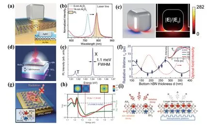
Fig.6.(Color online) (a) Schematic of a monolayer-MoSe2 coupled plasmonic microcavity[26].(b) Simulated scattering spectra of MoSe2 coupled microcavities, where the blue dashed and the red solid lines correspond to the MoSe2 monolayers without/with the Al2O3 coating, respectively.The yellow PL spectrum is from the MoSe2 monolayer on a quartz substrate[26].(c) The distributions of surface charge and electric field[26].(d) Illustration of a MoSe2 monolayer encapsulated by h-BN on SiO2/Si[7].(e) The PL spectrum of MoSe2 encapsulated by h-BN layers exhibits the neutral(X) and the charged (T) exciton bands at 7 K[7].(f) The bottom h-BN thickness dependence of X radiative lifetime of monolayer MoSe2.The red dotted line shows the intensities of the electromagnetic field.The inset presents the normalized time-resolved photoluminescence (TRPL) intensities with different bottom h-BN layers[7].(g) Diagram of the WSe2/MoSe2 heterostructure coupled with Au nanodisks on the PPhC[30].(h) The energy dependences of the averaged Purcell factors of γmean and the coefficients of σ(γ)/γmean, respectively[30].(i) The left panel is the typical interlayer excitons in a heterostructure and the right panel represents long-lived interlayer excitons in a heterostructure coupled with the nano-photonic microcavity[30].
3.Polaritons in MoSe2
3.1.Exciton-polaritons in MoSe2
When the strong coupling between photons and excitons in TMDs is achieved, new quasi-particles with half-light and half-matter properties, known as EPs, can be formed.More specifically, the strong coupling regime can be expressed as below[60]:
where theγexandγcavare the decay rates of excitons and cavity photons, respectively.
As illustrated in Fig.7(a), in the F-P microcavity system with the active media of TMDs, the microcavity has a strong confinement effect on photons, while 2D TMDs provide excitons formed by the pairs of electrons and holes.In this case,the exciton emission is resonant with the resonant photon mode, and the photons are periodically absorbed and emitted at the Rabi frequency of Ω, which is called Rabi oscillation.The Rabi splitting as presented in Fig.7(b) is generated and EPs are formed when the coupling strength is large enough.The basic properties of EPs can be understood through the polariton dispersions, which present two anticrossing branches, including the upper polariton branch(UPB) and the lower polariton branch (LPB).In 1992, Weisbuchet al.observed that the Rabi splitting experimentally and the formation of EP can be attributed to the strong coupling regime of exciton-photon in a semiconductor quantum well microcavity[73], paving the way to study EPs in semiconductor microcavities.After that, many researchers have investigated the phenomena of Rabi splitting in classical semiconductor microcavities and a variety of microcavities have recently provided a rich platform for exploring EPs in TMDs[74-76], as shown in Fig.8.
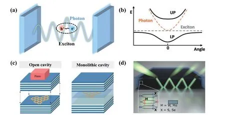
Fig.7.(Color online) (a) Illustration of exciton-photon interaction in the case of an F-P microcavity system.(b) Schematic of angle-resolved optical response in the exciton-photon strong coupling regime, exhibiting the anti-crossing characteristics[77].(c) Structures of monolayer MoSe2 integrating into an open cavity (left) and a monolithic cavity (right), respectively[33].(d) Schematic of the self-hybridized F-P cavity in bulk TMDs[78].
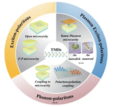
Fig.8.(Color online) Various polaritons are formed in TMDs-coupled cavities, including EPs, PEPs, and phonon-polaritons.
3.1.1.Individual atomically thin MoSe2
In general, the structure of a 2D semiconductor microcavity is mainly composed of the top and bottom mirrors, two dielectric spacer layers, and the active material in the middle region[79].The active layer of MoSe2, according to its structure can be divided into individual MoSe2semiconductor materials, MoSe2-based heterostructures, and the coupling structures consisting of MoSe2and quantum wells.In 2015,Liuet al.reported the first experimental demonstration of EPs-based TMDs[80], which also promotes the research of the novel properties and potential applications of EPs in MoSe2based on microcavity systems (Table 1)[8,23,27,29,33-36,81,82].
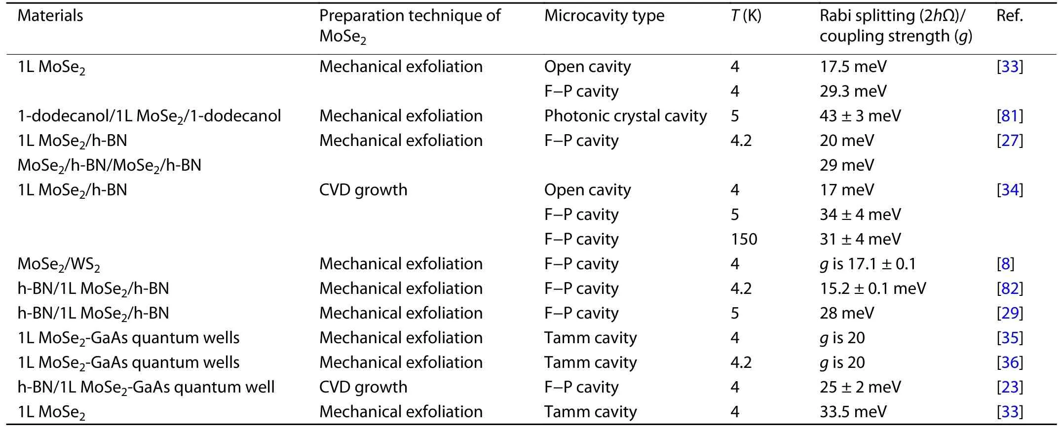
Table 1.Strong coupling regime in atomically thin MoSe2.
Subsequently, Lundtet al.integrated mechanically exfoliated MoSe2monolayer into the open cavity and the monolithic microcavity (Fig.7(c)), to achieve the strong coupling with different Rabi splitting energies and obtain EPs at cryogenic temperatures; with the increasing temperature, the oscillator strength of MoSe2was reduced and the linewidth was increased, whereas the Rabi splitting decreased[33].In addition to the atomically thin MoSe2, the thick layer of MoSe2asillustrated in Fig.7(d) can also be utilized for the low-quality resonators, which is strongly correlated with its high background permittivity[78].In fact, Munkhbat observed the splitting of angle-resolved reflection (ARR) map of mechanically exfoliated thick layers of MoSe2, where the A and B excitons hybridized with the FP modes of MoSe2, resulting in the formation of three EP bands[78].
3.1.2.MoSe2-based heterostructures
2D layered heterostructures constructed by different TMDs take advantage of the vdW forces, which have peculiar physical properties and create an intriguing stage for manipulating the light-matter coupling regime.On the one hand,the h-BN encapsulation of TMDs offers uniform dielectric screening of the coulomb interaction, reduces the spatial heterogeneity of exciton emission, and thus narrows its emission linewidth[83].On the other hand, h-BN can protect the TMD layers in the heterostructures to avoid the damage and contamination caused by the deposition of various dielectric layers in the subsequent preparation of microcavity structures[84].Therefore, the h-BN encapsulation of atomically thin MoSe2is an attractive strategy to control the light-matter coupling in the TMD-microcavity systems.In 2015, Dufferwielet al.coupled the MoSe2/h-BN quantum wells into a tunable microcavity (Fig.9(a))[27]: The strong coupling with anti-crossing behavior due to the interaction between X0and cavity modes was observed in a single MoSe2/hBN with a Rabi splitting of 20 meV (Fig.9(b)), and the Rabi splitting value was increased to 29 meV in a double MoSe2/hBN/MoSe2heterostructures.Subsequently, Gillardet al.placed a large-area MoSe2monolayer encapsulated by h-BN into tunable open microcavity, to achieve strong exciton-photon coupling[34].In detail, the MoSe2monolayer grown on h-BN was embedded in the F-P microcavity (Fig.9(c)), where strong coupling was observed resulting in a Rabi splitting of 34 ± 4 meV at 5 K (Fig.9(d))and 31 ± 4 meV at 150 K[34].Recently, Paiket al.presented a method to obtain the strong coupling regime by the nondestructive integration of the h-BN encapsulated MoSe2into the F-P microcavity (Fig.9(e)) without introducing excessive defects, in which a transferable DBR connected to the substrate by the vdW force was used as the top DBR to form the F-P microcavity with a high-quality factor Q (>2000)(Fig.9(f))[29].Meanwhile, the resonance of the microcavity can be controlled by the thickness of h-BN and the spin-coating speed of polymethyl methacrylate (PMMA)[29].Besides,Zhanget al.integrated a h-BN encapsulated MoSe2/WS2heterostructure with a twisted angle of about 56.5° into the microcavity, resulting in the strong coupling (Fig.9(g)) of the moiré excitons with the cavity photons[8].

Fig.9.(Color online) (a, b) A tunable hemispherical cavity coupled with the MoSe2/hBN heterostructures formed by a planar and a concave DBR and the corresponding strong coupling behavior with a Rabi splitting of 29 meV, respectively[27].(c) Schematic of a MoSe2/h-BN heterostructure embedded in the F-P microcavity[34].(d) Angle-resolved photoluminescence (ARPL) image of a MoSe2/h-BN heterostructure in a monolithic cavity[34].(e) Schematic of a high-quality F-P microcavity device embedded with a h-BN encapsulated monolayer MoSe2[29].(f) Measured and fitted reflection contrast spectra of the bare cavity mode and the one with hBN layers[29].(g) ARR map of a MoSe2/WS2 heterostructure measured at 5 K[8].
3.1.3.Hybrid structures of MoSe2 and quantum wells
Atomically thin MoSe2combined with GaAs quantum wells have been used as active materials for microcavities[23,35], which can generate hybrid states of distinct excitons with the same photon mode.In the strong coupling regime, the hybrid polaritons can provide an attractive technique to combine the advantages of different material systems in the same device[40,85].For example, in the case of a microcavity device embedded with a MoSe2monolayer and four GaAs quantum wells, the microcavity quality factorQcan reach 1095[35](Figs.10(a) and 10(b)), the excitons in these quantum wells are spectrally close to the A exciton resonance of the MoSe2monolayer, achieving the regime of strong coupling (Fig.10(c)) and obtaining the hybrid EP modes composed of excitons in both the dielectric quantum wells and monolayer.Moreover, the addition of the GaAs layer to the heterostructure can enhance the process of polariton-electron scattering and promote the condensation of EPs[23].Experimentally, Anton-Solanaset al.demonstrated the formation of bosonic condensation of EPs at a cryogenic temperature (4 K) by inserting the h-BN encapsulated MoSe2monolayer and quantum wells into the F-P microcavity(Fig.10(d))[23]; in addition, the formation of condensate in lower energy has been demonstrated by the pump power dependent ARPL of such a MoSe2microcavity device(Fig.10 (e)).

Fig.10.(Color online) (a) Schematic of the microcavity device embedded with a MoSe2 monolayer and four GaAs quantum wells[35].(b) The calculated reflectivity spectrum of the Tamm-plasmon microcavity[35].(c) ARPL of the Tamm microcavity of a MoSe2 monolayer at 4 K[35].(d) Illustration of a MoSe2 monolayer encapsulated by h-BN is inserted into an F-P microcavity structure and the optical microscope image of the full device[23].(e) The pump-power dependent polariton dispersions for a MoSe2 microcavity[23].
3.2.Plasmon-exciton polaritons in MoSe2
The combination of the metallic nanostructures with TMDs offers another testbed for the formation of hybrid modes between EPs and plasmons, known as PEPs, in which the surface plasmons formed by metallic nanostructures have the optical confinement of subwavelength mode and are facile to achieve the strong coupling regime.In general, the plasmon-exciton coupling states can also be described by the coupled oscillation model[86].Also, the strong coupling can be expressed as the following condition[87]:
where theΓcavandΓemare the decay rates of plasmonic cavities and emitters, respectively.
Metallic nanostructures can be classified into different configurations, including one-dimensional (1D) and 2D structures, such as metallic nanowires, nanorods, nanodisks,nanosheets, and films, as illustrated in Fig.8.The combination of these metallic nanocavities with TMDs provides a convenient way to dynamically modulate the strongly coupled devices.As a result, the coupling of emitters and nanocavities can enable novel optoelectronic and nano-photonic applications.Previously, silver nanorods[86], gold nanorods[88], and silver nanodisk arrays[89]were successfully demonstrated in the strongly coupled systems with the WSe2, WS2,and MoS2monolayers, respectively.However, the strong coupling between MoSe2and these metallic nanostructures remains to be further explored.To date, the strong coupling systems based on metallic nanostructures and atomically thin MoSe2enable several surface enhancement applications by improving luminescence efficiency[90], Raman emission intensities[26],and nonlinearity characteristics[36].
With the appropriate structural engineering, a microcavity consisting of a DBR mirror and a metal film may form a Tamm-plasmon microcavity, resulting in the unique Tamm plasmon state formed at the interface between the DBR mirror and the metal film, which can significantly reduce the mode volume and increase Rabi splitting energy[35,91].Moreover, different from traditional surface plasmon-polaritons[92],the Tamm plasmon-polaritons can be stimulated directly by the external optical beam[93].Presently, the Tamm plasmon polaritons have been investigated in atomically thin MoSe2.In 2016, Lundtet al.integrated an exfoliated MoSe2monolayer into a Tamm microcavity (Fig.11(a)), in which a strong coupling led to a Rabi splitting of 33.5 meV, and PEPs were formed at a cryogenic temperature of 4 K[33].Subsequently,Wurdacket al.demonstrated that mechanically exfoliated monolayer MoSe2and multiple quantum wells of AlAs/Al0.25Ga0.75As were prepared into a Tamm microcavity, in which the Wannier-type of excitons in GaAs quantum wells,the strongly bound excitons in a monolayer MoSe2and the cavity modes in Tamm structure were strongly coupled to form the hybrid EPs[35].In 2018, Waldherret al.constructed a Tamm microcavity, in which a monolayer MoSe2and four GaAs quantum wells were combined as active layers[36].A strong coupling regime involving Tamm plasmon, and the excitons in GaAs quantum-wells and MoSe2monolayer, were realized in the Tamm microcavity together with the excitondriven bosonic condensation[36].On the other hand, investigation of the excitation-power dependence of the hybrid EPs generated in the microcavity is one of the critical benchmarks for the formation of coherent condensates.Experimentally, the polariton condensation for the hybrid polariton mode in the MoSe2-GaAs microcavity (Fig.11(b)) exhibits the super-linear increase of the emission intensity, the blueshift of the emission energy, and the significant reduction of emission linewidth (Figs.11(c) and 11(d))[36].In addition, monolayer MoSe2was integrated into the Tamm microcavity structure (Fig.11(e)), where the strong coupling was established by the light-matter interactions of the Tamm mode and the trion band of MoSe2(Fig.11(f)), giving rise to the bright luminescence in the ground state of the polariton under the nonresonant light excitation[94].Moreover, strong up-conversion luminescence of resonantly excited polariton states was observed, in which the trion-polariton preserved the valley polarization and opened opportunities for revealing the spin valley physics of polaritons[94].
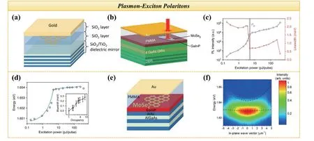
Fig.11.(Color online) (a) Illustration of the structure of a Tamm microcavity[33].(b) A Tamm-plasmon microcavity employs a monolayer MoSe2 and four embedded GaAs quantum wells as active layers[36].(c) Power dependences of PL intensity and linewidth for MoSe2 monolayer, respectively[36].(d) Blueshift of the polariton mode as a function of excitation power[36].(e) Schematic of a MoSe2-integrated Tamm microcavity[94].(f) ARPL map of a Tamm microcavity, in which the UPB and LPB are indicated by black dotted lines[94].
Furthermore, the phonon-polariton can be generated by the strong photon-phonon coupling that generally exists in polar insulators in the spectral range from terahertz to midinfrared frequencies[92,95].In addition, the strong hybridization between plasmons and phonon polaritons can form plasmon-phonon-polaritons[96], enabling mid-infrared photonic applications.As discussed above, diverse strong light-matter coupling strategies have been developed to effectively control light-emitting characteristics of atomically thin MoSe2.
4.Light-emitting devices
4.1.Light-emitting diodes
Benefiting from the unique optical and electrical properties, the emerging TMDs are widely applied in optoelectronic devices, such as LEDs and photodetectors.Different from conventional LEDs, these TMD-based LEDs can be readily integrated into various prevailing substrates[97](e.g.Si, SiO2).The broad emission wavelengths from ultraviolet to mid-infrared regions can be tuned to satisfy a variety of optoelectronic applications.More importantly, the unique valley degree of freedom in direct-gap monolayer MoSe2enables the development of valley-polarized, spin or chiral LEDs or even spin lasers, which can act as a competitive type of circularly polarized light source in spin-optoelectronic and valleytronic applications.The selection of luminescence media is essential to develop high-performance light sources.Among the discovered 2D materials, atomically thin TMDs have sparked many research activities in optoelectronic devices due to their competitive advantages, such as high carrier mobility[98], unique spin-valley coupling[99], and tunable band gap[100].Particularly, some TMDs with direct bandgaps have exhibited significant application prospects for next-generation atomically thin LEDs[101,102].An LED is normally based on spontaneous emission induced by electrical excitation or driving[98], in which the structure is often composed of active media (e.g.p-n junction), electrodes, and optical elements.
In general, electrons bound to the ground state in TMDs can be excited to the higher energy state.Then they will relax to the lower energy state and recombine with the holes in the ground state, leading to emitting photons.Before the recombination process, relaxation and Coulomb screening often result in a reduction in the emitted photon energy[98].In the PL of monolayer TMDs, the exciton emission often plays a key role in the relaxation of excited states.Moreover,the type-Ⅱ band alignment in the heterostructures can effectively promote the charge transfer for carriers and the formation of a high built-in potential[9].Such a type-Ⅱ alignment causes the electrons and holes of excitons localized in individual layers to form interlayer excitons, which may have longer lifetimes than the ones of intralayer excitons[98].In a MoSe2/WSe2heterostructure (Fig.12(a)), the interlayer-exciton lifetime of 1.8 ns was measured by time-resolved PL,which was at least one order of magnitude longer than the one of intralayer exciton[18].Furthermore, such interlayer excitons have the permanent out-of-plane dipole moment and the distinctive optical selection rule[16], which are in favor of fabricating efficient optoelectronic devices[17].By regulating the vertical gate voltage and the excitation power, the tuning of interlayer exciton energy and the energy of the PL band can be realized, respectively[18], indicating that the heterostructure constructed by monolayer TMDs is a promising structure to expand their optoelectronic applications[18].For example, electrical contacts at different layers in the MoSe2/WSe2heterostructures with twisted angles of 0° and 60° can form atomically thin p-n diodes with optional emission between the opposite spin and polarization characteristics[16], where the interlayer tunneling current across the interfaces of heterostructures generate singlet and triplet excitonic emission components.The emission behaviors of singlet and triplet interlayer excitons can be further controlled by electrostatic doping, excitation power, and injection current.
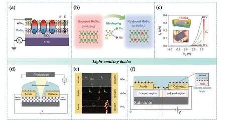
Fig.12.(Color online) (a) The structure of MoSe2/WSe2 heterostructure device[18].(b) Illustration of Nb-doping mechanism[19].(c) The rectifying behavior of p-n diode based on MoSe2[19].(d) The formation process of a p-i-n junction[3].(e) Light-emitting zones of WSe2, MoSe2 and WS2 devices, respectively[3].(f) Illustration of a two-terminal LED[3].
Besides, the p-n homojunction constructed by TMDs is another structure for the light source.The typical MoSe2shows the characteristics of an n-type semiconductor, while the intrinsic n-type MoSe2can be transformed into a p-type semiconductor by elemental doping[19].Jinet al.synthesized such an n-type MoSe2and a p-type MoSe2by Nb-doping(Fig.12(b)), which were employed to construct a p-n diode with ideal electrical characteristics (Fig.12(c))[19].What is more, the diodes based on the p-type/intrinsic/n-type(p-i-n) homojunction have an intrinsic region, which makes them different from p-n diodes and suitable for low-power high-speed applications[103].Ouet al.designed a device realizing the ion redistribution process, which leads to spontaneous injection and accumulation of carriers to form the dynamic p-i-n junction (Fig.12(d))[3].The CVD-grown monolayers of WSe2, WS2, and MoSe2were employed to construct a two-terminal light-emitting device, where WSe2exhibited the hole-transport behavior[104], MoSe2presented the balanced ambipolar transport properties[105], and WS2presents an n-type character due to the presence of sulfur vacancies[3,106].The electroluminescence exhibits a strong dependence on the spatial location (Fig.12(e)) and the p-i-n junction enabled the control of the light-emitting regions in these devices (Fig.12(f)), in which a dynamic shift of the light-emitting zone was found due to the increase of the voltage, paving the way for developing the dynamic LEDs based on TMDs monolayers[3].
4.2.Single-photon emitters
Single-photon emitters (SPEs), as the key building blocks for quantum technologies, can be easily integrated with nano-photonic devices[107].As a consequence, SPEs have advantages for extensive applications in the fields of quantum computing[108], quantum information processing[109]metrology, etc.An ideal SPE emits only one photon at a time to a spatiotemporal mode, different from the cases of coherent photons[109].
Solid-state SPEs, including semiconductor quantum dots(QDs)[110]and color centers in wide band gap materials such as diamond nanocrystals[111], are particularly interesting since they can be monolithically integrated with photonic crystals,microcavity structures, or waveguides.Recently, stable and bright SPEs have been found in both individual TMDs[112-114]and heterostructures[115].2D characteristics of TMDs provide high flexibility for engineering and integration, which presents itself as an ideal platform for the creation, localization, and regulation of SPEs, such as integrating into photonic structures by mechanical strain or heterostructure stacking[116].Structural defects in TMDs can often act as effective carrier trapping centers, and their isolated centers often serve as efficient SPEs[117].As an example, both WSe2monolayers[112,118]and WSe2-based heterostructures[119]have QDlike defects, which exhibit a series of localized PL peaks with narrow linewidths of 100 to 150μeV and their emission intensities can reach hundreds of times stronger than the excitonic emission case.
For mechanically exfoliated samples, such QD-like defects typically appear at the cracks or edges of the samples, mainly due to the local strain caused by the process of exfoliation or transferring[120].However, for the CVD-grown samples, the formation of these defects can be attributed to the presence of impurities[109].In mechanically exfoliated MoSe2monolayer (Fig.13(a)), Brannyet al.observed the narrow QD-like and discrete PL peaks at 4 K (Fig.13(b)), originating from spatially isolated regions caused by the unintentionally local strain, in which the performance of single-photon emitters was tuned by utilizing the magnetic field(Fig.13(c))[21].Likewise, the narrow PL lines of localized exciton emission were observed at 4 K in the exfoliated monolayer MoSe2, in which the Zeeman effect with an excitongfactor of about 4 was revealed by magneto-optical PL measurements[120].In practice, quantum emitters can be obtained by deliberately creating local strain regions to form potential traps.Yuet al.generated the local strain by depositing monolayer MoSe2on protrusions with different diameters (250,120, and 50 nm) located on the substrate by the CVD method(Fig.13(d)); more specifically, the unstrained zones of the monolayer MoSe2only produced an emission tail with both weak and broad features, while for the case of 50 nm trap,the linewidth of the antibunching exciton peak decreased significantly (Fig.13(e))[20].Beyond individual MoSe2, MoSe2-based heterostructures have also emerged as attractive candidates in the study of atomically thin SPEs.For example, quantum light emission of Moiré-confined interlayer excitons(Fig.13(f)) was successfully demonstrated with the photon antibunching feature (i.e.the hallmark of quantum light) in a MoSe2/WSe2heterostructure with a stacking angle of about 60°[121].
4.3.Coherent-light sources
In general, a laser consists of the gain medium, resonators, and pumping or excitation sources.TMD monolayers possess intrinsic merits such as strong exciton emission,direct bandgap, atomically flat, and easy integration, which are regarded as born successors for developing 2D semiconductor lasers[22].The system composed of TMDs and microcavity is an attractive device structure for on-chip CLSs, whose coherent emission can be derived from the processes of conventional photon lasing, polariton lasing, and Bose-Einstein condensation (BEC)[79].Therein, the polariton lasers are the superior on-chip CLS and the input energy thresholds may be reduced by several orders of magnitude compared with the ones of conventional photon lasers[122,123].Until now, numerous studies have demonstrated the formation of EPs by embedding monolayer MoSe2in optical cavity systems, such as F-P microcavities[27,33], DBR open microcavities[34], and DBR-metal Tamm cavities[35,36].
VCSEL is a laser with the output lasing emission in a direction perpendicular to the substrate surface, which is an excellent on-chip CLS.The DBRs or metallic mirrors are often employed to realize the microcavity with strong optical confinement and high reflectivity[63].In 2017, a WS2-based VCSEL was demonstrated at room temperature under 532 nm continuous-wave laser excitation, where the VCSEL consisted of a 12.5-pair bottom DBR and an 8.5-pair top DBR[63].According to the dependent relationships between PL emission intensity and excitation power, the working stages can be divided into three regions as below: the spontaneous emission region presents a sublinear correlation due to the quenching of exciton emission caused by non-radiative decay processes;the amplification region exhibits super-linear characteristics;the lasing region presents a linear increase in intensity under the excitation power of 10-100 nW, stable linewidth, and peak position[63].
Currently, the laser devices based on prevailing TMDs mainly use the emission of excitons, and most of the emitted lights are located in the visible and near-IR range.Furthermore, the construction of heterostructures provides more diverse approaches to modify their band gaps, in which interlayer excitons exhibit exceptionally intriguing optical properties beyond the ones of intralayer excitons in monolayers.In some cases, the lifetime of interlayer excitons is much longer than that of intralayer excitons and their PL intensity is much stronger than the intralayer excitons, where interlayer excitons may be employed to realize the BEC and lasing[6].Photon lasing emission based on the interlayer excitons of WSe2/MoSe2heterostructures in type-Ⅱ band alignment was realized by integration into the silicon-nitride grating cavity (Fig.14(a))[22].The WSe2/MoSe2heterostructure with the type-Ⅱ band alignment can form a three-level system (Fig.14(b)), which not only reduces the band gap and easily realizes the population inversion, but also avoids the rapid intralayer radiative loss[22]; compared with excitons in monolayer TMDs, the existence of interlayer excitons in this heterostructure has the tunable long-range dipole interaction and strong valley polarization, greatly enriching the study of multi-body physics.More specifically, as the excitation-dependent photon occupancy ofIp(k≈ 0) reached 1, a transition from linear to super-linear was observed as the increase in the pump power and the linewidth decreased sharply around the threshold (Fig.14(c)), indicating the increase of temporal coherence[22].
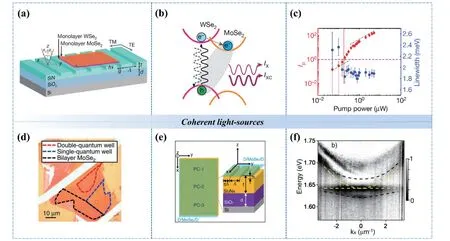
Fig.14.(Color online) (a) Schematic of a WSe2/MoSe2 heterostructure on the silicon-nitride grating cavity system[22].(b) Band alignment of a WSe2/MoSe2 heterostructure[22].(c) The pump power dependences of photon occupancy (Ip) and linewidth[22].(d) Optical image of the MoSe2/h-BN quantum wells[27].(e) Illustration of a monolayer MoSe2 integrated with the photonic crystal microcavity[81].(f) ARR of Dodecanol/MoSe2/Dodecanol-PC on the device with the detuning value of 0.1 ± 0.2 meV approximately[81].
By use of the half-light and half-matter nature of EPs,polariton lasers are not only expected to be a kind of non-classical CLS with significantly low thresholds but also a peculiar device platform for studying multi-body physics and cavity quantum electrodynamics[123].Dufferwielet al.integrated the MoSe2/h-BN quantum wells (Fig.14(d)) into a tunable DBR microcavity[27]: the anti-crossing behavior between exciton and cavity photon dispersion was observed in PL and reflection measurements to prove the strong exciton-photon coupling mechanism in the MoSe2heterostructure, which laid a foundation for developing tunable polariton lasers based on the vdW heterostructure.Nevertheless, the small size or the non-uniform optical quality of TMD monolayers limits the development of polariton lasers.Recently, Liet al.demonstrated a technique, i.e.the combination of 1-dodecanol encapsulation and gold-tape-assisted exfoliation methods[81], in which monolayer MoSe2with high quality at the scale of millimeter to centimeter was prepared with the spatially uniform exciton energy, linewidth and quantum yield.More importantly, the strong coupling (Fig.14(f)) was observed via integrating the macroscopic-scale monolayer into the photonic crystal microcavity (Fig.14(e)), which paved the way for further development of polariton lasers based on TMDs[81].
5.Summary and outlook
In conclusion, we review the development of light-emitting devices based on atomically thin MoSe2.Monolayer MoSe2is a direct bandgap semiconductor, enabling highly efficient optical transitions in the near-IR range.Together with the considerable oscillator strength and the high exciton binding energy, these MoSe2layers are appealing to develop micro light-emitting devices, such as LEDs, SPEs, and polariton lasers.The exciton emission behavior of MoSe2can be modulated by external physical conditions, such as temperature, substrates, and applied physical fields.Both neutral and charged excitons with intriguing characteristics have been researched in depth; moreover, the interlayer excitons of MoSe2-based heterostructures have extended the research frontier.For instance, the intrinsic interlayer excitons between neutral excitons of A and B in the bilayer and fewlayer MoSe2need to be further investigated, which is conducive to the light-emission physics of interlayer excitons and provoke spin-valley related light-emitting applications.
For developing MoSe2-based light-emitting devices, several challenges remain.First of all, the luminescence quantum efficiencies of exfoliated and grown MoSe2layers remain relatively low, preventing their light-emitting applications.To improve the optical quality of MoSe2, the coupled systems composed of MoSe2and various nanocavity structures, such as plasmonic metallic nanostructures and PPhC, provide an alternative strategy to address this difficulty, in which the Purcell effect can be used to reduce the PL linewidth and enhance the quantum efficiency effectively.Moreover, chemical treatment is also an effective method to improve the luminescence of MoSe2.It is also worth stabilizing the quantum efficiency of MoSe2at a high level for a long time by the chemical treatment, which will be highly demanded in practical light-emitting applications.
Furthermore, the MoSe2-based LEDs exhibit promises for industrial applications, such as infrared remote sensing systems[124], photovoltaic fields[125], and night vision systems.Compared with conventional GaAs-based LEDs, the electroluminescence emission peak of monolayer MoSe2is narrower[124], indicating a better wavelength selectivity.Also,this kind of MoSe2-based infrared LEDs with ultrathin architectures have the potential to be used in flexible and/or transparent optoelectronics for wearable displays and health monitors.In addition, the wafer-scale of MoSe2prepared by CVD may be further integrated into the functional device arrays for practical infrared light-emitting applications such as remote controllers, infrared cameras, automated card readers,and infrared light therapy.
Secondly, for polariton lasers, the low value of Q and Rabi splitting energy limits the implementation of strong coupling in MoSe2-embedded microcavity systems and greatly hinders the formation of polariton lasing.Previous polariton lasers based on 2D MoSe2were realized at low temperatures[27,81], while the ability to achieve room-temperature polariton lasing of MoSe2is essential to realistic light-emitting applications.Moreover, by contrast with optical pumping, the electrical pumping of MoSe2is a more practical and feasible method.The investigation of MoSe2polariton lasers by electrical pumping will open up new opportunities for applications of 2D infrared on-chip lasers.Furthermore, it will be appealing to develop valley-polarized polariton lasers, polariton transistors, and polariton logic gates, as well as the integration of polaritonic circuits based on these MoSe2layers.
In brief, atomically thin MoSe2layers, as the crucial building blocks of emerging TMDs, are of significant importance to developing 2D light-emitting devices, while their intrinsic exciton natures need to be further explored.The realization of higher density integration, higher performance, and other features of low-threshold lasers still needs continuous efforts.Last but not least, further development of light-emitting devices and polariton lasers, might flourish applications of the next generation optical interconnection, quantum computing, and quantum information processing.
Acknowledgements
This work is supported by the National Natural Science Foundation of China (No.61904151), the National Key Research and Development Program of China (No.2021YFA1200803), and the Joint Research Funds of the Department of Science & Technology of Shaanxi Province and Northwestern Polytechnical University (No.2020GXLH-Z-020).
杂志排行
Journal of Semiconductors的其它文章
- Chemical vapor deposition for perovskite solar cells and modules
- Highlights in recent wireless power IC research
- Recent advancements in continuously scalable conversion-ratio switched-capacitor converter
- Towards efficient generative AI and beyond-AI computing:New trends on ISSCC 2024 machine learning accelerators
- Millimeter-wave PA design techniques in ISSCC 2024
- Anomalous bond lengthening in compressed magnetic doped semiconductor Ba(Zn0.95Mn0.05)2As2
