Chemical vapor deposition for perovskite solar cells and modules
2024-04-23ZhihaoTaoYuxuanSongBaochangWangGuoqingTongandLimingDing
Zhihao Tao, Yuxuan Song, Baochang Wang, Guoqing Tong,†, and Liming Ding
1School of Materials Science and Engineering, Hefei University of Technology, Hefei 230009, China
2Center for Excellence in Nanoscience (CAS), Key Laboratory of Nanosystem and Hierarchical Fabrication (CAS), National Center for Nanoscience and Technology, Beijing 100190, China
Metal halide perovskites are promising materials for solar cells because of high power conversion efficiency (PCE), tunable bandgap, high defect tolerance, long carrier diffusion length, and low-cost fabrication[1-7].The PCE for perovskite solar cells (PSCs) reaches 26.14% for single-junction cells,29.1% for perovskite/perovskite tandem cells and 33.9% for perovskite/silicon tandem cells, being comparable to that for silicon and other thin-film solar cells[8-10].Perovskite solar cells have been made by solution methods including spin-coating, blade coating and printing[11,12].Alternatively, vapor depositions featuring “gas-gas” or “gas-solid” chemical reaction include co-evaporation, sequential evaporation, and chemical vapor deposition (CVD), needing less or no solvent for device fabrication[13-16].The co-evaporation and sequential evaporation methods are usually performed under high vacuum for the deposition of perovskite films.By contrast, CVD method is normally operated under low vacuum[17,18], which not only eliminates the influence of solvent and external environment, but also reduces the cost, offering an efficiency of 21.98% (Fig.1).

Fig.1.(Color online) Advances of CVD-made PSCs in lab scale.
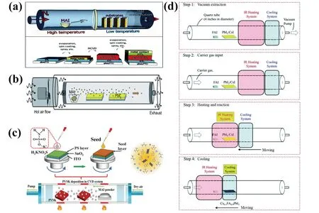
CVD fabrication includes lead halide deposition (PbX2,X = I, Br, Cl) and organic halide deposition (i.e., MAI, FAI)(Fig.2)[19-22].In 2014, Qiet al.used CVD to prepare MAPbI3-xClxfilms, in which PbCl2layer was first deposited in vacuum chamber, followed by MAI evaporation in doublezone furnace with a low pressure of 100 Pa[23].The devices delivered a PCE of 11.8% with long-term storage stability over 1100 h.Later, Luoet al.developed a low-pressure CVD method to make MAPbI3films, in which spin-coated PbI2films and MAI powders were placed in separated zones in furnace under low pressure[24].The as-prepared MAPbI3films were annealed in a humid environment (RH ~60%) and the resultant devices gave a PCE of 12.73%.CVD method not only greatly improves device stability, but also significantly eliminates humidity influence to deposition.Yinet al.proposed a vapor-assisted crystallization for making MAPbI3films, and the devices gave an efficiency over 18%[20].Tonget al.developed a vapor doping technique in combination with vacuum evaporation and CVD to make perovskite films with gradient bandgap, in which CsBr was introduced into perovskite films to obtain Cs0.15FA0.85PbI2.85Br0.15films.The devices gave a PCE of 18.22% with long-term stability[25].CVD technique also shows potential in making perovskite solar modules (PSMs).The fast chemical reaction of conventional solution methods and handling issues make its application more challenging in manufacturing PSMs.In contrast, CVD creates uniform pressures for organic halide (i.e., MAI and FAI) evaporation and mild molecular diffusion of organic halides vapor, enabling to achieve uniform large-area perovskite films and high reproducibility[26].Qiu, Jiang, Qi, and coworkers developed hybrid CVD for scalable fabrication of Cs-FA based perovskite solar modules with sizes of 12,22.8, and 91.8 cm2(PCEs of 14.7%, 12.03%, and 9.34%), respectively (Figs.3(a)-3(c))[27-29].

Fig.2.(Color online) (a) All vapor based CVD.Reproduced with permission[23], Copyright 2014, the Royal Society of Chemistry.(b) Hot air flow assisted CVD.Reproduced with permission[20], Copyright 2016, the Royal Society of Chemistry.(c) Seed-assisted CVD.Reproduced with permission[21], Copyright 2023, Wiley-VCH.(d) Rapid CVD.Reproduced with permission[22], Copyright 2020, the Royal Society of Chemistry.

Fig.3.(Color online) (a) 5 × 5 cm2 PSM made by CVD.Reproduced with permission[28], Copyright 2019, Wiley-VCH.(b) 10 × 10 cm2 PSM made by CVD.Reproduced with permission[27], Copyright 2019, the Royal Society of Chemistry.(c) 5 × 5 cm2 PSM made by rapid CVD.Reproduced with permission[22], Copyright 2020, the Royal Society of Chemistry.
Though promising for PSCs fabrication, the efficiency for CVD-made PSCs and PSMs still lags far behind solution-processed devices because of the residue PbI2, oxygen vacancy defects and high energy barrier from PbI2to perovskite phase[30].CVD technique can be regarded as a two-step deposition, in which the initial PbI2layer is expected to react with organic halide vapor to form perovskite films.The volume expansion from lead halide to perovskite phase impedes organic halide vapor to penetrate into bottom lead halide layer, resulting in large amounts of unreacted lead halide[31].The residue lead halide in devices will act as defects, which not only deteriorate device performance, but also accelerate the degradation of perovskite films and devices[32].To address these issues, Tonget al.introduced NH4Cl into PbI2layer at the first step to form PbI2adduct, which can greatly low the phase transition energy barrier, promoting the complete phase conversion of PbI2to MAPbI3perovskite phase[33].The oxygen defects originated from the oxygen loss in the process of CVD[34].For conventional CVD-made PSCs,the device configuration is mainly n-i-p structure, in which TiO2and SnO2are used as electron-transport layer (ETL).The low pressure and continuous pumping during film formation will inevitably cause the oxygen loss, which creates more defects at ETL/perovskite interface, leading to more carrier recombination[21,27,35].Qiuet al.used C60as the buffer layer to modify SnO2surface, mitigating the surface defects in PSCs and PSMs[27,35].Similarly, Tonget al.introduced potassium sulfamate (H2KNO3S) as the bridge between ETL and perovskite film, which can not only greatly reduce the defects at SnO2/perovskite interface, but also passivate the uncoordinated Pb2+in perovskite, favoring carrier extraction and increasing photocurrent[21].Tong and coworkers developed the intermediate phase and seed assisted growth strategy to control perovskite crystal growth and reduce the energy barrier, yielding a record efficiency of 21.98% for the cells,16.16% for 5 × 5 cm2module and 12.12% for 10 × 10 cm2module, respectively[21].The devices showed T80lifetime over 4000 h for unencapsulated devices under one sun.
In short, CVD method features uniform film, less solvent,low cost, and scalable fabrication.The efficiency for CVDmade devices needs improvement.More research on phase transition, film growth and interface defects are required.
Acknowledgments
We thank the Key Research and Development Project of Anhui Province (2023t07020005), Natural Science Foundation of Anhui Province (2308085QE137), and Anhui Innovation & Entrepreneurship Support Plan for Returned Overseas Students (2022LCX018).L.Ding thanks the National Key Research and Development Program of China(2022YFB3803300, 2023YFE0116800), and Beijing Natural Science Foundation (IS23037).
杂志排行
Journal of Semiconductors的其它文章
- Highlights in recent wireless power IC research
- Recent advancements in continuously scalable conversion-ratio switched-capacitor converter
- Towards efficient generative AI and beyond-AI computing:New trends on ISSCC 2024 machine learning accelerators
- Millimeter-wave PA design techniques in ISSCC 2024
- Light-emitting devices based on atomically thin MoSe2
- Anomalous bond lengthening in compressed magnetic doped semiconductor Ba(Zn0.95Mn0.05)2As2
