Surface Metallization of Glass Fiber (GF) /Polyetheretherketone (PEEK) Composite with Cu Coatings Deposited by Magnetron Sputtering and Electroplating
2024-04-10ZHONGLiJINFanyaCHUPaulTONGHonghuiDANMin
ZHONG Li, JIN Fanya*, CHU Paul K, TONG Honghui, DAN Min
(1.Southwest Institute of Physics, Chengdu 610000, China; 2.City University of Hong Kong, Tat Chee Avenue, Kowloon, Hong Kong 999077, China)
Abstract: Surface metallization of glass fiber (GF) / polyetheretherketone (PEEK)[GF/PEEK] is conducted by coating copper using electroplating and magnetron sputtering and the properties are determined by X-ray diffraction (XRD), scanning electron microscopy (SEM), and electron backscatter diffraction (EBSD).The coating bonding strength is assessed by pull-out tests and scribing in accordance with GB/T 9286-1998.The results show that the Cu coating with a thickness of 30 µm deposited on GF/PEEK by magnetron sputtering has lower roughness, finer grain size, higher crystallinity, as well as better macroscopic compressive stress,bonding strength, and electrical conductivity than the Cu coating deposited by electroplating.
Key words: surface metallization; Cu coating; magnetron sputtering; electroplating
1 Introduction
Polyetheretherketone (PEEK), a high-density thermoplastic polymer with a linear aromatic semicrystalline structure that has exceptional physical and chemical properties as regards toughness, hardness and elasticity, has a wide variety of applications in the aerospace, energy, automotive, and medical industry[1-6].PEEK is often reinforced with glass fibers(GF)[7,8], carbon fibers (CF)[9,10], polytetrafluoroethylene(PTFE) fibers[11], and whiskers[12-16]and among them,glass fiber reinforced polyetheretherketone (GF/PEEK)is a promising composite due to the high temperature resistance, wear resistance, and corrosion resistance as well as excellent mechanical properties.
One of the current trends in engineering structural plastics is to replace traditional metals with GF/PEEK or a mixture of GF/PEEK and alloys to balance the weight and mechanical properties of the overall structure.Without changing the basic properties of the materials, the surface of the composite materials often needs to be metallized to address specific needs such as electromagnetic shielding, filtering, and resistance to thermal radiation.The common metallization techniques include wet dip coating and dry coating,among which electroplating is the most mature technology boasting advantages including the low cost, efficiency, simplicity, and convenience.In fact,electroplating has become an indispensable technology for the manufacturing of electronic components, as it enables the construction of copper circuits and interconnections between layers and implementing superfill without porosity[17-19].Huaet al[20]have prepared a uniform and firm Ni layer on the surface of carbon fibers by electroplating and R Akolkaret al[21]have produced a complex nanopatterned Cu film without pores on porous SiO2by electroplating for precise multilayer interconnects on integrated circuits.Yeet al[22]have prepared nanocrystalline NiW alloy by electroplating and investigated the nucleation and growth process.However, electroplating has drawbacks such as the low yield, poor precision, and not environmentally friendly and there is an industrial need to replace it with cleaner coating techniques.
Magnetron sputtering is an environmentally friendly coating technique offering advantages such as flexible processing, high precision, and good controllability and is widely used in the industry[23-25].SM Changet al[26]and YF Lanet al[27]have synthesized indium tin oxide (ITO) coatings with high visible light transmittance and resistance on polyethersulfone and polyethylene terephthalate substrates by pulsed DC magnetron sputtering and thermal ion-enhanced DC sputtering.X Taoet al[28]have deposited island-like Bi-Te coatings with high Seebeck coefficients on acrylate substrates by DC magnetron sputtering at room temperature and the materials show thermoelectric characteristics.Linet al[29]and Kimet al[30]have prepared flexible circuit boards with copper coatings on polyimide produced by sputter coating.
In this work, electroplating and magnetron sputtering are compared as metallization techniques for GF/PEEK.The microscopic states and macroscopic performance of the two Cu coatings are analyzed systematically in order to identify the best coating technique.
2 Experimental
2.1 Coating preparation
The GF/PEEK composite made of 30% glass fibers (GF) and PEEK was cleaned ultrasonically with acetone and anhydrous ethanol and dried.Owing to the high chemical inertness and low affinity with metals, there are difficulties such as interface mismatch and weak bonding of dissimilar materials when surface metallization is carried out.Therefore, a Hall ion source was used to generate a high-energy ion beam to improve the surface activity of the substrate.Electroplating and magnetron sputtering were performed to deposit the Cu coatings and in order to improve the bonding strength between the metal film and polymer substrate, a 0.35 μm thick Ti interlayer was deposited by magnetron sputtering.A 0.5 μm thick Cu film was deposited plating (sample S1-EP) as a seed layer by magnetron sputtering coating technique, prior to electroplating (sample S1-EP) in 10% sulfuric acid for 10 seconds for activation and then at a current of 0.5 A for 30 min.DC magnetron sputtering was conducted directly on the Cu-coated Ti transition layer (sample S2-MS) for 9 hours at a working air pressure of 0.8 Pa and target current of 3 A.The thicknesses of the Cu coatings on both samples was 30 μm.
2.2 Characterization
The JSM7500F cold field emission highresolution scanning electron microscope (SEM) was used to observe the microstructure of the coatings and X-ray energy spectrometry (EDS) was performed to determine the composition.A Bruker Dimension Icon atomic force microscope equipped with a scanning airair probe made in Germany was employed to examine the three-dimensional morphology in an area of 10 μm ×10 μm.An Oxford NordlysMax3 electron backscatter diffraction tester (EBSD) from Oxford, UK, was used to determine the grain orientation in the coatings.The bonding strength between the Cu coating and substrate was characterized quantitatively by the pull-out test and qualitatively by the scribing method according to GB/T 9286-1998.
3 Results and discussion
3.1 Microstructure and composition
Fig.1 and Fig.2 show the microstructure and composition of the two Cu coatings (S1-EP and S2-MS)and Fig.3 and Table 1 present the three-dimensional morphology and roughness.The surface of S1-EP is dense and flat with spherical particles of φ0.02-0.1 μm densely distributed on the surface and a large gap of about 0.6 μm among particles.S2-MS consists of clusters with a larger size between φ0.6 μm and φ1.0 μm and they are densely stacked forming a uniform and regular polyhedral shape with a very narrow gap of about 0.25 μm between each other.The morphology depends on nucleation and growth of the two coatings.The residence time of deposited atoms on the substrate and migration rate during the residence time has an important influence on nucleation and growth.Due to the low ambient temperature during electroplating, the deposited atoms obtain little adsorption energy through thermal upheaval, thereby reducing the frequency of vibration along the vertical direction, which resulting in a longer residence time on the substrate.That is,the efficiency of electroplating is high.During the residence time, the atoms migrate randomly on the surface of the substrate and as the coating process proceeds, the atoms on the substrate increase, diffuse,coalesce, and nucleate.The migration rate is limited by the low frequency of the deposited atoms vibrating along the horizontal direction and so the binding probability of the nuclei and other diffused atomsis low, leading to a small overall nucleation density.However, it is different in magnetron sputtering during which the deposited atoms have a high kinetic energy[31]and reach the substrate to quickly transfer excess energy.Energy dissipation raises the local temperature[32], giving rise to a higher migration rate of the deposited atoms and increasing the nucleation probability and nucleation density.
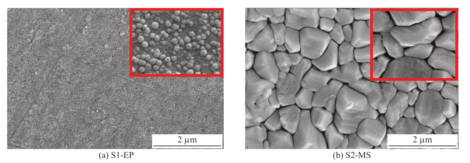
Fig.1 Microstructure of the electroplated Cu coating and the magnetron sputtered Cu coating
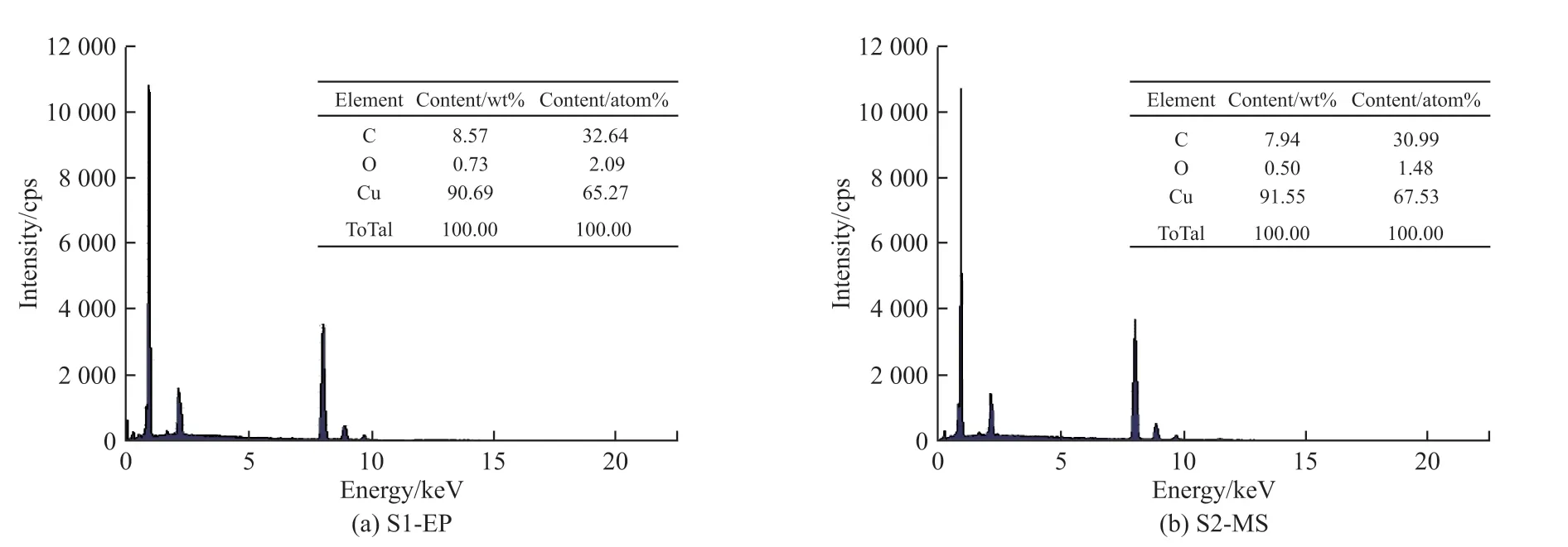
Fig.2 Composition of the electroplated Cu coating and the magnetron sputtered Cu coating

Fig.3 Surface morphology of the electroplated Cu coating and the magnetron sputtered Cu coating
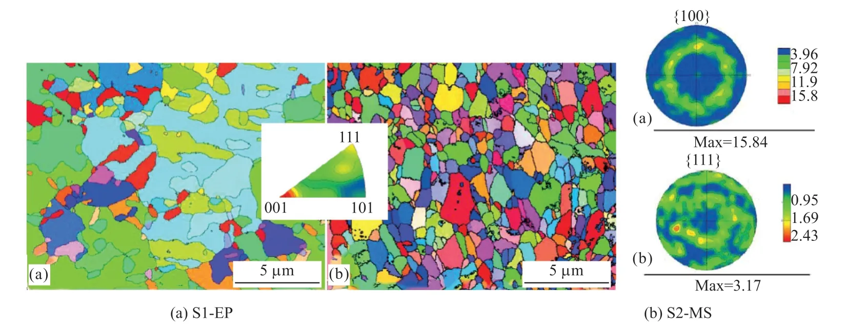
Fig.4 Orientations and polar diagram of the electroplated Cu coating and the magnetron sputtered Cu coating

Fig.5 Recrystallization images of the electroplated Cu coating and the magnetron sputtered Cu coating

Table 1 Roughness of the electroplated Cu coating and the magnetron sputtered Cu coating
The elemental composition of S1-EP and S2-MS is about the same and the Cu contents are 90.69%and 91.55%, respectively which is relatively high in purity.The remaining elements are C and O elements,8.57% and 0.93% in S1-EP and 7.94% and 0.50% in S2-MS, respectively.C and O in S1-EP come from the brightener, complexing agent, retarder, and other solvents in the electroplating solution, whereas C and O in S2-MS come from the substrate and contamination in the vacuum chamber.
Comparing the surface morphology of the Cu coatings, S1-EP is less dense and flat with a roughness of 53.63 nm, whereas S2-MS shows a value of 20.13 nm which is about half of the former.During electroplating, because of low temperature and energy of copper ions, the residence time of copper ions on the substrate surface is longer.More atoms arriving later are captured for more extensive nucleation[31], resulting in larger, less dense, and more widely spaced nucleation centers in the early stage of film formation.In contrast,the nucleation sites in the magnetron-sputtered film are smaller but more numerous and dense.
3.2 Grain orientation
Figs.4 and 5 show the grain orientation, polar maps and recrystallization images by EBSD of S1-EP and S2-MS, respectively.The polar map of S1-EP shows a strong {100} weave, but S2-MS does not exhibit a pronounced weave.There is a high occupancy of {111} fiber weave instead.There are fewer recrystallized grains in the electroplated coatings of less than 40% of the overall area, while there is a higher degree of recrystallization in the magnetron sputtered film of over 70% of the overall area.
Fig.6 shows the fraction of area occupied by different grain sizes in S1-EP and S2-MS.The size of the grains in these two coatings differs greatly,with the grains in the magnetron sputtering film being finer and more uniform and grains smaller than 0.1 μm accounting for 55.52% of the total area and the rest of the grains randomly distributed from 0.10 to 1.95 μm.The grain size and size distribution of the electroplated film are greater, with grains smaller than 0.5 μm accounting for 30.19% and grains smaller than 0.9 μm grains accounting for 64.62%.The remaining grains are randomly distributed in the range from 0.95 to 16.75 μm.
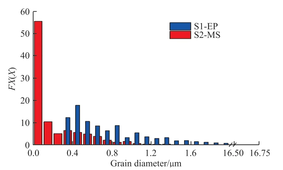
Fig.6 Grains size of the electroplated Cu coating and the magnetron sputtered Cu coating
Generally, the surface energy varies from one crystalline surface to another and the {111} plane has the lowest surface energy.The {111} fiber weave in the film makes it easy to relax the stress by plastic deformation in the direction of the film surface under stress but offers high resistance to deformation in the vertical direction of the film.The presence of a strong{111} fiber weave in the film is helpful in overcoming the negative effects of the “e-wind” effect[33]to improve the electrical conductivity of the film.Therefore, the deposited conductive Cu coatings have a high amount of the {111} fiber structure.
The optimal distribution of grain orientation is related to the growth rate of the crystals during nucleation and film formation, temperature and thermal fluctuation, as well as difference in the thermal conductivity between different crystallographic orientations.Grain orientation is highly susceptible to electroplating environmental conditions because the growth rate is extremely fast.The low dislocation energy of Cu crystals is further reduced by the small amount of impurity elements in the environment and impurities in the electroplating solution can also change the grain orientation.This is why the direction of the lower crystalline surface changes to that parallel to the deposited surface along {100} despite the {111} and{110} fibrous structures produced by electroplating.In contrast, due to the higher temperature and thermal fluctuation during magnetron sputtering, grains prefer to grow in the direction of higher thermal conductivity,i e, {111} crystal direction.Due to continuous bombardment by high-energy particles in magnetron sputtering, the kinetic energy and heat exchange render the high energy state unstable.Some of the grains recrystallize spontaneously by the high energy changing from a high energy state to a more stable low energy state.During this process, because of the large number of grain boundaries in the magnetron-sputtered Cu film, the nucleation rate of recrystallization is high.However, at the same time, the grains in the magnetronsputtered film do not become too large as the result of a lower rate of grain boundary migration caused by the lower coating temperature, although more pronounced recrystallization occurs as shown in Fig.5[33].
It is generally accepted that the finer the metal grains (shown by S2-MS), the more grains with different orientations and the longer the grain boundaries.Grain boundaries accentuate slip and fracture and the larger the proportion of grain boundaries, the greater the resistance to dislocation and the stronger the resistance to deformation.If the metal has a coarser grain size such as that shown by S1-EP, the anisotropy and inhomogeneity of grains increase, leading to increased notch sensitivity and reduced impact toughness to negatively impact the serviceability.
3.3 Phase structure
X-ray diffraction is used to analyze the phase structure of S1-EP and S2-MS and the results are shown in Fig.7.The peak angle, height, area, and halfheight width of the characteristic peaks are calculated by Jade software, as shown in Table 2.Both S1-EP and S2-MS exhibit selective growth along Cu(111).The characteristic peaks of S2-MS are sharper and narrower,whereas those of S1-EP are broader.The peak height of the characteristic peak of Cu(111) in the electroplated film is only 74% of that of Cu (111) in the magnetronsputtered film, indicating that the crystallinity of the magnetron-sputtered film is better.It results from the solute in the electroplating solution.In addition to the main salt in the electroplating solution, there must be additional salts, complexing agents, buffers, anode activators, additives, and other solutes and they play a role in the conductive flow of mutual replacement or as a third solute in the gap causing lattice distortion.

Fig.7 XRD spectra of the electroplated Cu coating and the magnetron sputtered Cu coating
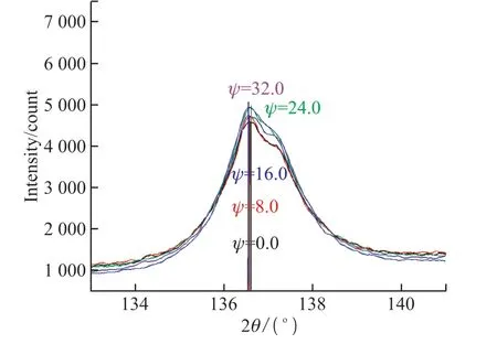
Fig.8 Diffraction pattern and 2θ-sin 2Ψ relationship for different angles of incidence (S1-EP)
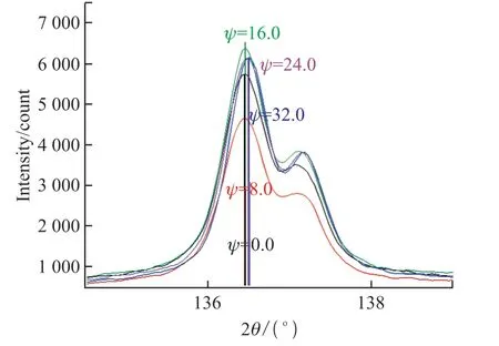
Fig.9 Diffraction pattern and 2θ-sin 2Ψ relationship for different angles of incidence (S2-MS)

Table 2 XRD parameters of the electroplated Cu coating and the magnetron sputtered Cu coating
3.4 Residual stress
In addition to the roughness ,orientation, grain size and crystallinity, the macroscopic residual stress is another crucial factor influencing the properties.Even if the stress does not destroy the film, it can impact the structure and properties of the film such as adhesion strength, defects, as well as electrical, superconducting,and magnetic properties[34].In order to analyze the macroscopic stress in the coatings, calculation and analysis of the internal stress are conducted by X-ray and electron diffraction as shown in Figs.8 and 9.
X-rays are used to irradiate the substrate to reflect the macroscopic stresses in coatings in terms of grain spacing.In the presence of residual stress,as the incident angle changes, the crystal lattice and interplanar crystal spacing change to promote the Bragg diffraction peak change that is related to the stress.According to this principle, the specimen is linked to the detector with theθ-2θrelationship.The fixedΨmethod is adopted to measure the peaks at 0°, 8°, 16°,24° and 32° to obtain the slopeMof the line 2θ-sin 2Ψand then calculate the stressδaccording to Eq.(1).
The slopeMof the 2θ-sin 2Ψrelationship is negative for both S1-EP and S2-MS, indicating that the residual stress is compressive.The stress is 15.63 MPa in the electroplated film and 86.02 MPa in magnetronsputtered film.
The residual compressive stress arises from a combination of factors mostly caused by thermal fluctuation during crystallization and nucleation, plastic deformation caused by high-velocity impact of Cu ions on the surface of the materials, and chemical or physical changes transmitted from the surface to the substrate.All the Cu ions undergo the process of nucleation,nucleation growth, and complete crystallization after deposition on the substrate captured by the surface energy of the substrate.During nucleation, the energy of the micro regions on the surface of the substrate fluctuates and changes under constant bombardment by Cu ions, which becomes the source of the nucleation and supplies additional surface energy for nucleation.As deposition continues, new nuclei are formed by diffusion and migration of atoms and new grains appear and agglomerate to form clusters.
In this process, the grain boundaries become the place where the elastic distortion energy and chemical interaction energy accumulate and it is why they are always in a higher energy state compared to the inner grains.Eventually the accumulated grain boundary energy becomes part of the residual internal stress.Due to the difference in surface electron density and thermal expansion coefficient between the coatings and substrate, residual thermal stress is generated during deposition.Cu ions lead to heat transfer during deposition and as a result, the surface temperature of the substrate rises.What’s more, the rise in temperature leads to transformation of chemical bonds in the film.This is why the residual stress in the magnetronsputtered coating is higher than that in the electroplated coatings.
Normally residual stress is detrimental to coatings and industrial components.Excessive or uneven residual stress may lead to deformation, cracking, or even destruction but tensile and compressive stress are different in nature.It is believed that the residual tensile stress determines the contraction force of the film, which can easily cause stress corrosion, film peeling,etc.The residual compressive stress determines the expansion force of the film and causes blistering when the expansion force is greater than the bonding force.However, in the allowable stress range, a certain degree of compressive residual stress can improve the fatigue strength and corrosion resistance and therefore,it is beneficial to the performance of coatings and structural materials because of the ability to inhibit expansion of cracks.The magnetron-sputtered film with a higher compressive stress exhibits better resistance to crack extension when subjected to loads.
3.5 Bonding strength
The bonding strength between the Cu coatings and substrate is characterized quantitatively by the pull-out test and qualitatively by the scribing method according to GB/T 9286-1998[35]and the results are presented in Table 3.Both S1-EP and S2-MS are judged to be grade 0 because the two coatings stay intact, with completely smooth cut edges and no signs of dislodgement after the scribing test.The pulling test is carried out by welding the copper wire to the metal film and applying a vertical load to the wire for pulling.The load is increased gradually until the film base separates and the critical load at which the film layer fails is determined as the bonding strength of the film base.The bonding strength of the film base is 0.2 MPa for S1-EP and 1.6 MPa for S2-MS.In other words, the bonding strength of the magnetron-sputtered film is significantly better.

Table 3 Bonding strength of the electroplated Cu coating and the magnetron sputtered Cu coating
During the bonding test, micro-cracks appear between the film and substrate at the place where stress concentrations such as interface pores, microgrooves and grain boundaries, and the micro-cracks expand and extend rapidly until the film is separated from the substrate.There are three reasons why the magnetronsputtered film has higher bond strength.First of all, the finer the copper grains in the film, the larger the total area of the grain boundaries.Extension of micro-cracks from the interface to the grain boundaries is hindered and the direction of extension is deflected resulting in more deformation energy dissipation, thereby improving the fracture resistance.the grains in S2-MS are much finer than those in S1-EP , and fine grain can help to relieve stress and improve the bonding strength of coatings.Secondly, as shown in Fig.4, the magnetron-sputtered coating has a larger percentage of{111} fiber weave in the coating, thus making it easier for the film to deform plastically in the direction of the film surface under stress, consequently relaxing the stress caused by the load and increasing the resistance to deformation in the vertical direction[33].Thirdly,during the crack extension phase in the film, if there is a higher residual compressive stress, the compressive stress can form a compressive stress zone at the end of the crack tip as a complete ligament to hinder the extension of surface cracks through the bridging effects of the micro-zone pressure field.It can increase the toughness of the coating and improve the critical failure strength of the film to extend the lifetime of the film.The compressive stress in S2-MS is much higher than in S1-EP and the compressive stress is much more pronounced and effective in hindering crack extension,thereby leading to higher bonding strength between the film and substrate.
3.6 Electrical resistance
The sheet resistance of S1-EP and S2-MS is determined by double electrical measurement combined with the four-point probe.During the test,the probe is connected to the tester through four probes and the conductive film.The two probes on the outer end generate the current field and the two probes on the inner end measure the potential and calculate the resistance of the film according to Ampere’s law.The results are shown in Table 4.The sheet resistance of S1-EP is 3.33 Ω/□, and 2.00 Ω/□ of S2-MS and it is evident that the conductivity of the magnetronsputtered film is significantly better.

Table 4 Sheet resistance of the electroplated Cu coating and the magnetron sputtered Cu coating
The roughness and porosity of the electroplated film is greater than that of the magnetron-sputtered film.The rough surface fills the microscopic valleys and pores with more insulating air and reduces the actual contact area between the probe and film, resulting in higher resistance.Theoretically, the grain boundary has a hindering effect on the directional movement of electrons and this effect is related to the orientation of the grain boundary.The larger the orientation difference of the grains on both sides of the grain boundary, the stronger the hindering effect[33,36].As shown by the orientation imaging of S1-EP and S2-MS(Fig.4), although the grains in the magnetron-sputtered film are finer and there are more grain boundaries, the range of the grain dislocation angle is distinctly smaller and more evenly distributed, with about 35% of small angle grain boundaries and 65% of large angle grain boundaries.The orientation difference between the grains on both sides of the grain boundaries is smaller,thus leading to less obstruction to electrons.However,there is a wide range of dislocation angles of the grains in the electroplated film, of which more than 85% are large-angle grain boundaries and the small-angle grain boundaries are further reduced, so that the orientation difference of the grains in the electroplated film is larger and the hindrance to electrons is significantly stronger.In addition, the magnetron-sputtered Cu coating has a bigger percentage of {111} fibee weave,which is very helpful in overcoming the negative effects of the “electron wind” effect[33]to improve the conductivity.
4 Conclusions
Electroplating and magnetron sputtering are used to deposit thin complete and dense Cu coating on the GF/PEEK composite.The Cu coating prepared by magnetron sputtering has a cleaner and flatter microstructure, finer grains, better crystallization,and more {111} fiber weave.In terms of the macroscopic performance, the residual stress in both the electroplated and magnetron sputtered Cu coatings is compressive with 15.63 MPa for the electroplated film and 86.02 MPa for the magnetron-sputtered film.The bonding strength of the magnetron-sputtered film is higher at 1.6 MPa compared to 0.2 MPa of the electroplated Cu film.The electroplated Cu coating has a higher sheet resistance of 3.33 mΩ/□ and that of the magnetron-sputtered coating is only 2.00 mΩ/□.Although magnetron sputtering coatings are much more expensive than electroplating, the conductive copper coatings deposited on GF/PEEK composites offer significantly better performance.
Conflict of interest
All authors declare that there are no competing interests.
杂志排行
Journal of Wuhan University of Technology(Materials Science Edition)的其它文章
- Effect of VEGF/GREDVY Modified Surface on Vascular Cells Behavior
- Evolution of Biofilm and Its Effect on Microstructure of Mortar Surfaces in Simulated Seawater
- Synthesis of Organic-Inorganic Hybrid Aluminum Hypophosphite Microspheres Flame Retardant and Its Flame Retardant Research on Thermoplastic Polyurethane
- Effect of Size Change on Mechanical Properties ofMonolayer Arsenene
- Effects of Sinusoidal Vibration of Crystallization Roller on Composite Microstructure of Ti/Al Laminated Composites by Twin-Roll Casting
- LPCS Ni-Zn-Al2 O3Intermediate Layer Enhanced SPS NiCr-Cr3C2Coating with Higher Corrosion and Wear Resistances
