Effects of vacancy and external electric field on the electronic properties of the MoSi2N4/graphene heterostructure
2024-03-25QianLiang梁前XiangyanLuo罗祥燕GuolinQian钱国林YuanfanWang王远帆YongchaoLiang梁永超andQuanXie谢泉
Qian Liang(梁前), Xiangyan Luo(罗祥燕), Guolin Qian(钱国林),Yuanfan Wang(王远帆), Yongchao Liang(梁永超), and Quan Xie(谢泉)
College of Big Data and Information Engineering,Institute of New Optoelectronic Materials and Technology,Guizhou University,Guiyang 550025,China
Keywords: MoSi2N4,vacancy defects,external electric field,Schottky contacts
1.Introduction
In recent years, 2D materials have received much scientific attention due to their novel electronic transport, piezoelectric, optical and mechanical properties.[1-5]Among all 2D materials, graphene (Gr),[6,7]hexagonal boron nitride (h-BN),[8-10]phosphorene,[11,12]arsenene[13,14]and transitionmetal dichalcogenides (TMDs)[15-17]are the most important and widely researched.MoS2[18,19]is a typical representative of TMDs, which is extensively used as a channel material in transistors with promising application prospects.In particular,MoS2has great potential for applications in photocatalysis,[20]Li-ion batteries,[21]field-effect transistors (FETs),[22]energy storage,[23]sensors,[24]etc.Subsequently, the emergence of 2D van der Waals (vdW) heterostructures stacked by two 2D materials has surprised researchers with some unanticipated results.For instance, Zhanget al.[25]proved that MoS2/g-C3N4heterojunction enhances the hole separation and transfer ability of photogenerated electrons by broadening the spectral absorption range,showing excellent photocatalytic performance.Huanget al.[26]successfully synthesized a MoS2/Gr heterostructure using the facile hydrothermal method, and they found that the MoS2/Gr heterostructure exhibits preferable photo-response activity under the irradiation of sunlight.Mikhalevaet al.[27]reported that the combination of VS2monolayer with Gr has good lithium capacity, remarkable electronic conductance and high sorption/desorption rates,making it a promising anode material for Li-ion batteries.Neupaneet al.[28,29]investigated the Gr/MoS2heterostructure systematically using first-principles calculation.They found that non-magnetic Gr/MoS2heterostructure changes to magnetic material as a result of Mo site vacancy defects.Furthermore, the C vacancy defect also makes the original nonmagnetic water-adsorbed Gr/MoS2heterostructure into a magnetic system and the spins of electrons in 2s and 2p orbitals of C atoms give the principal effect of magnetism in wateradsorbed Gr/MoS2heterostructure materials with C sites vacancy defects.
More recently, two new layered 2D materials, MoSi2N4(MSN) and WSi2N4(WSN), were successfully synthesized by Honget al.,[30]who used the chemical vapor deposition(CVD)method.They also predicted an emergingMA2Z4family by first-principles calculation,whereMis a transition metal(Mo,W,V,Nb,Ta,Ti,Zr,Hf or Cr),Ais Si or Ge,andZdenotes N, P or As.Luet al.[31]found that 2D MSN modified with 3d transition-metal (TM) atoms can be an effective alternative to noble metal-based catalysts for energy conversion and storage.By constructing a novel Janus MoSH/MSN heterostructure, Nguyenet al.[32]found that vertical strain and electric field can achieve n-p type Schottky contact transitions and even ohmic contacts.Xiaoet al.[33]systematically investigated the catalytic activity of TM atoms and non-metal atom-doped MSN monolayer for hydrogen evolution reaction(HER), and they found that the O, P, Fe and Nb atom-doped systems can be selected as promising HER electrocatalysts with relatively good structural stability.
The electronic properties of 2D vdW heterostructures are sensitive to doping, adsorption, vacancy defect, biaxial strain and external electric field.In this contribution,we construct an MSN/Gr heterostructure and investigate the effects of vacancy and external electric field on the electronic properties of the MSN/Gr heterostructure based on density functional theory(DFT).First, we compare the band structure of the MSN/Gr heterostructure with the band structures of MSN and Gr, and find that it is a simple superposition of two monolayers.The calculated binding energy is-0.69 eV,and the negative binding energy proves that the MSN/Gr heterostructure we have built is stable.Then, we investigate the effect of vacancy defects on the magnetic properties,work function,charge transfer at the interface and electrostatic potential of MSN monolayer or MSN/Gr heterostructure, respectively.Finally, we study the modulation effect of the external electric field on the MSN/Gr heterostructure.
2.Method
First-principles calculations were performed to obtain the electronic properties of the intrinsic MSN/Gr heterostructure and its defective structures using the Viennaab initiosimulation package (VASP)[34,35]based on DFT.The exchangecorrelation potential between the interacted electrons was described by the generalized gradient approximation (GGA)with the Perdew-Burke-Ernzerhof(PBE)[36]functional.The projected augmented wave(PAW)potential[37]was used to describe the interactions between ionic cores and valence electrons.The plane-wave kinetic cutoff energy was set to be 500 eV and the reciprocal space was sampled with a 9×9×1 Monkhorst-Pack mesh grid.The convergence criteria for energy and force were set to be 1×10⁻⁶eV and 0.01 eV/°A,respectively.A vacuum layer of 15 °A was applied to avoid the interaction between adjacent periodic slabs.Moreover,the DFT-D3 method proposed by Grimme[38]was considered to correct the effect of vdW interaction.The Grimme DFT-D3 method is widely used and is thought to better describe the weak vdW interactions between the monolayer MSN and Gr than the DFT-D2 method.Instead of using a semi-empirical dispersion-correlated as in DFT-D2,the dispersion coefficients are now computedab initioby time-dependent DFT employing known recursion relations for the higher-multipole terms.
3.Results and discussion
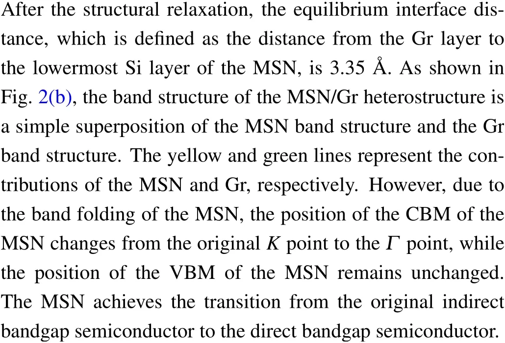
3.1.Electronic properties of the MSN and MSN/Gr heterostructure without defects
The optimized lattice constants of the MSN and Gr are 2.91 °A and 2.46 °A,respectively,which are in good agreement with other works.[39-41]As can be seen from the top views of the MSN and Gr (as shown in Fig.1(a) and 1(c)), MSN and Gr are both composed of hexatomic rings.From the side views,the MSN is built by an N-Si-N-Mo-N-Si-N septupleatomic layer and the Gr is built by a single-atomic layer.Figures 1(b)and 1(d)show the band structures of the monolayer MSN and Gr,and the Fermi level is set to zero.The calculated value of the band gap of the MSN is 1.80 eV,which is slightly smaller than the experimental results(1.94 eV),[30]but agrees with the results calculated by other researchers.[42]The conduction band minimum (CBM) and valence band maximum(VBM) of the MSN are located at the high-symmetryKandΓpoints in the Brillouin zone, respectively.The CBM and VBM are located at different high-symmetry points in the Brillouin zone,so the MSN is an indirect band gap semiconductor.However,the calculated value of the band gap of the Gr is approximately equal to zero with the Fermi level just passing through the Dirac point.The Dirac cone of the Gr is located at the high-symmetryKpoint.The energy and momentum of the electrons both have a linear dispersion relationship,which makes the effective mass of Gr relativistic electrons approximately equal to zero.

Fig.1.The side and top views of(a)MSN and(c)Gr;band structures of(b)MSN and(d)Gr.The Fermi level is set to zero.
The cohesive energy(Ecoh)is firstly considered to assess the possibility of experimentally synthesizing the MSN
whereEtot,EMo,ESiandENare the energy of the MSN supercell and the ground state total energy of a single Mo,Si and N atom,respectively.Thenrepresents the cell expansion multiplier of the MSN supercell.In our calculation,the value ofnis equal to 1.The calculated cohesive energy is-8.44 eV/atom,indicating the possibility of experimentally synthesizing the MSN structure.

Then,we plot the plane-averaged differential charge density along theZ-plane in Fig.2(c) to investigate the charge transfer properties at the interface of the MSN/Gr heterostructure.The plane-averaged differential charge density (Δρ) is defined as follows:
whereρvdW,ρMSNandρGrare the plane-averaged charge densities of the MSN/ Gr with or without defects, the isolated MSN single layer and the isolated Gr layer.The pink and blue areas represent the accumulation and depletion of the charges,respectively.We find charge transfer behavior at the interface of the MSN/Gr heterostructure.In addition, the charges are accumulated in the MSN layer and depleted in the Gr layer,implying that the charges are transferred from the Gr layer to the MSN layer.Due to the charge transfer behavior at the interface, a built-in electric field is generated at the interface pointing from the Gr layer to the MSN layer.
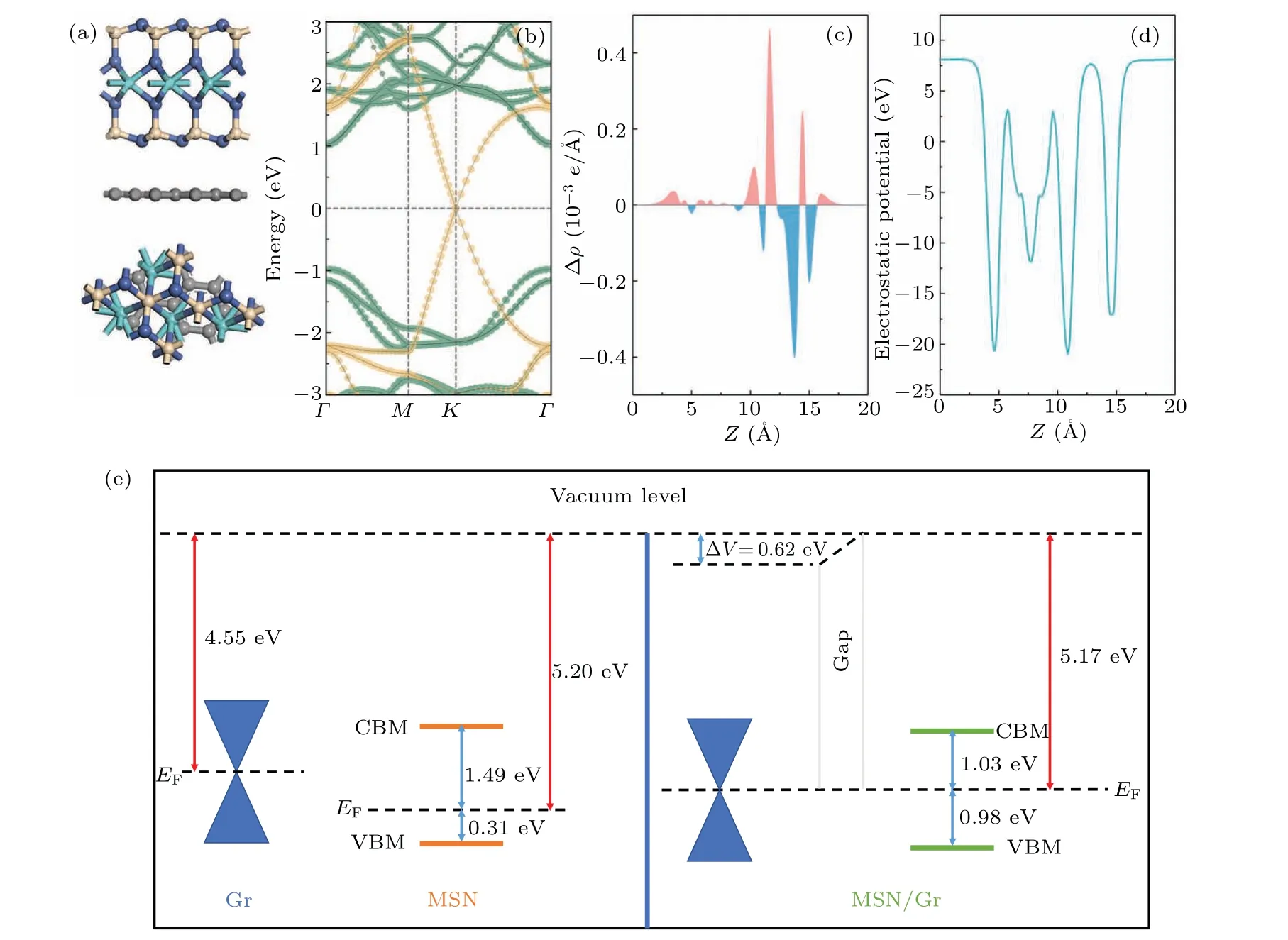
Fig.2.(a) The side and top views of the MSN/Gr heterostructure.(b) The projected band structure of the MSN/Gr heterostructure.The Fermi level is set to zero and the yellow and green lines represent the contributions of the MSN and Gr,respectively.(c)The plane-averaged differential charge density between two interfaces along the Z-plane of the MSN/Gr heterostructure.The pink and blue areas represent the accumulation and depletion of the charges,respectively.(d)The effective electrostatic potential of the MSN/Gr heterostructure.(e)The band alignments of the Gr and MSN before(left)and after(right)formation of the heterostructure. EF is the Fermi energy level.
Figure 2(d) shows the effective electrostatic potential of the MSN/Gr heterostructure.When the MSN/Gr heterostructure is completely relaxed,the effective electrostatic potential of the MSN layer is deeper than that of the Gr layer, indicating the existence of a strong electrostatic field between the two layers.The effective electrostatic potential in the MSN layer part shows a symmetrical property due to the symmetry of the MSN structure.The significant potential drop between the MSN and Gr leads to the generation of a built-in electric field at the interface of the MSN/Gr heterostructure.The band alignments of the Gr and MSN before and after the formation of the heterostructure are depicted in Fig.2(e).We calculate the work functionWMof the MSN and Gr, which can be defined as the difference between the vacuum energy level and the Fermi energy level
whereEvacuumandEFare the energy of the vacuum energy level and the Fermi energy level,respectively.The calculated work functionWMof the MSN is 5.20 eV, which is greater than 4.55 eV of the Gr, as shown in Fig.2(e).The charge transfer from the layer with a small work function(Gr)to the layer with a large work function(MSN)is attributed to the disparity in the work functions between these two layers.As the amount of charge transfer increases,the Fermi energy levels of the Gr and MSN keep decreasing and increasing,respectively,and eventually both reach the same energy level.It is worth noting that the work function of the MSN/Gr heterostructure(5.17 eV) lies just between the work functions of the Gr and MSN,implying that charges are accumulated in the MSN layer and depleted in the Gr layer.This is also consistent with previous conclusions on the plane-averaged differential charge density.
3.2.Electronic properties of the MSN and MSN/Gr heterostructure with defects
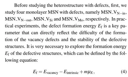
whereEvacancyandEintrinsicare the energy of the MSN(MSN/Gr) with and without defects, whilemis the number of the removedXatoms andµXis the chemical potential of the removedXatom.The chemical potentials of the removed Si, Mo and N atoms are energy of per atom of their corresponding stable structures.For the removed Si and Mo atoms,the reference phases used are their bulk structures.For the removed N atom, the reference phase used is its stable N2molecule in the gas phase.The positive(negative)value of the formation energy denotes the non-spontaneous(spontaneous)process.The values of the calculated formation energyEfare listed in Table 1.All obtained values of the formation energy for the four defective structures are negative, implying that the four defective structures are stable in the air.Among them,the MSN VSimodel has the smallest value of the formation energy (-10.02 eV) and the MSN VN-inmodel has the largest value of the formation energy(-3.76 eV).Our results demonstrate that the MSN VSiis the most stable model and the MSN VN-inis the most unstable one.
Figures 3(a)-3(d) show the side views of the pristine MSN with vacancies and the positions of the defective atoms are circled in red.In our calculations, spin polarization was considered.The band structures of the monolayer MSN with vacancies are shown in Figs.3(e)-4(h).It is noteworthy that when four different vacancy defects are introduced, defective energy levels are generated near the Fermi energy level in both the up and down spin channels.It can also be easily seen that the band structures of both the MSN VN-outand the MSN VMomodels show perfect symmetry in both the up and down spin channels, indicating that N-out and Mo vacancies cannot introduce magnetism into the pristine MSN.However, when N-in and Si vacancies are introduced, the up and down spin channels show asymmetry,suggesting that the MSN VN-inand MSNVSimodels are magnetic systems with magnetic moments of 0.809µB/cell and 1.966µB/cell,respectively.
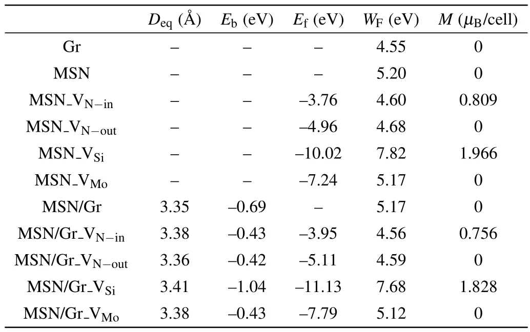
Table 1.Calculated equilibrium interface distance(Deq),binding energy(Eb),formation energy(Ef),work function(WF)and total magnetic moment(M).
When N-in vacancy is introduced,the Fermi energy level passes through the defective energy level in the up-spin channel.While in the down-spin channel, there is no overlap between the Fermi energy level and the energy band, so the MSN VN-inmodel is a half-metal.In contrast,the MSNVMomodel is still a semiconductor.Unlike both the MSNVN-inand MSN VMomodels,the MSN VN-outand MSNVSimodels exhibit metallicity.Furthermore,the work functions of four defective monolayers are also calculated in our work.Our calculation shows that the work function of the pristine MSN decreases when N and Mo vacancies are introduced and increases when Si vacancy is introduced.
We then use four defective monolayers to match Gr to form MSN/Gr heterostructure with vacancies,namely, MSN/GrVN-in, MSN/Gr VN-out, MSN/GrVSiand MSN/GrVMo, respectively.As listed in Table 1, the obtained equilibrium interface distances of the four defective heterostructures are 3.38 A°, 3.36 A°, 3.41 A° and 3.38 A°, respectively,which are quite close to the distance of the pristine MSN/Gr heterostructure and are all larger than the pristine MSN/Gr heterostructure.
The binding energy(Eb)can be used to describe the stability of the MSN/Gr heterostructure with and without defects
whereEvdW,EGrandEMSNare the energy of the MSN/Gr heterostructure with and without defects, the energy of the isolated Gr and MSN, respectively.A smaller value of the binding energyEbindicates a more stable heterostructure.For the pristine MSN/Gr heterostructure, the calculated binding energyEbis-0.69 eV, indicating that the pristine MSN/Gr heterostructure is a stable structure.The values of the binding energy of the MSN/Gr VN-in, MSN/GrVN-outand MSN/GrVMomodels are extremely close to each other

Fig.3.The side views of the intrinsic MSN with vacancies: (a)MSN VN-in,(b)MSN VN-out,(c)MSN VSi and(d)MSNVMo.Band structures of the monolayer MSN with vacancies: (e)MSNVN-in,(f)MSN VN-out,(g)MSN VSi and(h)MSN VMo.Fermi level is set to zero.

Fig.4.The side views of the MSN/Gr heterostructure with vacancies:(a)MSN/Gr VN-in,(b)MSN/Gr VN-out,(c)MSN/Gr VSi and(d)MSN/GrVMo.The projected band structures of the MSN/Gr heterostructure with vacancies: (e) MSN/GrVN-in, (f) MSN/Gr VN-out, (g) MSN/GrVSi and(h)MSN/GrVMo.The Fermi level is set to zero and the yellow and green lines represent the contributions of MSN and Gr,respectively.
Figures 4(a)-4(d)show the side views of the MSN/Gr heterostructure with vacancies and the positions of the defective atoms are circled in red.Figures 4(e)-4(h) correspond to the projected band structures after the introduction of N-in,N-out,Si and Mo vacancy defects, respectively.Just like the monolayer MSN with vacancies,the up and down spin channels of N-out and Mo vacancy defects are symmetrical and neither system is magnetic.In contrast, the up and down spin channels of N-in and Si vacancy defects are asymmetrical and both are magnetic systems with magnetic moments of 0.756µB/cell and 1.828µB/cell, respectively.We also fnid that the band structure of the defective heterostructure is just a simple superposition of its corresponding defective monolayer MSN and Gr band structures.
Furthermore,in order to investigate the specifci origin of magnetism, the magnetic moments contributed by the atomic orbitals of C, N, Si, Mo atoms of four magnetic models(MSN VN-in, MSN VSi, MSN/Gr VN-inand MSN/GrVSi)are listed in Table 2.For the MSNVN-inmodel, the magnetic moments contributed by 2s and 2p atomic orbitals of N atoms are 0.000µB/cell and 0.072µB/cell, respectively.The magnetic moments contributed by 3s and 3p atomic orbitals of Si atoms are both-0.00µB/cell and the magnetic moments contributed by 4p, 4d and 5s atomic orbitals of Mo atoms are 0.020µB/cell, 0.711µB/cell and 0.008µB/cell, respectively.The total magnetic moment of the MSN VN-inmodel is 0.809µB/cell, which is mainly contributed by the 2p atomic orbitals of N atoms and the 4d atomic orbitals of Mo atoms.For the MSN VSimodel, the total magnetic moment is 1.966µB/cell and it is mainly contributed by the 2s and 2p atomic orbitals of N atoms.For the MSN/Gr VN-inand MSN/Gr VSimodels, the total magnetic moments are 0.756µB/cell and 1.828µB/cell, respectively.The magnetic moments of the MSN/Gr VN-inand MSN/GrVSimodels contributed by atomic orbitals of C atoms are both zero,indicating that vacancies do not affect the magnetic properties of the underlying Gr but only the upper MSN.Like the MSNVN-inmodel, for the MSN/Gr VN-inmodel, the 2p atomic orbitals of N atoms and the 4d atomic orbitals of Mo atoms are the main cause of the magnetism.Like the MSN VSimodel, for the MSN/Gr VSimodel,the magnetic moment is mainly contributed by the 2s and 2p atomic orbitals of N atoms.
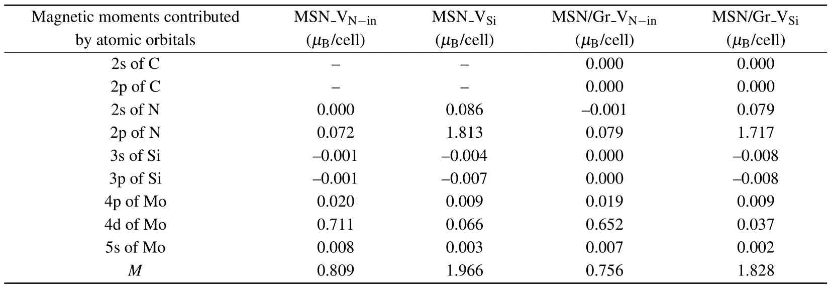
Table 2.Magnetic moments contributed by atomic orbitals of C,N,Si and Mo atoms and total magnetic moment(M).

Fig.5.The plane-averaged differential charge densities between two interfaces along the Z-plane of the MSN/Gr heterostructure with vacancies:(a)MSN/Gr VN-in,(b)MSN/Gr VN-out,(c)MSN/GrVSi and(d)MSN/GrVMo.The pink and blue areas represent the accumulation and depletion of the charge,respectively.
We then plot the plane-averaged differential charge densities to investigate the charge transfer difference between the pristine and defective MSN/Gr heterostructures in Figs.5(a)-5(d).After comparison, it is clear that charge transfer at the interface decreases after the introduction of N-in and Si vacancy defects and increases after the introduction of N-out and Mo vacancy defects.However, the charges at the interface are still depleted at the Gr layer and accumulated at the MSN layer.The direction of the built-in electric field does not change with the generation of vacancies.Obviously, N-out and Mo vacancy defects have little effect on charge transfer at the non-interfaces.While N-in and Si vacancy defects have a large effect on the charge transfer near the positions of the corresponding defective atoms.
Figures 6(a)-6(d) show the effective electrostatic potentials of the MSN/Gr heterostructure with vacancies, respectively.The introduction of Si vacancy defect creates an energy difference(ΔΦ1)of 3.46 eV in the vacuum region between the two sides, while the remaining three defects do not create an energy difference in the vacuum region.Four vacancy defects break the symmetry of the MSN layer part.In particular, Nout, Si and Mo vacancy defects lift the potentials at the positions of the corresponding defective atoms by 2.47 eV(ΔΦ2),10.28 eV(ΔΦ3)and 6.21 eV(ΔΦ4),respectively.
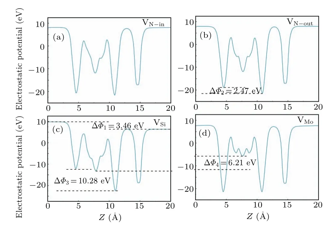
Fig.6.The effective electrostatic potentials of the MSN/Gr heterostructure with vacancies: (a)MSN/Gr VN-in,(b)MSN/Gr VN-out,(c)MSN/GrVSi and(d)MSN/GrVMo.
3.3.Modulation of the Schottky barrier height
The Schottky barrier height can commonly be effectively tuned by in-plane axial strain,external electric field and vertical strain engineering.The n-type and p-type Schottky barrier heights are defined as follows:
whereΦBnandΦBprepresent the barrier height for electrons and holes,respectively.ECBMandEVBMdenote the energy of the CBM and VBM of MSN.EFis the Fermi energy level,which is set to zero in this work.When the value ofΦBnis smaller than the value ofΦBp, an n-type Schottky contact is formed at the interface of the MSN/Gr heterostructure,and vice versa for a p-type Schottky contact.According to Fig.2(b),the calculatedΦBnandΦBpare 1.03 eV and 0.98 eV,respectively,and the sum ofΦBnandΦBpis equal to 2.01 eV.The value ofΦBnis larger thanΦBp,indicating a p-type Schottky is formed at the interface of the MSN/Gr heterostructure.
Since MSN/Gr heterostructure has a sizable Schottky barrier height, it is of great significance to achieve a low Schottky barrier height and contact resistance to enhance the device performance.Experimentally, one can achieve the modulation of the applied electric field by introducing pulsed ac fields or gate voltage.[43,44]The Gr and MoS2-based electrical devices have been successfully fabricated based on this technology.[45,46]Here,we define the positive direction of the applied external electric field pointing from the Gr layer to the MSN layer,which is consistent with the direction of the builtin electric field.Figure 7 shows the projected band structures of the MSN/Gr heterostructure under different external electric fields.Compared to the original MSN/Gr heterostructure without an external electric field,we find that the electric field only shifts the band structure up and down, while the trend of the band remains largely unchanged.It is noted that the Fermi energy level shifts towards the VBM of the MSN under the positive external electric field.Conversely,the Fermi energy level shifts towards the CBM of the MSN under the negative external electric field.The MSN in the MSN/Gr heterostructure retains the same characteristics as the direct bandgap semiconductor in the original heterostructure regardless of the positive or negative applied external electric field.
Furthermore, we plot the variation of the Schottky barrier heights under different external electric fields (Eext) of the MSN/Gr heterostructure in Fig.8.It is found that when the positive external electric field is applied, the value ofΦBngradually increases while the value ofΦBpgradually decreases.At the interface of the MSN/Gr heterostructure, the original p-type Schottky contact is maintained.When the negative external electric field is applied, the trends ofΦBnandΦBpare opposite to those of the positive applied electric field.As the negative electric field increases, the value ofΦBnbecomes smaller than the value ofΦBp,indicating that the n-type Schottky contact is formed at the interface of the MSN/Gr heterostructure.It is worth noting that the sum ofΦBnandΦBpis almost unchanged and the variation curve is almost a straight line.We also find that when the applied electric field is large to a certain extent(±0.5 V/°A),the Schottky barrier height becomes very small(close to zero).A vanishingly small Schottky barrier height and dynamic switching between n-type and p-type Schottky contacts are of great significance for achieving energy-efficient and high-performance Schottky barrier diodes and Schottky devices.
Contact resistance originating from the Schottky barrier greatly reduces the electrical performance of Schottky devices,so we design a tunable electrical diode based on MSN/Gr vertical contacts, as shown in Fig.9.The upward arrow indicates the positive direction of the applied electric field and the downward arrow indicates the negative direction of the applied electric field.Due to the ultra-high carrier mobility of the Gr,it can be used as an electrode to achieve efficient carrier injection.By changing the strength and direction of the external electric field, the electrical diode can be reconfigured to realize a small Schottky barrier height and dynamic switching between n-type and p-type Schottky contacts.The tunable electrical diode based on MSN/Gr vertical contacts may provide the possibility to exceed the capabilities of conventional Schottky diodes.

Fig.7.The projected band structures of the MSN/Gr heterostructure under different external electric fields(ranging from-0.5 V/°A to 0.5 V/°A).The Fermi level is set to zero and the yellow and green lines represent the contributions of the MSN and Gr,respectively.

Fig.8.The variation of the Schottky barrier heights under different external electric fields(Eext)of the MSN/Gr heterostructure.
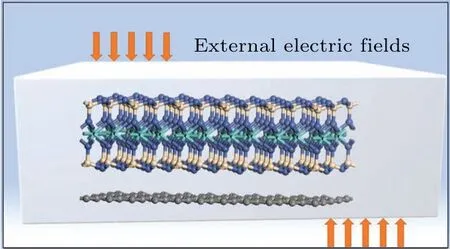
Fig.9.Schematic diagram of a tunable electrical diode based on MSN/Gr vertical contacts.
4.Conclusion
In summary, the effects of vacancy and external electric field on the electronic properties of the MSN/Gr heterostructure have been systematically investigated in this study based on first-principles calculation.Our results show the following:
(i)The band structure of the pristine MSN/Gr heterostructure is a simple superposition of the MSN band structure and the Gr band structure.We also find a charge transfer phenomenon at the interface between the Gr layer and the MSN layer,leading to the generation of a built-in electric field pointing from the Gr layer to the MSN layer.
(ii) For the pristine monolayer MSN,the introduction of N-in vacancy defect transforms the pristine MSN from a semiconductor to a half-metal.The introduction of N-out and Si vacancy defects transforms the pristine MSN from a semiconductor to a metal.While the introduction of Mo vacancy defect maintains the semiconductor nature of pristine MSN.For the pristine monolayer MSN and MSN/Gr heterostructure,the introduction of N-out and Mo vacancy defects cannot introduce magnetism into the original non-magnetic system.However,N-in and Si vacancy defects convert the original non-magnetic system into a magnetic system.
(iii) The work functions of the pristine monolayer MSN and MSN/Gr heterostructure decrease when N and Mo vacancies are introduced and increase when Si vacancy is introduced.In addition, the charge transfer at the interface of the MSN/Gr heterostructure decreases after the introduction of Nin and Si vacancy defects and increases after the introduction of N-out and Mo vacancy defects.N-out,Si and Mo vacancy defects raise the potentials at the positions of the corresponding defective atoms.
(iv)External electric field is an effective method to modulate the Schottky barrier height of the MSN/Gr heterostructure.Under the positive external electric field, the p-type Schottky contact is maintained.While under the positive external electric field,the MSN/Gr heterostructure can be modulated to realize the transition from the p-type contact to the n-type Schottky contact.Our results may provide a theoretical basis for the fabrication of energy-efficient and high-performance Schottky barrier diodes and Schottky devices.
Acknowledgements
Project supported by the Industry and Education Combination Innovation Platform of Intelligent Manufacturing and Graduate Joint Training Base at Guizhou University(Grant No.2020-520000-83-01-324061), the National Natural Science Foundation of China (Grant No.61264004), and the High-level Creative Talent Training Program in Guizhou Province of China(Grant No.[2015]4015).
杂志排行
Chinese Physics B的其它文章
- A multilayer network diffusion-based model for reviewer recommendation
- Speed limit effect during lane change in a two-lane lattice model under V2X environment
- Dynamics of information diffusion and disease transmission in time-varying multiplex networks with asymmetric activity levels
- Modeling the performance of perovskite solar cells with inserting porous insulating alumina nanoplates
- Logical stochastic resonance in a cross-bifurcation non-smooth system
- Experimental investigation of omnidirectional multiphysics bilayer invisibility cloak with anisotropic geometry
