Design of all-optical logic gate based on two-dimensional photonic crystal
2024-02-05WURongZHANGHaochenYANGJianye
WU Rong,ZHANG Hao-chen,YANG Jian-ye
(School of Electronic and Information Engineering, Lanzhou Jiaotong University, Lanzhou 730070, China)
Abstract: By embedding a line defect in a two-dimensional photonic crystal and using linear interference effect and waveguide coupling,an XNOR gate and NAND gate structure based on a two-dimensional photonic crystal is designed.The band structure of the two-dimensional photonic crystal is analyzed by using the plane wave expansion method.The time-domain finite-difference method and the linear interference effect are used to simulate the stable electric field diagram and the normalized power of the XNOR gate and NAND gates on the Rsoft platform.The simulation results demonstrate that the designed XNOR gate has a contrast of 29.5 dB,a response time of 0.073 ps,and a data transmission rate of 13.7 Tbit/s.On the other hand,the designed NAND gate has a contrast of up to 24.15 dB,a response time of 0.08 ps,and a data transmission rate of 12.5 Tbit/s.It can be seen that the designed structure has a high contrast,short response time,and fast data transmission rate.
Key words: photonic crystal;logic gate;finite difference time domain method;interference;contrast
1 Introduction
Photons have faster propagation speed and greater information-carrying capacity,making them increasingly favored over electricity as a form of light and with promising future applications.As a key component in optical information storage and processing,the all-optical switch has become a new device for optical communication and computing[1].Although photonic devices are gradually replacing electronic devices in many areas,electronic devices still dominate the market[2].One of the main reasons is the lack of practical all-optical switches and logic gates[3].Since all-optical logic gates can enable optical devices to achieve different output results under different input conditions,they can also achieve specific logic operation functions through the interaction between light waves[4].
Photonic crystals are synthetic artificial materials formed by periodic arrangement of media with different refractive indexes.According to the dimension,photonic crystals can be divided into onedimensional,two-dimensional,and three-dimensional photonic crystals.Compared to one-dimensional photonic crystals,two-dimensional photonic crystals have smaller limitations and a wider application range.Compared to three-dimensional photonic crystals,two-dimensional photonic crystals have a simpler structure,require a more skilled preparation process,exhibit a higher fault tolerance rate,and the finial product performance is better.Photonic crystals have two unique properties: photonic band gap and photonic localization.Photonic band gaps can make sure the light waves within a specific wavelength range transmit.Numerous optical devices with significant practical value have emerged due to the two characteristics of photonic crystals,including optical switches[5-6],optical wavelength division multiplexers[7],optical sensors[8-9],with the advantages of simple structures,low manufacturing complexity,and easy integration.
In the process of optical communication and optical computing,in order to solve the problem of low conversion efficiency and large loss of light and electricity,the all-optical network has become one of the research hotspots.All-optical logic gates,as the basis of the all-optical network,have received extensive attention from researchers[10].In 2017,Wu Ret al.[11]proposed 'NOR' and 'NOT' all-optical logic gates.The all-optical logic gate is mainly composed of four photonic crystal waveguides ports.Its compact size and quick response speed make it a highly efficient component.In 2019,Sun X Wet al.[12]used linear interference principle and selfcollimation effect to design all-optical logic gates such as 'XNOR','NOT',which possess simple structure,small size and high contrast.In 2022,Zhanget al.[13]through introducing defects in the perfect lattice and designed an all-optical half-adder structure composed of 'AND' and 'XOR'.The contrast of'CARRY' and 'SUM' reached 8.36 dB and 15.34 dB,respectively,and the response time was 3.63 ps.
On the basis of previous work,we mainly adopt waveguide coupling and linear interference effects to design all-optical structures for 'XNOR' and'NAND' operations based on two-dimensional photonic crystals.This expands the range of all-optical logic gates based on two-dimensional photonic crystals.The designed structure is simulated and analyzed using the Rsoft simulation platform,combined with the plane wave expansion method and the finite difference time domain method.It is found that the device size of the structure is small,the contrast is high,the response time is short,and the stability is good.
2 Theory
In this study,a photonic crystal with square lattice is used.The background material is air,and the circular dielectric column material is silicon.The refractive index of the dielectric column is 3.46,the lattice constant a is 0.506 μm,and the radius of the dielectric columnRis 0.2a.
To investigate the operational frequency range of the device,the plane wave expansion method is used to obtain the energy band diagram shown in Fig.1.The symbolsГ,XandMin the figure represent the coordinates of the reciprocal space in the Brillouin zone.It can be seen from Fig.1 that there are two photonic band gaps in photonic crystals only in the TE mode,and the high frequency region displays a narrow band gap.The normalized frequency is 1.336-1.378 0 (ωa/2πc),with a center frequency of 1.357 (ωa/2πc).The band gap in the low frequency region is narrow,the normalized frequency is 0.549-0.800 (ωa/2πc) and the center frequency is 0.674 5 (ωa/2πc).To enhance the output performance,a wavelength of 1.36-1.38 μm has been selected.

Fig.1 Energy band diagram of TE mode of photonic crystal

Fig.2 XOR gate structure
According to the waveguide theory,it is suggested that two optical signals transmitted in the same path experience phase-length and phase-cancellation interference[13].When the transmission phase difference between two beams of optical signals is 2mπ (m=0,1,2,···),the two optical signals are superimposed on each other,resulting in phaselength interference occurs between the optical signals.This enhances the signal strength at the output end,making it stronger than any individual beam of optical signals.When the phase difference between the two optical signals equals (2m+1) π,the two optical signals are partially cancelled,resulting in destructive interference occurs between the optical signals.Consequently,the signal strength at the output end is weaker than that of any other optical signal.
ContrastCRand response time are two crucial indicators to measure all-optical switches.ContrastCR=10lg(T1/T0)[14-15],whereT1represents the transmittance when the output port is logically '1',andT0represents the transmittance when the output port is logically '0'.The higher the contrast of the all-optical logic gate,the more sensitive and more stable its performance.The response time,also known as the adjustment time,is the duration required from the beginning of the output to stable output.Upon reaching the stable output,there will be a certain error,known as the error band,with a value of ±5% of the stable output value[16].
3 Design and simulation
3.1 NOR
All complex logic can be expressed in the form of simple and,or,not.This principle is fully reflected in the design process of all-optical logic gates..By transforming XOR logic using the inversion theorem,it is obtained that the NOR gate can be formed through cascading existing logic gates.According to NOR gate logic,when the two input ports are different the output port is '0',and when the two input ports are the same,the output port is'1'.The XOR function of the device can be considered as the XOR of the power,and this function is realized just through the expression (A+B)⊕1.The NOR gate structure,developed based on XOR gate,is shown in Figure 2.The structure is filled with 33×21 circular silicon dielectric columns in the air.Two input portsI1andI2represent a symmetrical structure,and Ref represents the reference signal.The reference signal Ref shares the same input structure as the input port,so both the reference signal and input signal have the same light wave intensity when they arrived at the output port.When the input signal is logic '00',(A+B)⊕1=1;when the input signal is logic '10' or '01',(A+B)⊕1=0;when the input signal is logic '11',and the input power isA+B=2,we can obtain an output of(A+B)⊕1=1.Figure 2 illustrates the optical path difference between the input signal and the reference signal to the output port OUT as 2a,causing input signalsI1andI2interfering with the reference signal Ref under different conditions.The light source signal is set to a continuous Gaussian light wave with a wavelength of 1.36 μm.The simulation results obtained by using the Rsoft simulation platform and the finite-difference time-domain method are shown in Fig.3-4.In this structure,when the input signal is either logical '01' or '10',the input signal and the reference signal destructively interfere in the output waveguide,and the intensity is the same so the output power is only 3×10⁻⁴Pin.Conversely,when the input signal is logical '00',only the reference signal Ref is output from the output waveguide,yielding an output power of 0.26Pin.When the input signal is logic '11',the two input signals will interfere with each other due to the same optical path difference to the output waveguide,and the intensity is half of the input power,thus,the output power is 0.27Pin.The contrast of the output port of the NOR gate stucture is as high as 29.5 dB,the response time is 0.073 ps,and the data transmission rate is 13.7 Tbit/s.
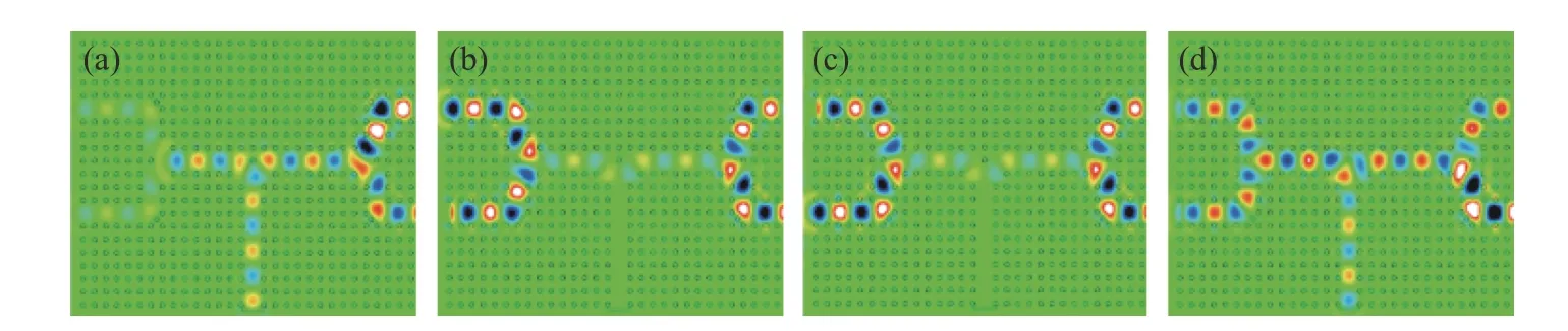
Fig.3 The steady-state electric field diagrams when the input is logic (a) '00',(b) '01',(c) '10' and (d) '11' respectively
It can be seen from Fig.4 that the output powerPoutchanges over time until it reaches 90% of the stable powerPavat timet1.Moreover,the Fig.4 indicates thatct1=88 μm,the transmission speed in photon air is 3×10⁸m/s,andt1=0.146 8 ps.When the output powerPoutreaches 10% of the stable powerPavfrom 0,it is denoted as timet11.Likewise,when the output powerPoutreaches 90% of the stable powerPavfrom 10% of the stable powerPav,it is denoted as timet12.Therefore,t1=t11+t12.According to Fig.4,t11=0.105 ps,andt12=0.041 8 ps.Likewise,when the output powerPoutreaches 90%of the stable powerPavfrom 10% of the stable powerPav,it is denoted as timet2.Due to the linear material used in this design,t2=2t12=0.083 6 ps.Therefore,the response period of the designed XOR gate isT=2t12+2t2=0.167 2 ps.
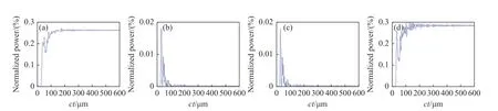
Fig.4 The normalized power output curves when the input is logic (a) '00',(b) '01',(c) '10' and (d) '11' respectively
3.2 NAND
Through the inversion theorem transformation and NOT-logical expression,can be obtained.The NAND gate structure shown in Fig.5 can be designed through the existing cascade of NOT gates and OR gates.The depicted structure comprises 29 × 21 circular silicon dielectric columns in the air.The light source signal is set to Gaussian continuous light wave with a wavelength of 1.38 μm.Since the designed AND gate uses only linear interference effect,no power requirement exists for the light source,thus the power of the light source defaults to 1.In Fig.5,the input signals areI1andI2,the reference signal is labeled Ref,and the output signal labeled OUT.The NOT logic of the input signalsI1,I2and the reference signal Ref can achieve by XOR.Since both the left and right parts of the structure have the same optical path difference,phase interference occurs in the output waveguide,functioning as an OR logic.As a result,the structure enables a cascade of NOT and OR logic.Fig.6 (color online) presents the simulation results.When both the input logic ofI1andI2are set to '00',constructive interference occurs when the two reference signals Ref are transmitted to the output waveguide,and the output power reaches 1.085Pin.Since the designed NAND gate has symmetrical structure,the output results for input logic '01' and '10' are same,only the input logic '10' is simulated.The input signalI1and the left reference signal Ref have destructive interference in the output waveguide.Moreover,the output power of the right reference signal Ref in the output waveguide is 0.26Pin.When the input logic is '11',the input signalsI1,I2,and the reference signal Ref undergo destructive interference at the output waveguide port.Consequently,the output power is only 0.001Pin.The output port of the NAND gate structure demonstrates a high contrast of 24.15 dB,a fast response time of 0.08 ps,and a data transmission rate of 12.5 Tbit/s.

Fig.5 NAND gate structure
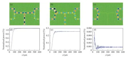
Fig.6 The stable electric field diagram and normalized power curve when the input logic is '00','10' and '11',respectively.(a)-(c) are electric field diagrams when input logic is (a) '00',(b) '10',and (c) '11';(d)-(f) are normalized curves when input logic is (d) '00',(e) '10',and (f) '00'
It can be seen from Fig.6 that the output powerPoutchanges over time.The time when the output powerPoutreaches 90% of the stable powerPavfrom 0 is denoted byt1.Further analysis of the figure represents thatct1=80 μm,andt1=0.267 ps can be calculated.The time when the output powerPoutreaches 10% of the stable powerPavfrom 0 is denoted ast11,and the time when the output powerPoutreaches 90% of the stable powerPavfrom 10% of the stable powerPavis denoted ast12.Therefore,t1=t11+t12.According to Fig.6,it can be seen thatt11=0.13 ps,andt12=0.137 ps.The time for the output powerPoutto reach 10% of the stable powerPavfrom 90% of the stable powerPavis denoted ast2.As the design uses linear materials,t2=2t12=0.274 ps.As a result,the response period of the designed NAND gate isT=2t12+2t2=0.548 ps.
Tab.1 Summarized features of proposed structure and previous works.
Tab.1 Summarized features of proposed structure and previous works
As can be seen from the table,the contrast of the output ports,both for the NOR gate and the NAND gate,have been improved considerably compared to the previous ones,which has a significant improvement in the performance of the logic device.
4 Conclusion
In a complete two-dimensional square lattice silicon photonic crystal,XOR gate and the NAND gate structures are designed by introducing line defects.The energy band structure of the photonic crystal was analyzed through plane wave expansion method.The Rsoft simulation platform was utilized to analyze the stable electric field and normalized power of the designed structure,employing the linear interference effect and the finite difference time domain method.The simulation results show that the designed same-or gate exhibits a high contrast of 29.5 dB,a response time of 0.073 ps,a response period of 0.167 2 ps,and a data transmission rate of 13.7 Tbit/s.In contrast,the designed NAND gate shows a contrast of up to 24.15 dB,a response time of 0.08 ps,a response period of 0.548 ps,and a data transmission rate of 12.5 Tbit/s.These parameters show that the designed structure exhibits high contrast,a short response time and a fast data transmission rate,with potential applications in the field of integrated optics.
杂志排行
中国光学的其它文章
- All-solid-state acousto-optic mode-locked laser operating at 660 nm
- Stimulated brillouin scattering in double-clad thulium-doped fiber amplifier
- Optical simulation design of surface mounted device beads for wide beam and high uniformity display
- 用于紫外光谱仪的探测器温度控制系统
- TDLAS 气体激光遥测高灵敏光电探测电路设计
- 空间目标轨道外热流计算及辐射特性研究